
In Praise of Digital Design: An Embedded
Systems Approach Using Verilog
“Peter Ashenden is leading the way towards a new curriculum for
educating the next generation of digital logic designers. Recognizing that
digital design has moved from being gate-centric assembly of custom
logic to processor-centric design of embedded systems, Dr. Ashenden has
shifted the focus from the gate to the modern design and integration of
complex integrated devices that may be physically realized in a variety of
forms. Dr. Ashenden does not ignore the fundamentals, but treats them
with suitable depth and breadth to provide a basis for the higher-level
material. As is the norm in all of Dr. Ashenden’s writing, the text is lucid
and a pleasure to read. The book is illustrated with copious examples and
the companion Web site offers all that one would expect in a text of such
high quality.”
—grant martin, Chief Scientist, Tensilica Inc.
“Dr. Ashenden has written a textbook that enables students to obtain a
much broader and more valuable understanding of modern digital system
design. Readers can be sure that the practices described in this book will
provide a strong foundation for modern digital system design using hard-
ware description languages.”
—gary spivey, George Fox University
“The convergence of miniaturized, sophisticated electronics into handheld,
low-power embedded systems such as cell phones, PDAs, and MP3 players
depends on efficient, digital design flows. Starting with an intuitive explo-
ration of the basic building blocks, Digital Design: An Embedded Systems
Approach introduces digital systems design in the context of embedded
systems to provide students with broader perspectives. Throughout the
text, Peter Ashenden’s practical approach engages students in understand-
ing the challenges and complexities involved in implementing embedded
systems.”
—gregory d. peterson, University of Tennessee
“Digital Design: An Embedded Systems Approach places emphasis on
larger systems containing processors, memory, and involving the design
and interface of I/O functions and application-specific accelerators. The
book’s presentation is based on a contemporary view that reflects the
real-world digital system design practice. At a time when the university
curriculum is generally lagging significantly behind industry development,
this book provides much needed information to students in the areas of
computer engineering, electrical engineering and computer science.”
—donald hung, San Jose State University
“Digital Design: An Embedded Systems Approach presents the design flow
of circuits and systems in a way that is both accessible and up-to-date.
Because the use of hardware description languages is state-of-the-art, it
is necessary that students learn how to use these languages along with
an appropriate methodology. This book presents a modern approach for
designing embedded systems starting with the fundamentals and progress-
ing up to a complete system—it is application driven and full of many
examples. I will recommend this book to my students.”
—goeran herrmann, TU Chemnitz
“Digital Design: An Embedded Systems Approach is surprisingly easy to
read despite the complexity of the material. It takes the reader in a journey
from the basics to a real understanding of digital design by answering the
‘whys’ and ‘hows’—it is persuasive and instructive as it moves deeper and
deeper into the material.”
—andrey koptyug, Mid Sweden University
“This up-to-date text on digital design is written in a very accessible style
using a modern design methodology and the real world of embedded
systems as its contexts. Digital Design: An Embedded Systems Approach
provides excellent coverage of all aspects of the design of embedded sys-
tems, with chapters not just on logic design itself, but also on processors,
memories, input/output interfacing and implementation technologies. It’s
particularly good at emphasizing the need to consider more than just logic
design when designing a digital system: the design has to be implemented
in the real world of engineering, where a whole variety of constraints,
such as circuit area, circuit interconnections, interfacing requirements,
power and performance, must be considered. For those who think logic
design is mundane, this book brings the subject to life.”
—roland ibbett,
University of Edinburgh
Digital Design
An Embedded Systems Approach
Using Verilog
about the author
Peter J. Ashenden is an Adjunct Associate Professor at Adelaide University
and the founder of Ashenden Designs, a consulting business specializing in
electronics design automation (EDA).
From 1990 to 2000, Dr. Ashenden was a member of the faculty
in the Department of Computer Science at Adelaide. He developed
curriculum and taught in a number of areas for both the Computer Sci-
ence and the Electrical and Electronic Engineering departments. Topics
included computer organization, computer architecture, digital logic
design, programming and algorithms, at all levels from undergraduate to
graduate courses. He was also actively involved in academic administra-
tion at many levels within the university.
In 2000, Dr. Ashenden established Ashenden Designs. His services
include training development and delivery, advising on design methodology,
research in EDA tool technology, development of design languages, and
standards writing. His clients include industry and government organiza-
tion in the United States, Europe and SE Asia.
Since 1992, Dr. Ashenden has been involved in the IEEE VHDL
standards committees, and continues to play a major role in ongoing
development of the language. From 2003 to 2005 he was Chair of the IEEE
Design Automation Standards Committee, which oversees development
of all IEEE standards in EDA. He is currently Technical Editor for the
VHDL, VHDL-AMS, and Rosetta specification language standards.
In addition to his research publications, Dr. Ashenden is author of
The Designer’s Guide to VHDL and The Student’s Guide to VHDL,
and coauthor of The System Designer’s Guide to VHSL-AMS and
VHDL-2007: Just the New Stuff. His VHDL books are highly regarded
and are the best-selling references on the subject. From 2000 to 2004,
he was Series Coeditor of the Morgan Kaufmann Series on Systems on
Silicon, and from 2001 to 2004 he was a member of the Editorial Board
of IEEE Design and Test of Computers magazine.
Dr. Ashenden is a Senior Member of the IEEE and the IEEE Computer
Society. He is also a volunteer Senior Firefighter of 12 years standing with
the South Australian Country Fire Service.

Digital Design
An Embedded Systems Approach
Using Verilog
peter j. ashenden
Adjunct Associate Professor
School of Computer Science
University of Adelaide
amsterdam • boston • heidelberg • london
new york • oxford • paris • san diego
san francisco • singapore • sydney • tokyo
Morgan Kaufmann is an imprint of Elsevier

Publishing Director Joanne Tracy
Publisher Denise E. M. Penrose
Acquisitions Editor Charles Glaser
Publishing Services Manager George Morrison
Senior Production Editor Dawnmarie Simpson
Developmental Editor Nate McFadden
Editorial Assistant Kimberlee Honjo
Production Assistant Lianne Hong
Cover Design Eric DeCicco
Cover Image Corbis
Composition diacriTech
Technical Illustration Peter Ashenden
Copyeditor JC Publishing
Proofreader Janet Cocker
Indexer Joan Green
Interior printer Sheridan Books, Inc.
Cover printer Phoenix Color, Inc.
Morgan Kaufmann Publishers is an imprint of Elsevier.
30 Corporate Drive, Suite 400, Burlington, MA 01803, USA
This book is printed on acid-free paper.
© 2008 by Elsevier Inc. All rights reserved.
Designations used by companies to distinguish their products are often claimed as trademarks or
registered trademarks. In all instances in which Morgan Kaufmann Publishers is aware of a claim,
the product names appear in initial capital or all capital letters. Readers, however, should contact the
appropriate companies for more complete information regarding trademarks and registration.
No part of this publication may be reproduced, stored in a retrieval system, or transmitted in any form
or by any means—electronic, mechanical, photocopying, scanning, or otherwise—without prior written
permission of the publisher.
Permissions may be sought directly from Elsevier’s Science & Technology Rights Department in Oxford,
UK: phone: (+44) 1865 843830, fax: (+44) 1865 853333, E-mail: permissions@elsevier.com. You may
also complete your request online via the Elsevier homepage (http://elsevier.com), by selecting “Support
& Contact” then “Copyright and Permission” and then “Obtaining Permissions.”
Library of Congress Cataloging-in-Publication Data
Ashenden, Peter J.
Digital design: an embedded systems approach using Verilog / Peter J. Ashenden.
p. cm.
Includes index.
ISBN 978-0-12-369527-7 (pbk. : alk. paper) 1. Embedded computer systems. 2. Verilog (Computer
hardware description language) 3. System design. I. Title.
TK7895.E42.A68 2007
621.39'16–dc22
2007023242
ISBN: 978-0-12-369527-7
For information on all Morgan Kaufmann publications,
visit our Web site at www.mkp.com or www.books.elsevier.com
Printed in the United States.
07 08 09 10 5 4 3 2 1
Working together to grow
libraries in developing countries
www.elsevier.com | www.bookaid.org | www.sabre.org
To my daughter, Eleanor
—pa
This page intentionally left blank
ix
contents
Preface . . . . . . . . . . . . . . . . . . . . . . . . . . . . . . . . . . . . . . . . . . . . . . . xv
chapter 1 Introduction and Methodology . . . . . . . . . . . 1
1.1 Digital Systems and Embedded Systems . . . . . . . . . . . . . . . . . 1
1.2 Binary Representation and Circuit Elements . . . . . . . . . . . . . 4
1.3 Real-World Circuits . . . . . . . . . . . . . . . . . . . . . . . . . . . . . . . . 9
1.3.1 Integrated Circuits . . . . . . . . . . . . . . . . . . . . . . . . . . 10
1.3.2 Logic Levels . . . . . . . . . . . . . . . . . . . . . . . . . . . . . . 11
1.3.3 Static Load Levels . . . . . . . . . . . . . . . . . . . . . . . . . . 13
1.3.4 Capacitive Load and Propagation Delay . . . . . . . . . 15
1.3.5 Wire Delay . . . . . . . . . . . . . . . . . . . . . . . . . . . . . . . 17
1.3.6 Sequential Timing . . . . . . . . . . . . . . . . . . . . . . . . . . 17
1.3.7 Power . . . . . . . . . . . . . . . . . . . . . . . . . . . . . . . . . . . 18
1.3.8 Area and Packaging . . . . . . . . . . . . . . . . . . . . . . . . . 19
1.4 Models . . . . . . . . . . . . . . . . . . . . . . . . . . . . . . . . . . . . . . . . . . 21
1.5 Design Methodology . . . . . . . . . . . . . . . . . . . . . . . . . . . . . . . 26
1.5.1 Embedded Systems Design . . . . . . . . . . . . . . . . . . . 31
1.6 Chapter Summary . . . . . . . . . . . . . . . . . . . . . . . . . . . . . . . . . 33
1.7 Further Reading . . . . . . . . . . . . . . . . . . . . . . . . . . . . . . . . . . . 34
Exercises . . . . . . . . . . . . . . . . . . . . . . . . . . . . . . . . . . . . . . . . 35
chapter 2 Combinational Basics . . . . . . . . . . . . . . . . . . 39
2.1 Boolean Functions and Boolean Algebra . . . . . . . . . . . . . . . . 39
2.1.1 Boolean Functions . . . . . . . . . . . . . . . . . . . . . . . . . . 39
2.1.2 Boolean Algebra . . . . . . . . . . . . . . . . . . . . . . . . . . . 48
2.1.3 Verilog Models of Boolean Equations . . . . . . . . . . . 51
2.2 Binary Coding . . . . . . . . . . . . . . . . . . . . . . . . . . . . . . . . . . . . 54
2.2.1 Using Vectors for Binary Codes . . . . . . . . . . . . . . . . 56
2.2.2 Bit Errors . . . . . . . . . . . . . . . . . . . . . . . . . . . . . . . . 58
2.3 Combinational Components and Circuits . . . . . . . . . . . . . . . 62
2.3.1 Decoders and Encoders . . . . . . . . . . . . . . . . . . . . . . 62
2.3.2 Multiplexers . . . . . . . . . . . . . . . . . . . . . . . . . . . . . . 68
2.3.3 Active-Low Logic . . . . . . . . . . . . . . . . . . . . . . . . . . 71
2.4 Verification of Combinational Circuits . . . . . . . . . . . . . . . . . . 74
2.5 Chapter Summary . . . . . . . . . . . . . . . . . . . . . . . . . . . . . . . . . 81
2.6 Further Reading . . . . . . . . . . . . . . . . . . . . . . . . . . . . . . . . . . . 82
Exercises . . . . . . . . . . . . . . . . . . . . . . . . . . . . . . . . . . . . . . . . 83
chapter 3 Numeric Basics . . . . . . . . . . . . . . . . . . . . . . . 87
3.1 Unsigned Integers . . . . . . . . . . . . . . . . . . . . . . . . . . . . . . . . . . 87
3.1.1 Coding Unsigned Integers . . . . . . . . . . . . . . . . . . . . 87
3.1.2 Operations on Unsigned Integers . . . . . . . . . . . . . . 92
3.1.3 Gray Codes . . . . . . . . . . . . . . . . . . . . . . . . . . . . . . . 116
3.2 Signed Integers . . . . . . . . . . . . . . . . . . . . . . . . . . . . . . . . . . . . 119
3.2.1 Coding Signed Integers . . . . . . . . . . . . . . . . . . . . . . 119
3.2.2 Operations on Signed Integers . . . . . . . . . . . . . . . . . 122
3.3 Fixed-Point Numbers . . . . . . . . . . . . . . . . . . . . . . . . . . . . . . . 131
3.3.1 Coding Fixed-Point Numbers . . . . . . . . . . . . . . . . . 131
3.3.2 Operations on Fixed-Point Numbers . . . . . . . . . . . . 136
3.4 Floating-Point Numbers . . . . . . . . . . . . . . . . . . . . . . . . . . . . . 138
3.4.1 Coding Floating-Point Numbers . . . . . . . . . . . . . . . 138
3.5 Chapter Summary . . . . . . . . . . . . . . . . . . . . . . . . . . . . . . . . . 143
3.6 Further Reading . . . . . . . . . . . . . . . . . . . . . . . . . . . . . . . . . . . 144
Exercises . . . . . . . . . . . . . . . . . . . . . . . . . . . . . . . . . . . . . . . . 144
chapter 4 Sequential Basics . . . . . . . . . . . . . . . . . . . . . . 151
4.1 Storage Elements . . . . . . . . . . . . . . . . . . . . . . . . . . . . . . . . . . 151
4.1.1 Flip-flops and Registers . . . . . . . . . . . . . . . . . . . . . . 151
4.1.2 Shift Registers . . . . . . . . . . . . . . . . . . . . . . . . . . . . . 161
4.1.3 Latches . . . . . . . . . . . . . . . . . . . . . . . . . . . . . . . . . . 162
4.2 Counters . . . . . . . . . . . . . . . . . . . . . . . . . . . . . . . . . . . . . . . . 167
4.3 Sequential Datapaths and Control . . . . . . . . . . . . . . . . . . . . . 175
4.3.1 Finite-State Machines . . . . . . . . . . . . . . . . . . . . . . . 179
4.4 Clocked Synchronous Timing Methodology . . . . . . . . . . . . . . 187
4.4.1 Asynchronous Inputs . . . . . . . . . . . . . . . . . . . . . . . . 192
4.4.2 Verification of Sequential Circuits . . . . . . . . . . . . . . 196
4.4.3 Asynchronous Timing Methodologies . . . . . . . . . . . 200
4.5 Chapter Summary . . . . . . . . . . . . . . . . . . . . . . . . . . . . . . . . . 203
4.6 Further Reading . . . . . . . . . . . . . . . . . . . . . . . . . . . . . . . . . . . 204
Exercises . . . . . . . . . . . . . . . . . . . . . . . . . . . . . . . . . . . . . . . . 205
chapter 5 Memories . . . . . . . . . . . . . . . . . . . . . . . . . . . 211
5.1 General Concepts . . . . . . . . . . . . . . . . . . . . . . . . . . . . . . . . . . 211
5.2 Memory Types . . . . . . . . . . . . . . . . . . . . . . . . . . . . . . . . . . . . 219
5.2.1 Asynchronous Static RAM . . . . . . . . . . . . . . . . . . . 220
5.2.2 Synchronous Static RAM . . . . . . . . . . . . . . . . . . . . . 222
x
CONTENTS
5.2.3 Multiport Memories . . . . . . . . . . . . . . . . . . . . . . . . 229
5.2.4 Dynamic RAM . . . . . . . . . . . . . . . . . . . . . . . . . . . . 233
5.2.5 Read-Only Memories . . . . . . . . . . . . . . . . . . . . . . . 235
5.3 Error Detection and Correction . . . . . . . . . . . . . . . . . . . . . . . 240
5.4 Chapter Summary . . . . . . . . . . . . . . . . . . . . . . . . . . . . . . . . . 244
5.5 Further Reading . . . . . . . . . . . . . . . . . . . . . . . . . . . . . . . . . . . 245
Exercises . . . . . . . . . . . . . . . . . . . . . . . . . . . . . . . . . . . . . . . . 246
chapter 6 Implementation Fabrics . . . . . . . . . . . . . . . . . 249
6.1 Integrated Circuits . . . . . . . . . . . . . . . . . . . . . . . . . . . . . . . . . 249
6.1.1 Integrated Circuit Manufacture . . . . . . . . . . . . . . . . 250
6.1.2 SSI and MSI Logic Families . . . . . . . . . . . . . . . . . . . 252
6.1.3 Application-Specific Integrated Circuits (ASICs) . . . 255
6.2 Programmable Logic Devices . . . . . . . . . . . . . . . . . . . . . . . . . 258
6.2.1 Programmable Array Logic . . . . . . . . . . . . . . . . . . . 258
6.2.2 Complex PLDs . . . . . . . . . . . . . . . . . . . . . . . . . . . . 262
6.2.3 Field-Programmable Gate Arrays . . . . . . . . . . . . . . 263
6.3 Packaging and Circuit Boards . . . . . . . . . . . . . . . . . . . . . . . . 269
6.4 Interconnection and Signal Integrity . . . . . . . . . . . . . . . . . . . . 272
6.4.1 Differential Signaling . . . . . . . . . . . . . . . . . . . . . . . . 276
6.5 Chapter Summary . . . . . . . . . . . . . . . . . . . . . . . . . . . . . . . . . 278
6.6 Further Reading . . . . . . . . . . . . . . . . . . . . . . . . . . . . . . . . . . . 279
Exercises . . . . . . . . . . . . . . . . . . . . . . . . . . . . . . . . . . . . . . . . 280
chapter 7 Processor Basics . . . . . . . . . . . . . . . . . . . . . . 281
7.1 Embedded Computer Organization . . . . . . . . . . . . . . . . . . . . 281
7.1.1 Microcontrollers and Processor Cores . . . . . . . . . . . 283
7.2 Instructions and Data . . . . . . . . . . . . . . . . . . . . . . . . . . . . . . . 285
7.2.1 The Gumnut Instruction Set . . . . . . . . . . . . . . . . . . 287
7.2.2 The Gumnut Assembler . . . . . . . . . . . . . . . . . . . . . . 296
7.2.3 Instruction Encoding . . . . . . . . . . . . . . . . . . . . . . . . 298
7.2.4 Other CPU Instruction Sets . . . . . . . . . . . . . . . . . . . 300
7.3 Interfacing with Memory . . . . . . . . . . . . . . . . . . . . . . . . . . . . 302
7.3.1 Cache Memory . . . . . . . . . . . . . . . . . . . . . . . . . . . . 307
7.4 Chapter Summary . . . . . . . . . . . . . . . . . . . . . . . . . . . . . . . . . 311
7.5 Further Reading . . . . . . . . . . . . . . . . . . . . . . . . . . . . . . . . . . . 311
Exercises . . . . . . . . . . . . . . . . . . . . . . . . . . . . . . . . . . . . . . . . 312
chapter 8 I/O Interfacing . . . . . . . . . . . . . . . . . . . . . . . 315
8.1 I/O Devices . . . . . . . . . . . . . . . . . . . . . . . . . . . . . . . . . . . . . . 315
8.1.1 Input Devices . . . . . . . . . . . . . . . . . . . . . . . . . . . . . 316
8.1.2 Output Devices . . . . . . . . . . . . . . . . . . . . . . . . . . . . 321
CONTENTS xi
8.2 I/O Controllers . . . . . . . . . . . . . . . . . . . . . . . . . . . . . . . . . . . . 330
8.2.1 Simple I/O Controllers . . . . . . . . . . . . . . . . . . . . . . 331
8.2.2 Autonomous I/O Controllers . . . . . . . . . . . . . . . . . 335
8.3 Parallel Buses . . . . . . . . . . . . . . . . . . . . . . . . . . . . . . . . . . . . . 338
8.3.1 Multiplexed Buses . . . . . . . . . . . . . . . . . . . . . . . . . . 338
8.3.2 Tristate Buses . . . . . . . . . . . . . . . . . . . . . . . . . . . . . 342
8.3.3 Open-Drain Buses . . . . . . . . . . . . . . . . . . . . . . . . . . 348
8.3.4 Bus Protocols . . . . . . . . . . . . . . . . . . . . . . . . . . . . . 349
8.4 Serial Transmission . . . . . . . . . . . . . . . . . . . . . . . . . . . . . . . . 353
8.4.1 Serial Transmission Techniques . . . . . . . . . . . . . . . . 353
8.4.2 Serial Interface Standards . . . . . . . . . . . . . . . . . . . . 357
8.5 I/O Software . . . . . . . . . . . . . . . . . . . . . . . . . . . . . . . . . . . . . 360
8.5.1 Polling . . . . . . . . . . . . . . . . . . . . . . . . . . . . . . . . . . . 360
8.5.2 Interrupts . . . . . . . . . . . . . . . . . . . . . . . . . . . . . . . . 362
8.5.3 Timers . . . . . . . . . . . . . . . . . . . . . . . . . . . . . . . . . . . 366
8.6 Chapter Summary . . . . . . . . . . . . . . . . . . . . . . . . . . . . . . . . . 373
8.7 Further Reading . . . . . . . . . . . . . . . . . . . . . . . . . . . . . . . . . . . 374
Exercises . . . . . . . . . . . . . . . . . . . . . . . . . . . . . . . . . . . . . . . . 375
chapter 9 Accelerators . . . . . . . . . . . . . . . . . . . . . . . . . 379
9.1 General Concepts . . . . . . . . . . . . . . . . . . . . . . . . . . . . . . . . . . 379
9.2 Case Study: Video Edge-Detection . . . . . . . . . . . . . . . . . . . . . 386
9.3 Verifying an Accelerator . . . . . . . . . . . . . . . . . . . . . . . . . . . . . 407
9.4 Chapter Summary . . . . . . . . . . . . . . . . . . . . . . . . . . . . . . . . . 419
9.5 Further Reading . . . . . . . . . . . . . . . . . . . . . . . . . . . . . . . . . . . 419
Exercises . . . . . . . . . . . . . . . . . . . . . . . . . . . . . . . . . . . . . . . . 420
chapter 10 Design Methodology . . . . . . . . . . . . . . . . . . 423
10.1 Design Flow . . . . . . . . . . . . . . . . . . . . . . . . . . . . . . . . . . . . . . 423
10.1.1 Architecture Exploration . . . . . . . . . . . . . . . . . . . . . 425
10.1.2 Functional Design . . . . . . . . . . . . . . . . . . . . . . . . . . 427
10.1.3 Functional Verification . . . . . . . . . . . . . . . . . . . . . . 429
10.1.4 Synthesis . . . . . . . . . . . . . . . . . . . . . . . . . . . . . . . . . 435
10.1.5 Physical Design . . . . . . . . . . . . . . . . . . . . . . . . . . . . 438
10.2 Design Optimization . . . . . . . . . . . . . . . . . . . . . . . . . . . . . . . 441
10.2.1 Area Optimization . . . . . . . . . . . . . . . . . . . . . . . . . 442
10.2.2 Timing Optimization . . . . . . . . . . . . . . . . . . . . . . . . 443
10.2.3 Power Optimization . . . . . . . . . . . . . . . . . . . . . . . . 448
10.3 Design for Test . . . . . . . . . . . . . . . . . . . . . . . . . . . . . . . . . . . . 451
10.3.1 Fault Models and Fault Simulation . . . . . . . . . . . . . 452
10.3.2 Scan Design and Boundary Scan . . . . . . . . . . . . . . . 454
10.3.3 Built-In Self Test (BIST) . . . . . . . . . . . . . . . . . . . . . 458
xii
CONTENTS
10.4 Nontechnical Issues . . . . . . . . . . . . . . . . . . . . . . . . . . . . . . . . 462
10.5 In Conclusion . . . . . . . . . . . . . . . . . . . . . . . . . . . . . . . . . . . . . 463
10.6 Chapter Summary . . . . . . . . . . . . . . . . . . . . . . . . . . . . . . . . . 465
10.7 Further Reading . . . . . . . . . . . . . . . . . . . . . . . . . . . . . . . . . . . 466
appendix a Knowledge Test Quiz Answers . . . . . . . . . . . 469
appendix b Introduction to Electronic Circuits . . . . . . . . 501
B.1 Components . . . . . . . . . . . . . . . . . . . . . . . . . . . . . . . . . . . . . . 501
B.1.1 Voltage Sources . . . . . . . . . . . . . . . . . . . . . . . . . . . . 502
B.1.2 Resistors . . . . . . . . . . . . . . . . . . . . . . . . . . . . . . . . . 502
B.1.3 Capacitors . . . . . . . . . . . . . . . . . . . . . . . . . . . . . . . . 503
B.1.4 Inductors . . . . . . . . . . . . . . . . . . . . . . . . . . . . . . . . . 503
B.1.5 MOSFETs . . . . . . . . . . . . . . . . . . . . . . . . . . . . . . . . 504
B.1.6 Diodes . . . . . . . . . . . . . . . . . . . . . . . . . . . . . . . . . . . 506
B.1.7 Bipolar Transistors . . . . . . . . . . . . . . . . . . . . . . . . . 507
B.2 Circuits . . . . . . . . . . . . . . . . . . . . . . . . . . . . . . . . . . . . . . . . . 508
B.2.1 Kirchhoff’s Laws . . . . . . . . . . . . . . . . . . . . . . . . . . . 508
B.2.2 Series and Parallel R, C, and L . . . . . . . . . . . . . . . . 509
B.2.3 RC Circuits . . . . . . . . . . . . . . . . . . . . . . . . . . . . . . . 511
B.2.4 RLC Circuits . . . . . . . . . . . . . . . . . . . . . . . . . . . . . . 512
B.3 Further Reading . . . . . . . . . . . . . . . . . . . . . . . . . . . . . . . . . . . 515
appendix c Verilog for Synthesis . . . . . . . . . . . . . . . . . . 517
C.1 Data Types and Operations . . . . . . . . . . . . . . . . . . . . . . . . . . 517
C.2 Combinational Functions . . . . . . . . . . . . . . . . . . . . . . . . . . . . 518
C.3 Sequential Circuits . . . . . . . . . . . . . . . . . . . . . . . . . . . . . . . . . 522
C.3.1 Finite-State Machines . . . . . . . . . . . . . . . . . . . . . . . 525
C.4 Memories . . . . . . . . . . . . . . . . . . . . . . . . . . . . . . . . . . . . . . . . 527
appendix d The Gumnut Microcontroller Core . . . . . . . . 531
D.1 The Gumnut Instruction Set . . . . . . . . . . . . . . . . . . . . . . . . . . 531
D.1.1 Arithmetic and Logical Instructions . . . . . . . . . . . . 531
D.1.2 Shift Instructions . . . . . . . . . . . . . . . . . . . . . . . . . . . 535
D.1.3 Memory and I/O Instructions . . . . . . . . . . . . . . . . . 536
D.1.4 Branch Instructions . . . . . . . . . . . . . . . . . . . . . . . . . 537
D.1.5 Jump Instructions . . . . . . . . . . . . . . . . . . . . . . . . . . 537
D.1.6 Miscellaneous Instructions . . . . . . . . . . . . . . . . . . . 538
D.2 The Gumnut Bus Interface . . . . . . . . . . . . . . . . . . . . . . . . . . . 538
Index . . . . . . . . . . . . . . . . . . . . . . . . . . . . . . . . . . . . . . . . . . . . . . . . 541
CONTENTS xiii
This page intentionally left blank
preface
APPROACH
This book provides a foundation in digital design for students in computer
engineering, electrical engineering and computer science courses. It deals
with digital design as an activity in a larger systems design context. Instead
of focusing on gate-level design and aspects of digital design that have
diminishing relevance in a real-world design context, the book concen-
trates on modern and evolving knowledge and design skills.
Most modern digital design practice involves design of embedded
systems, using small microcontrollers, larger CPUs/DSPs, or hard or soft
processor cores. Designs involve interfacing the processor or processors
to memory, I/O devices and communications interfaces, and developing
accelerators for operations that are too computationally intensive for pro-
cessors. Target technologies include ASICs, FPGAs, PLDs and PCBs. This
is a significant change from earlier design styles, which involved use of
small-scale integrated (SSI) and medium-scale integrated (MSI) circuits.
In such systems, the primary design goal was to minimize gate count or
IC package count. Since processors had lower performance and memories
had limited capacity, a greater proportion of system functionality was
implemented in hardware.
While design practices and the design context have evolved, many text-
books have not kept track. They continue to promote practices that are
largely obsolete or that have been subsumed into computer-aided design
(CAD) tools. They neglect many of the important considerations for mod-
ern designers. This book addresses the shortfall by taking an approach that
embodies modern design practice. The book presents the view that digital
logic is a basic abstraction over analog electronic circuits. Like any abstrac-
tion, the digital abstraction relies on assumptions being met and constraints
being satisfied. Thus, the book includes discussion of the electrical and tim-
ing properties of circuits, leading to an understanding of how they influence
design at higher levels of abstraction. Also, the book teaches a methodology
based on using abstraction to manage complexity, along with principles
and methods for making design trade-offs. These intellectual tools allow
students to track evolving design practice after they graduate.
Perhaps the most noticeable difference between this book and its
predecessors is the omission of material on Karnaugh maps and related
xv
logic optimization techniques. Some reviewers of the manuscript argued
that such techniques are still of value and are a necessary foundation for
students learning digital design. Certainly, it is important for students
to understand that a given function can be implemented by a variety of
equivalent circuits, and that different implementations may be more or
less optimal under different constraints. This book takes the approach of
presenting Boolean algebra as the foundation for gate-level circuit trans-
formation, but leaves the details of algorithms for optimization to CAD
tools. The complexity of modern systems makes it more important to
raise the level of abstraction at which we work and to introduce embed-
ded systems early in the curriculum. CAD tools perform a much better
job of gate-level optimization than we can do manually, using advanced
algorithms to satisfy relevant constraints. Techniques such as Karnaugh
maps do have a place, for example, in design of specialized hazard-free
logic circuits. Thus, students can defer learning about Karnaugh maps
until an advanced course in VLSI, or indeed, until they encounter the need
in industrial practice. A web search will reveal many sources describing
the techniques in detail, including an excellent article in Wikipedia.
The approach taken in this book makes it relevant to Computer Sci-
ence courses, as well as to Computer Engineering and Electrical Engi-
neering courses. By treating digital design as part of embedded systems
design, the book will provide the understanding of hardware needed for
computer science students to analyze and design systems comprising
both hardware and software components. The principles of abstraction
and complexity management using abstraction presented in the book are
the same as those underlying much of computer science and software
engineering.
Modern digital design practice relies heavily on models expressed in
hardware description languages (HDLs), such as Verilog and VHDL. HDL
models are used for design entry at the abstract behavioral level and for
refinements at the register transfer level. Synthesis tools produce gate-level
HDL models for low-level verification. Designers also express verification
environments in HDLs. This book emphasizes HDL-based design and
verification at all levels of abstraction. The present version uses Verilog
for this purpose. A second version, Digital Design: An Embedded Systems
Approach Using VHDL, substitutes VHDL for the same purpose.
OVERVIEW
For those who are musically inclined, the organization of this book can be
likened to a two-act opera, complete with overture, intermezzo, and finale.
Chapter 1 forms the overture, introducing the themes that are to fol-
low in the rest of the work. It starts with a discussion of the basic ideas of
the digital abstraction, and introduces the basic digital circuit elements.
xvi PREFACE
It then shows how various non-ideal behaviors of the elements impose
constraints on what we can design. The chapter finishes with a discussion
of a systematic process of design, based on models expressed in a hard-
ware description language.
Act I of the opera comprises Chapters 2 through 5. In this act, we
develop the themes of basic digital design in more detail.
Chapter 2 focuses on combinational circuits, starting with Boolean
algebra as the theoretical underpinning and moving on to binary coding
of information. The chapter then surveys a range of components that can
be used as building blocks in larger combinational circuits, before return-
ing to the design methodology to discuss verification of combinational
circuits.
Chapter 3 expands in some detail on combinational circuits used
to process numeric information. It examines various binary codes for
unsigned integers, signed integers, fixed-point fractions and floating-point
real numbers. For each kind of code, the chapter describes how some
arithmetic operations can be performed and looks at combinational cir-
cuits that implement arithmetic operations.
Chapter 4 introduces a central theme of digital design, sequential cir-
cuits. The chapter examines several sequential circuit elements for storing
information and for counting events. It then describes the concepts of a
datapath and a control section, followed by a description of the clocked
synchronous timing methodology.
Chapter 5 completes Act I, describing the use of memories for storing
information. It starts by introducing the general concepts that are com-
mon to all kinds of semiconductor memory, and then focuses on the par-
ticular features of each type, including SRAM, DRAM, ROM and flash
memories. The chapter finishes with a discussion of techniques for dealing
with errors in the stored data.
The intermezzo, Chapter 6, is a digression away from functional
design into physical design and the implementation fabrics used for digi-
tal systems. The chapter describes the range of integrated circuits that are
used for digital systems, including ASICSs, FPGAs and other PLDs. The
chapter also discusses some of the physical and electrical characteristics of
implementation fabrics that give rise to constraints on designs.
Act II of the opera, comprising Chapters 7 through 9, develops the
embedded systems theme.
Chapter 7 introduces the kinds of processors that are used in embed-
ded systems and gives examples of the instructions that make up embed-
ded software programs. The chapter also describes the way instructions
and data are encoded in binary and stored in memory and examines ways
of connecting the processor with memory components.
Chapter 8 expands on the notion of input/output (I/O) controllers
that connect an embedded computer system with devices that sense and
PREFACE xvii
affect real-world physical properties. It describes a range of devices that
are used in embedded computers and shows how they are accessed by an
embedded processor and by embedded software.
Chapter 9 describes accelerators, that is, components that can be
added to embedded systems to perform operations faster than is possible
with embedded software running on a processor core. This chapter uses
an extended example to illustrate design considerations for accelerators,
and shows how an accelerator interacts with an embedded processor.
The finale, Chapter 10, is a coda that returns to the theme of design
methodology introduced in Chapter 1. The chapter describes details of
the design flow and discusses how aspects of the design can be optimized
to better meet constraints. It also introduces the concept of design for
test, and outlines some design for test tools and techniques. The opera
finishes with a discussion of the larger context in which digital systems
are designed.
After a performance of an opera, there is always a lively discussion
in the foyer. This book contains a number of appendices that correspond
to that aspect of the opera. Appendix A provides sample answers for the
Knowledge Test Quiz sections in the main chapters. Appendix B provides
a quick refresher on electronic circuits. Appendix C is a summary of the
subset of Verilog used for synthesis of digital circuits. Finally, Appendix D
is an instruction-set reference for the Gumnut embedded processor core
used in examples in Chapters 7 through 9.
For those not inclined toward classical music, I apologize if the pre-
ceding is not a helpful analogy. An analogy with the courses of a feast
came to mind, but potential confusion among readers in different parts
of the world over the terms appetizer, entrée and main course make the
analogy problematic. The gastronomically inclined reader should feel free
to find the correspondence in accordance with local custom.
COURSE ORGANIZATION
This book covers the topics included in the Digital Logic knowledge area of
the Computer Engineering Body of Knowledge described in the IEEE/ACM
Curriculum Guidelines for Undergraduate Degree Programs in Computer
Engineering. The book is appropriate for a course at the sophomore level,
assuming only previous introductory courses in electronic circuits and com-
puter programming. It articulates into junior and senior courses in embed-
ded systems, computer organization, VLSI and other advanced topics.
For a full sequence in digital design, the chapters of the book can be
covered in order. Alternatively, a shorter sequence could draw on Chapter 1
through Chapter 6 plus Chapter 10. Such a sequence would defer material
in Chapters 7 through 9 to a subsequent course on embedded systems
design.
xviii
PREFACE
For either sequence, the material in this book should be supplemented
by a reference book on the Verilog language. The course work should
also include laboratory projects, since hands-on design is the best way to
reinforce the principles presented in the book.
WEB SUPPLEMENTS
No textbook can be complete nowadays without supplementary material
on a website. For this book, resources for students and instructors are
available at the website:
textbooks.elsevier.com/9780123695277
For students, the website contains:
Source code for all of the example HDL models in the book
Tutorials on the VHDL and Verilog hardware description languages
An assembler for the Gumnut processor described in Chapter 7 and
Appendix D
A link to the ISE WebPack FPGA EDA tool suite from Xilinx
A link to the ModelSim Xilinx Edition III VHDL and Verilog simula-
tor from Mentor Graphics Corporation
A link to an evaluation edition of the Synplify Pro PFGA synthesis
tool from Synplicity, Inc. (see inside back cover for more details).
Tutorials on use of the EDA tools for design projects
For instructors, the website contains a protected area with additional
resources:
An instructor’s manual
Suggested lab projects
Lecture notes
Figures from the text in JPG and PPT formats
Instructors are invited to contribute additional material for the benefit of
their colleagues.
Despite the best efforts of all involved, some errors have no doubt
crept through the review and editorial process. A list of detected errors
will be available accumulated on the website mentioned above. Should
you detect such an error, please check whether it has been previously
recorded. If not, I would be grateful for notice by email to
왘
왘
왘
왘
왘
왘
왘
왘
왘
왘
왘
PREFACE xix
I would also be delighted to hear feedback about the book and supplementary
material, including suggestions for improvement.
ACKNOWLEDGMENTS
This book arose from my long-standing desire to bring a more modern
approach to the teaching of digital design. I am deeply grateful to the
folks at Morgan Kaufmann Publishers for supporting me in realizing this
goal, and for their guidance and advice in shaping the book. Particular
thanks go to Denise Penrose, Publisher; Nate McFadden, Developmental
Editor and Kim Honjo, Editorial Assistant. Thanks also to Dawnmarie
Simpson at Elsevier for meticulous attention to detail and for making the
production process go like clockwork.
The manuscript benefited from comprehensive reviews by Dr. A. Bou-
ridane, Queen’s University Belfast; Prof. Goeran Herrmann, Chemnitz
University of Technology; Prof. Donald Hung, San Jose State Univer-
sity; Prof. Roland Ibbett, University of Edinburgh; Dr. Andrey Koptyug,
Mid Sweden University; Dr. Grant Martin, Tensilica, Inc.; Dr. Gregory
D. Peterson, University of Tennessee; Brian R. Prasky, IBM; Dr. Gary
Spivey, George Fox University; Dr. Peixin Zhong, Michigan State Univer-
sity; and an anonymous reviewer from Rensselaer Polytechnic Institute.
Also, my esteemed colleague Cliff Cummings of Sunburst Design, Inc.,
provided technical reviews of the Verilog code and related text. To all of
these, my sincere thanks for their contributions. The immense improve-
ment from my first draft to the final draft is due to their efforts.
The book and the associated teaching materials also benefited from
field testing: in alpha form by myself at the University of Adelaide and
by Dr. Monte Tull at The University of Oklahoma; and in beta form by
James Sterbenz at The University of Kansas. To them and to their stu-
dents, thanks for your forbearance with the errors and for your valuable
feedback.
xx
PREFACE
1
1
introduction and
methodology
This first chapter introduces some of the fundamental ideas underlying
design of modern digital systems. We cover quite a lot of ground, but at
a fairly basic level. The idea is to set the context for more detailed discus-
sion in subsequent chapters.
We start by looking at the basic circuit elements from which digital
systems are built, and seeing some of the ways in which they can be put
together to perform a required function. We also consider some of the
nonideal effects that we need to keep in mind, since they impose con-
straints on what we can design. We then focus on a systematic process of
design, based on models expressed in a hardware description language.
Approaching the design process systematically allows us to develop com-
plex systems that meet modern application requirements.
1.1 DIGITAL SYSTEMS AND
EMBEDDED SYSTEMS
This book is about digital design. Let’s take a moment to explore those
two words. Digital refers to electronic circuits that represent informa-
tion in a special way, using just two voltage levels. The main rationale
for doing this is to increase the reliability and accuracy of the circuits,
but as we will see, there are numerous other benefits that flow from the
digital approach. We also use the term logic to refer to digital circuits. We
can think of the two voltage levels as representing truth values, leading
us to use rules of logic to analyze digital circuits. This gives us a strong
mathematical foundation on which to build. The word design refers to
the systematic process of working out how to construct circuits that meet
given requirements while satisfying constraints on cost, performance,
power consumption, size, weight and other properties. In this book,
we focus on the design aspects and build a methodology for designing
complex digital systems.
2 CHAPTER ONE introduction and methodology
Digital circuits have quite a long and interesting history. They were
preceded by mechanical systems, electromechanical systems, and analog
electronic systems. Most of these systems were used for numeric com-
putations in business and military applications, for example, in ledger
calculations and in computing ballistics tables. However, they suffered
from numerous disadvantages, including inaccuracy, low speed, and high
maintenance.
Early digital circuits, built in the mid-twentieth century, were con-
structed with relays. The contacts of a relay are either open, blocking
current flow, or closed, allowing current to flow. Current controlled in
this manner by one or more relays could then be used to switch other
relays. However, even though relay-based systems were more reliable than
their predecessors, they still suffered from reliability and performance
problems.
The advent of digital circuits based on vacuum tubes and, sub-
sequently, transistors led to major improvements in reliability and
performance. However, it was the invention of the integrated circuit (IC),
in which multiple transistors were fabricated and connected together,
that really enabled the “digital revolution.” As manufacturing technol-
ogy has developed, the size of transistors and the interconnecting wires
has shrunk. This, along with other factors, has led to ICs, containing
billions of transistors and performing complex functions, becoming
commonplace now.
At this point, you may be wondering how such complex circuits can
be designed. In your electronic circuits course, you may have learned how
transistors operate, and that their operation is determined by numerous
parameters. Given the complexity of designing a small circuit containing
a few transistors, how could it be possible to design a large system with
billions of transistors?
The key is abstraction. By abstraction, we mean identifying aspects
that are important to a task at hand, and hiding details of other aspects.
Of course, the other aspects can’t be ignored arbitrarily. Rather, we make
assumptions and follow disciplines that allow us to ignore those details
while we focus on the aspects of interest. As an example, the digital
abstraction involves only allowing two voltage levels in a circuit, with
transistors being either turned “on” (that is, fully conducting) or turned
“off” (that is, not conducting). One of the assumptions we make in sup-
porting this abstraction is that transistors switch on and off virtually
instantaneously. One of the design disciplines we follow is to regulate
switching to occur within well-defined intervals of time, called “clock
periods.” We will see many other assumptions and disciplines as we pro-
ceed. The benefit of the digital abstraction is that it allows us to apply
much simpler analysis and design procedures, and thus to build much
more complex systems.
1.1 Digital Systems and Embedded Systems CHAPTER ONE 3
The circuits that we will deal with in this book all perform functions
that involve manipulating information of various kinds over time. The
information might be an audio signal, the position of part of a machine,
or the temperature of a substance. The information may change over time,
and the way in which it is manipulated may vary with time.
Digital systems are electronic circuits that represent information in
discrete form. An example of the kind of information that we might rep-
resent is an audio sound. In the real world, a sound is a continuously vary-
ing pressure waveform, which we might represent mathematically using
a continuous function of time. However, representing that function with
any significant precision as a continuously varying electrical signal in a
circuit is difficult and costly, due to electrical noise and variation in circuit
parameters. A digital system, on the other hand, represents the signal as
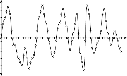
a stream of discrete values sampled at discrete points in time, as shown
in Figure 1.1. Each sample represents an approximation to the pressure
value at a given instant. The approximations are drawn from a discrete
set of values, for example, the set {10.0, 9.9, 9.8, . . . , 0.1, 0.0,
0.1, . . . , 9.9, 10.0}. By limiting the set of values that can be represented,
we can encode each value with a unique combination of digital values,
each of which is either a low or high voltage. We shall see exactly how
we might do that in Chapter 2. Furthermore, by sampling the signal at
regular intervals, say, every 50s, the rate and times at which samples
arrive and must be processed is predictable.
Discrete representations of information and discrete sequencing in
time are fundamental abstractions. Much of this book is about how to
choose appropriate representations, how to process information thus rep-
resented, how to sequence the processing, and how to ensure that the
assumptions supporting the abstractions are maintained.
The majority of digital systems designed and manufactured today are
embedded systems, in which much of the processing work is done by one
FIGURE 1.1 A pressure
waveform of a sound, continuously
varying over time, and the discrete
representation of the waveform in
a digital system.
4 CHAPTER ONE introduction and methodology
or more computers that form part of the system. In fact, the vast majority
of computers in use today are in embedded systems, rather than in PCs
and other general purpose systems. Early computers were large systems
in their own right, and were rarely considered as components of larger
systems. However, as technology developed, particularly to the stage of
IC technology, it became practical to embed small computers as compo-
nents of a circuit and to program them to implement part of the circuit’s
functionality. Embedded computers usually do not take the same form as
general purpose computers, such as desktop or portable PCs. Instead, an
embedded computer consists of a processor core, together with memory
components for storing the program and data for the program to run on
the processor core, and other components for transferring data between
the processor core and the rest of the system.
The programs running on processor cores form the embedded soft-
ware of a system. The way in which embedded software is written bears
both similarities and differences with software development for general
purpose computers. It is a large topic area in its own right and is beyond
the scope of this book. Nonetheless, since we are dealing with embedded
systems in this book, we need to address embedded software at least at a
basic level. We will return to the topic as part of our discussion of interfac-
ing with embedded processor cores in Chapters 8 and 9.
Since most digital systems in use today are embedded systems, most
digital design practice involves developing the interface circuitry around
processor cores and the application-specific circuitry to perform tasks not
done by the cores. That is why this book deals specifically with digital
design in the context of embedded systems.
1.2 BINARY REPRESENTATION AND
CIRCUIT ELEMENTS
The simplest discrete representation that we see in a digital system is called
a binary representation. It is a representation of information that can have
only two values. Examples of such information include:
whether a switch is open or closed
whether a light is on or off
whether a microphone is active or muted
We can think of these as logical conditions: each is either true or
false. In order to represent them in a digital circuit, we can assign a
high voltage level to represent the value true, and a low voltage level to
represent the value false. (This is just a convention, called positive logic,
or active-high logic. We could make the reverse assignment, leading to
negative logic, or active-low logic, which we will discuss in Chapter 2.)
We often use the values 0 and 1 instead of false and true, respectively.
왘
왘
왘
The values 0 and 1 are binary (base 2) digits, or bits, hence the term
binary representation.
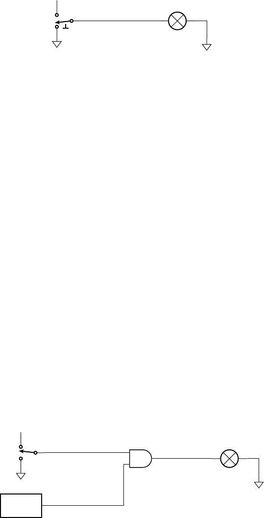
The circuit shown in Figure 1.2 illustrates the idea of binary
representation. The signal labeled switch_pressed represents the state of
the switch. When the push-button switch is pressed, the signal has a high
voltage, representing the truth of the condition, “the switch is pressed.”
When the switch is not pressed, the signal has a low voltage, representing
the falsehood of the condition. Since illumination of the lamp is controlled
by the switch, we could equally well have labeled the signal lamp_lit, with
a high voltage representing the truth of the condition, “the lamp is lit,”
and a low voltage representing the falsehood of the condition.
A more complex digital circuit is shown in Figure 1.3. This circuit
includes a light sensor with a digital output, dark, that is true (high volt-
age) when there is no ambient light, or false (low voltage) otherwise. The
circuit also includes a switch that determines whether the digital signal
lamp_enabled is low or high (that is, false or true, respectively). The sym-
bol in the middle of the figure represents an AND gate, a digital circuit
element whose output is only true (1) if both of its inputs are true (1).
The output is false (0) if either input is false (0). Thus, in the circuit, the
signal lamp_lit is true if lamp_enabled is true and dark is true, and is false
otherwise. Given this behavior, we can apply laws of logic to analyze
the circuit. For example, we can determine that if there is ambient light,
the lamp will not light, since the logical AND of two conditions yields
falsehood when either of the conditions is false.
The AND gate shown in Figure 1.3 is just one of several basic digital
logic components. Some others are shown in Figure 1.4. The AND gate, as
FIGURE 1.3 A digital circuit
for a night-light that is only lit
when the switch is on and the light
sensor shows that it is dark.
lamp_enabled
dark
lamp_lit
sensor
+V
1.2 Binary Representation and Circuit Elements CHAPTER ONE 5
switch_pressed
+V
FIGURE 1.2 A circuit in
which a switch controls a lamp.
6 CHAPTER ONE introduction and methodology
we mentioned above, produces a 1 on its output if both inputs are 1, or a 0
on the output if either input is 0. The OR gate produces the “inclusive or” of
its inputs. Its output is 1 if either or both of the inputs is 1, or 0 if both inputs
are 0. The inverter produces the “negation” of its input. Its output is 1 if the
input is 0, or 0 if the input is 1. Finally, the multiplexer selects between the
two inputs labeled “0” and “1” based on the value of the “select” input at
the bottom of the symbol. If the select input has the value 0, then the output
has the same value as that on the “0” input, whereas if the select input has
the value 1, then the output has the same value as that on the “1” input.
We can use these logic gates to build digital circuits that implement
more complex logic functions.
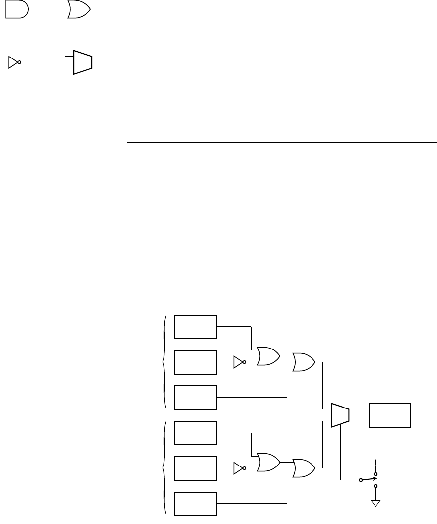
example 1.1 Suppose a factory has two vats, only one of which is used at
a time. The liquid in the vat in use needs to be at the right temperature, between
25˚C and 30˚C. Each vat has two temperature sensors indicating whether the
temperature is above 25˚C and above 30˚C, respectively. The vats also have low-
level sensors. The supervisor needs to be woken up by a buzzer when the temper-
ature is too high or too low or the vat level is too low. He has a switch to select
which vat is in use. Design a circuit of gates to activate the buzzer as required.
solution For the selected vat, the condition for activating the buzzer is
“temperature not above 25˚C or temperature above 30˚C, or level low.” This
can be implemented with a gate circuit for each vat. The switch can be used to
control the select input of a multiplexer to choose between the circuit outputs
for the two vats. The output of the multiplexer then activates the buzzer. The
complete circuit is shown in Figure 1.5.
AND gate OR gate
inverter multiplexer
0
1
FIGURE 1.4 Basic digital
logic gates.
>30°C
low level
buzzer
>25°C
>30°C
low level
>25°C
0
1
vat 0
vat 1 select vat 1
select vat 0
+V
FIGURE1.5 The vat buzzer
circuit.
1.2 Binary Representation and Circuit Elements CHAPTER ONE 7
Circuits such as those considered above are called combinational.
This means that the values of the circuit’s outputs at any given time are
determined purely by combining the values of the inputs at that time.
There is no notion of storage of information, that is, dependence on val-
ues at previous times. While combinational circuits are important as parts
of larger digital systems, nearly all digital systems are sequential. This
means that they do include some form of storage, allowing the values of
outputs to be determined by both the current input values and previous
input values.
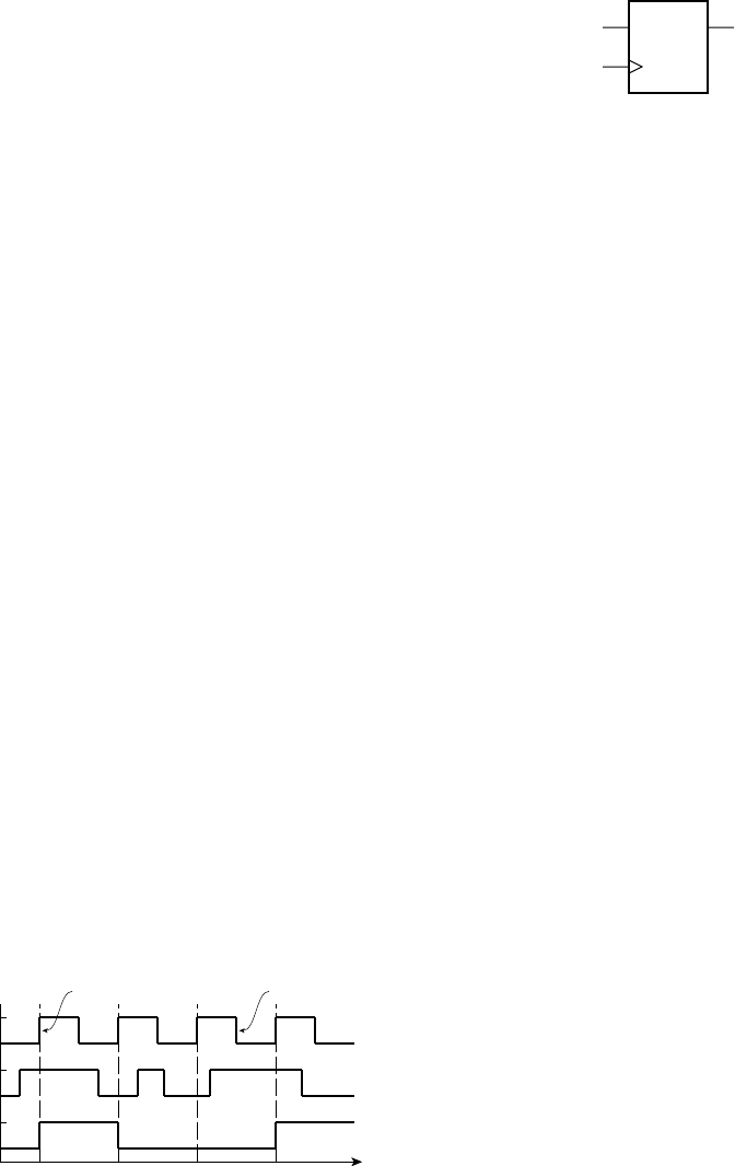
One of the simplest digital circuit elements for storing information is
called, somewhat prosaically, a flip-flop. It can “remember” a single bit
of information, allowing it to “flip” and “flop” between a stored 0 state
and a stored 1 state. The symbol for a D flip-flop is shown in Figure 1.6.
It is called a “D” flip-flop because it has a single input,
D, representing
the value of the data to be stored: “D” for “data.” It also has another
input, clk, called the clock input, that indicates when the value of the
D input should be stored. The behavior of the D flip-flop is illustrated
in the timing diagram in Figure 1.7. A timing diagram is a graph of the
values of one or more signals as they change with time. Time extends
along the horizontal axis, and the signals of interest are listed on the
vertical axis. Figure 1.7 shows the D input of the flip-flop changing at
irregular intervals and the clk input changing periodically. A transition
of clk from 0 to 1 is called a rising edge of the signal. (Similarly, a transi-
tion from 1 to 0 is called a falling edge.) The small triangular marking
next to the clk input specifies that the D value is stored only on a rising
edge of the clk input. At that time, the Q output changes to reflect the
stored value. Any subsequent changes on the D input are ignored until
the next rising edge of clk. A circuit element that behaves in this way is
called edge-triggered.
While the behavior of a flip-flop does not depend on the clock input
being periodic, in nearly all digital systems, there is a single clock signal
that synchronizes all of the storage elements in the system. The system
is composed of combinational circuits that perform logical functions on
the values of signals and flip-flops that store intermediate results. As we
DQ
clk
FIGURE 1.6 A D fl ip-fl op.
FIGURE 1.7 Timing diagram
for a D fl ip-fl op.
D
0
1
clk
0
1
Q
0
1
rising edge falling edge
8 CHAPTER ONE introduction and methodology
shall see, use of a single periodic synchronizing clock greatly simplifies
design of the system. The clock operates at a fixed frequency and divides
time into discrete intervals, called clock periods, or clock cycles. Modern
digital circuits operate with clock frequencies in the range of tens to
hundreds of megahertz (MHz, or millions of cycles per second), with
high-performance circuits extending up to several gigahertz (GHz, or
billions of cycles per second). Division of time into discrete intervals allows
us to deal with time in a more abstract form. This is another example of
abstraction at work.
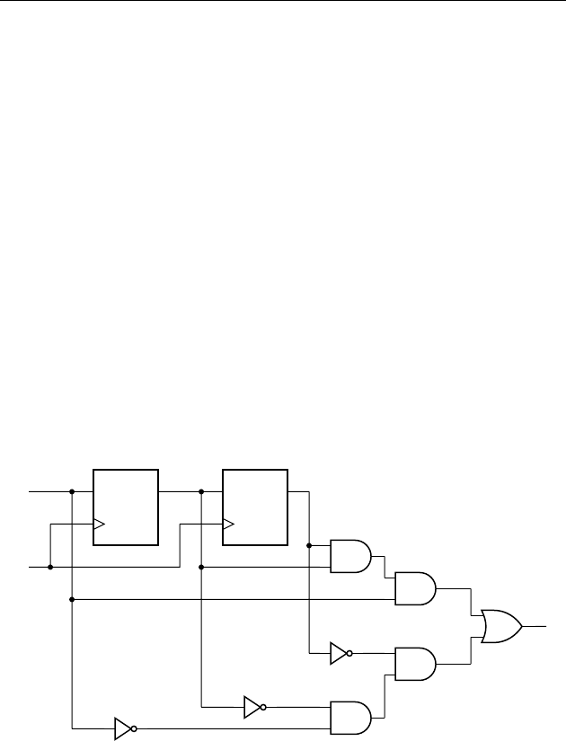
example 1.2 Develop a sequential circuit that has a single data input sig-
nal,
S, and produces an output Y. The output is 1 whenever S has the same value
over three successive clock cycles, and 0 otherwise. Assume that the value of
S
for a given clock cycle is defi ned at the time of the rising clock edge at the end of
the clock cycle.
solution In order to compare the values of S in three successive clock
cycles, we need to save the values of
S for the previous two cycles and compare
them with the current value of
S. We can use a pair of D fl ip-fl ops, connected in
a pipeline as shown in Figure 1.8, to store the values. When a clock edge occurs,
the fi rst fl ip-fl op,
ff 1, stores the value of S from the preceding clock cycle. That
value is passed onto the second fl ip-fl op,
ff 2, so that at the next clock edge, ff 2
stores the value of
S from two cycles prior.
The output Y is 1 if and only if three successive value of S are all 1 or are all 0.
Gates
g1 and g2 jointly determine if the three values are all 1. Inverters g3, g4
and
g5 negate the three values, and so gates g6 and g7 determine if the three
values are all 0. Gate
g8 combines the two alternatives to yield the final
output.
DQ
clk
DQ
clk
Y
S
clk
ff1
S1
S2
Y1
Y0
ff2
g1
g2
g6
g7
g8
g3
g4
g5
FIGURE 1.8 A sequential
circuit for comparing successive
bits of an input.
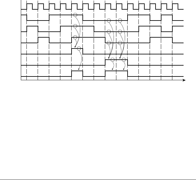
Figure 1.9 shows a timing diagram of the circuit for a particular sequence of
input values on
S over several clock cycles. The outputs of the two fl ip-fl ops
follow the value of
S, but are delayed by one and two clock cycles, respectively.
This timing diagram shows the value of
S changing at the time of a clock edge.
The fl ip-fl op will actually store the value that is on
S immediately before the
clock edge. The circles and arrows indicate which signals are used to determine
the values of other signals, leading to a 1 at the output. When all of
S, S1 and S2
are 1,
Y1 changes to 1, indicating that S has been 1 for three successive cycles.
Similarly, when all of
S, S1 and S2 are 0, Y0 changes to 1, indicating that
S has been 0 for three successive cycles. When either of Y1 or Y0 is 1, the output
Y changes to 1.
1. What are the two values used in binary representation?
2. If one input of an AND gate is 0 and the other is 1, what is the
output value? What if both are 0, or both are 1?
3. If one input of an OR gate is 0 and the other is 1, what is the output
value? What if both are 0, or both are 1?
4. What function is performed by a multiplexer?
5. What is the distinction between combinational and sequential
circuits?
6. How much information is stored by a fl ip-fl op?
7. What is meant by the terms rising edge and falling edge?
1.3 REAL-WORLD CIRCUITS
In order to analyze and design circuits as we have discussed, we are making
a number of assumptions that underlie the digital abstraction. We have
assumed that a circuit behaves in an ideal manner, allowing us to think in
KNOWLEDGE
TEST QUIZ
KNOWLEDGE
TEST QUIZ
S
S1
S2
clk
Y1
Y0
Y
FIGURE 1.9 Timing diagram
for the sequential comparison
circuit.
1.3 Real-World Circuits
CHAPTER ONE 9
10 CHAPTER ONE introduction and methodology
terms of 1s and 0s, without being concerned about the circuit’s electrical
behavior and physical implementation. Real-world circuits, however, are
made of transistors and wires forming part of a physical device or package.
The electrical properties of the circuit elements, together with the physical
properties of the device or package, impose a number of constraints on
circuit design. In this section, we will briefly describe the physical structure
of circuit elements and examine some of the most important properties
and constraints.
1.3.1 INTEGRATED CIRCUITS
Modern digital circuits are manufactured on the surface of a small flat
piece of pure crystalline silicon, hence the common term “silicon chip.”
Such circuits are called integrated circuits, since numerous components
are integrated together on the chip, instead of being separate components.
We will explore the process by which ICs are manufactured in more
detail in Chapter 6. At this stage, however, we can summarize by say-
ing that transistors are formed by depositing layers of semiconducting
and insulating material in rectangular and polygonal shapes on the chip
surface. Wires are formed by depositing metal (typically copper) on top
of the transistors, separated by insulating layers. Figure 1.10 is a photo-
micrograph of a small area of a chip, showing transistors interconnected
by wires.
The physical properties of the IC determine many important operat-
ing characteristics, including speed of switching between low and high
voltages. Among the most significant physical properties is the minimum
size of each element, the so-called minimum feature size. Early chips had
minimum feature sizes of tens of microns (1 micron1m 10
6
m).
Improvements in manufacturing technology has led to a steady reduction
in feature size, from 10m in the early 1970s, through 1m in the mid
1980s, with today’s ICs having feature sizes of 90nm or 65nm. As well as
affecting circuit performance, feature size helps determine the number of
transistors that can fit on an IC, and hence the overall circuit complexity.
Gordon Moore, one of the pioneers of the digital electronics industry,
noted the trend in increasing transistor count, and published an article
on the topic in 1965. His projection of a continuing trend continues to
this day, and is now known as Moore’s Law. It states that the number
of transistors that can be put on an IC for minimum component cost
doubles every 18 months. At the time of publication of Moore’s article,
it was around 50 transistors; today, a complex IC has well over a billion
transistors.
One of the first families of digital logic ICs to gain widespread use
was the “transistor-transistor logic” (TTL) family. Components in this
family use bipolar junction transistors connected to form logic gates.
FIGURE 1.10 Photomicro-
graph of a section of an IC.
The electrical properties of these devices led to widely adopted design
standards that still influence current logic design practice. In more
recent times, TTL components have been largely supplanted by com-
ponents using “complementary metal-oxide semiconductor” (CMOS)
circuits, which are based on field-effect transistors (FETs). The term
“complementary” means that both n-channel and p-channel MOSFETs
are used. (See Appendix B for a description of MOSFETS and other
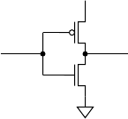
circuit components.) Figure 1.11 shows how such transistors are used
in a CMOS circuit for an inverter. When the input voltage is low, the
n-channel transistor at the bottom is turned off and the p-channel tran-
sistor at the top is turned on, pulling the output high. Conversely, when
the input voltage is high, the p-channel transistor is turned off and the
n-channel transistor is turned on, pulling the output low. Circuits for
other logic gates operate similarly, turning combinations of transistors
on or off to pull the output low or high, depending on the voltages at
the inputs.
1.3.2 LOGIC LEVELS
The first assumption we have made in the previous discussion is that
all signals take on appropriate “low” and “high” voltages, also called
logic levels, representing our chosen discrete values 0 and 1. But what
should those logic levels be? The answer is in part determined by the
characteristics of the electronic circuits. It is also, in part, arbitrary,
provided circuit designers and component manufacturers agree. As a
consequence, there are now a number of “standards” for logic levels.
One of the contributing factors to the early success of the TTL family
was its adoption of uniform logic levels for all components in the family.
These TTL logic levels still form the basis for standard logic levels in
modern circuits.
Suppose we nominate a particular voltage, 1.4V, as our threshold
voltage. This means that any voltage lower than 1.4V is treated as a “low”
voltage, and any voltage higher than 1.4V is treated as a “high” voltage.
In our circuits in preceding figures, we use the ground terminal, 0V, as
our low voltage source. For our high voltage source, we used the positive
power supply. Provided the supply voltage is above 1.4V, it should be
satisfactory. (5V and 3.3V are common power supply voltages for digital
systems, with 1.8V and 1.1V also common within ICs.) If components,
such as the gates in Figure 1.5, distinguish between low and high volt-
ages based on the 1.4V threshold, the circuit should operate correctly. In
the real world, however, this approach would lead to problems. Manufac-
turing variations make it impossible to ensure that the threshold volt-
age is exactly the same for all components. So one gate may drive only
slightly higher than 1.4V for a high logic level, and a receiving gate with
outputinput
+V
FIGURE 1.11 CMOS circuit
for an inverter.
1.3 Real-World Circuits
CHAPTER ONE 11
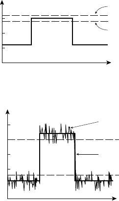
12 CHAPTER ONE introduction and methodology
0.5V
1.0V
1.5V
nominal 1.4V threshold
receiver threshold
FIGURE 1.12 Problems due
to variation in threshold voltage.
The receiver would sense the
signal as remaining low.
0.5V
1.0V
1.5V
2.0V
2.5V
logic low threshold
logic high threshold
driven signal
signal with added noise
FIGURE 1.13 Problems due
to noise on wires.
a threshold a little more above 1.4V would interpret the signal as a low
logic level. This is shown in Figure 1.12.
As a way of avoiding this problem, we separate the single thresh-
old voltage into two thresholds. We require that a logic high be greater
than 2.0V and a logic low be less than 0.8V. The range in between these
levels is not interpreted as a valid logic level. We assume that a signal
transitions through this range instantaneously, and we leave the behav-
ior of a component with an invalid input level unspecified. However,
the signal, being transmitted on an electrical wire, might be subject to
external interference and parasitic effects, which would appear as voltage
noise. The addition of the noise voltage could cause the signal voltage to
enter the illegal range, as shown in Figure 1.13, leading to unspecified
behavior.
The final solution is to require components driving digital signals to
drive a voltage lower than 0.4V for a “low” logic level and greater than
2.4V for a “high” logic level. That way, there is a noise margin for up to
0.4V of noise to be induced on a signal without affecting its interpretation
as a valid logic level. This is shown in Figure 1.14. The symbols for the
voltage thresholds are
V
OL
: output low voltage—a component must drive a signal with a
voltage below this threshold for a logic low
V
OH
: output high voltage—a component must drive a signal with a
voltage above this threshold for a logic high
왘
왘
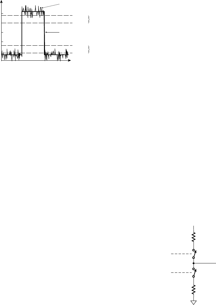
V
IL
: input low voltage—a component receiving a signal with a
voltage below this threshold will interpret it as a logic low
V
IH
: input high voltage—a component receiving a signal with a
voltage above this threshold will interpret it as a logic high
The behavior of a component receiving a signal in the region between
V
IL
and V
IH
is unspecified. Depending on the voltage and other factors,
such as temperature and previous circuit operation, the component may
interpret the signal as a logic low or a logic high, or it may exhibit some
other unusual behavior. Provided we ensure that our circuits don’t violate
the assumptions about voltages for logic levels, we can use the digital
abstraction.
1.3.3 STATIC LOAD LEVELS
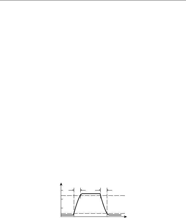
A second assumption we have made is that the current loads on compo-
nents are reasonable. For example, in Figure 1.3, the gate output is acting
as a source of current to illuminate the lamp. An idealized component
should be able to source or sink as much current at the output as its load
requires without affecting the logic levels. In reality, component outputs
have some internal resistance that limits the current they can source or
sink. An idealized view of the internal circuit of a CMOS component’s
output stage is shown in Figure 1.15. The output can be pulled high by
closing switch SW1 or pulled low by closing switch SW0. When one
switch is closed, the other is open, and vice versa. Each switch has a series
resistance. (Each switch and its associated resistance is, in practice, a
transistor with its on-state series resistance.) When SW1 is closed, current
is sourced from the positive supply and flows through R1 to the load con-
nected to the output. If too much current flows, the voltage drop across
R1 causes the output voltage to fall below V
OH
. Similarly, when SW0 is
closed, the output acts as a current sink from the load, with the current
flowing through R0 to the ground terminal. If too much current flows in
this direction, the voltage drop across R0 causes the output voltage to rise
above V
OL
. The amount of current that flows in each case depends on the
왘
왘
output
R1
SW1
SW0
R0
+V
FIGURE 1.15 An idealized
view of the output stage of a
CMOS component.
1.3 Real-World Circuits
CHAPTER ONE 13
0.5V
1.0V
1.5V
2.0V
2.5V
V
IL
V
OL
V
IH
V
OH
driven signal
noise margin
signal with added noise
noise margin
FIGURE 1.14 Logic level
thresholds with noise margin.

14 CHAPTER ONE introduction and methodology
output resistances, which are determined by component internal design
and manufacture, and the number and characteristics of loads connected
to the output. The current due to the loads connected to an output is
referred to as the static load on the output. The term static indicates that
we are only considering load when signal values are not changing.
The load connected to the AND gate in Figure 1.3 is a lamp, whose
current characteristics we can determine from a data sheet or from
measurement. A more common scenario is to connect the output of one
gate to the inputs of one or more other gates, as in Figure 1.5. Each
input draws a small amount of current when the input voltage is low and
sources a small amount of current when the input is high. The amounts,
again, are determined by component internal design and manufacture.
So, as designers using such components and seeking to ensure that we
don’t overload outputs, we must ensure that we don’t connect too many
inputs to a given output. We use the term fanout to refer to the number
of inputs driven by a given output. Manufacturers usually publish current
drive and load characteristics of components in data sheets. As a design
discipline when designing digital circuits, we should use that information
to ensure that we limit the fanout of outputs to meet the static loading
constraints.
example 1.3 The data sheet for a family of CMOS logic gates that
use the TTL logic levels described earlier lists the characteristics shown in
Table 1.1. Currents are specifi ed with a positive value for current fl owing into
a terminal and a negative value for current fl owing out of a terminal. The
parameter test condition min max
V
IH
2.0V
V
IL
0.8V
I
IH
5A
I
IL
5A
V
OH
I
OH
12mA
2.4V
I
OH
24mA
2.2V
V
OL
I
OL
12mA
0.4V
I
OL
24mA
0.55V
I
OH
24mA
I
OL
24mA
TABLE 1.1 Electrical
characteristics of a family
of logic gates.
parameters I
IH
and I
IL
are the input currents when the input is at a logic high
or low, respectively, and I
OH
and I
OL
are the static load currents at an output
driving logic high or low, respectively. What is the maximum fanout for an
output driving multiple inputs using this logic family, taking account of static
loading only?
solution For both high and low logic levels, an output can source or sink
up to 24mA of current, and an input load is 5A. Thus each output can drive
up to 24mA/5A 4800 inputs. However, in sourcing that much current in the
high level, the output voltage may drop to 2.2V, and in the low level, the output
voltage may rise to 0.55V. This gives a noise margin of only 0.2V for a high level
and 0.15V for a low level. If we want to preserve our 0.4V noise margins, we
need to limit the output currents to 12mA, in which case the maximum fanout
would be 2400 inputs.
In practice, we cannot connect anywhere near as many inputs to an
output as this example might suggest. Static loading is only one factor
that determines maximum fanout. In the next part of this section, we
will describe another factor that limits fanout more significantly in most
designs.
1.3.4 CAPACITIVE LOAD AND PROPAGATION DELAY
A further assumption we’ve made in the preceding discussion has been
that signals change between logic levels instantaneously. In practice, level
changes are not instantaneous, but take an amount of time that depends
on several factors that we shall explore. The time taken for the signal
voltage to rise from a low level to a high level is called the rise time,
denoted by t
r
, and the time for the signal voltage to fall from a high level
to a low level is called the fall time, denoted by t
f
. These are illustrated in
Figure 1.16.
One factor that causes signal changes to occur over a nonzero time
interval is the fact that the switches in the output stage of a digital com-
ponent, illustrated in Figure 1.15, do not open or close instantaneously.
Rather, their resistance changes between near zero and a very large value
over some time interval. However, a more significant factor, especially
in CMOS circuits, is the fact that logic gates have a significant amount
of capacitance at each input. Thus, if we connect the output of one
1.0V
2.0V
3.0V
V
OL
V
OH
t
r
t
f
FIGURE 1.16 Rise time and
fall time for a signal whose value
is changing.
1.3 Real-World Circuits
CHAPTER ONE 15

16 CHAPTER ONE introduction and methodology
output
input
C
in
R1
SW1
SW0
R0
+V
FIGURE 1.17 Connection of
an output stage to a capacitively
loaded input.
component to the input of another, as shown in Figure 1.17, the input
capacitance must be charged and discharged through the output stage’s
switch resistances in order to change the logic level on the connecting
signal.
If we connect a given output to more than one input, the capacitive
loads of the inputs are connected in parallel. The total capacitive load
is thus the sum of the individual capacitive loads. The effect is to make
transitions on the connecting signal correspondingly slower. For CMOS
components, this effect is much more significant than the static load of
component inputs. Since we usually want circuits to operate as fast as
possible, we are constrained to minimize the fanout of outputs to reduce
capacitive loading.
A similar argument regarding time taken to switch transistors on and
off and to charge and discharge capacitance also applies within a digital
component. Without going into the details of a component’s circuit, we
can summarize the argument by saying that, due to the switching time
of the internal transistors, it takes some time for a change of logic level
at an input to cause a corresponding change at the output. We call that
time the propagation delay, denoted by t
pd
, of the component. Since the
time for the output to change depends on the capacitive load, component
data sheets that specify propagation delay usually note the capacitive load
applied in the test circuit for which the propagation delay was measured,
as well as the input capacitance.
example 1.4 For a collection of CMOS gate components, the manufacturer’s
data sheet specifi es a typical input capacitance, C
in
, of 5pF. The AND gate compo-
nent has a maximum propagation delay, t
pd
, of 4.3ns measured with a load capaci-
tance, C
L
, of 50pF. What is the maximum fanout for the AND gate that can be used
without causing the propagation delay to exceed the specifi ed maximum?

solution Allowing only for the capacitive loading effect of the inputs, the
maximum fanout is
C
L
/ C
in
50pF / 5pF 10
In practice, other stray capacitance between the output and the inputs would
limit the maximum fanout to a smaller value.
In many components, the propagation delay differs depending on
whether the output is changing from 0 to 1 or from 1 to 0. If it is impor-
tant to distinguish between the two cases, we can use the symbol t
pd01
for the propagation delay when the output changes from 0 to 1, and t
pd10
for
the propagation delay when the output changes from 1 to 0. If we don’t
need to make this distinction, we usually use the largest of the two values,
that is,
t
pd
max (t
pd01
, t
pd10
)
1.3.5 WIRE DELAY
Yet another assumption we’ve made about the behavior of digital systems
is that a change in the value of a signal at the output of a component
is seen instantaneously at the input of other connected components. In
other words, we’ve assumed that wires are perfect conductors that propa-
gate signals with no delay. For very short wires, that is, wires of a few
centimeters on a circuit board or up to a millimeter or so within an IC,
this assumption is reasonable, depending on the speed of operation of the
circuit. For longer wires, however, we need to take care when designing
high-speed circuits. Problems can arise from the fact that such wires have
parasitic capacitance and inductance that are not negligible and that delay
propagation of signal changes. Such wires should be treated as transmis-
sion lines and designed carefully to avoid unwanted effects of reflection of
wavefronts from stubs and terminations. A detailed treatment of design
techniques in these cases is beyond the scope of this book. However, we
need to be aware that relatively long wires add to the overall propagation
delay of a circuit. Later, we will describe the use of computer-based tools
that can help us to understand the effects of wire delays and to design our
circuits appropriately.
1.3.6 SEQUENTIAL TIMING
In our discussion of sequential digital systems in Section 1.2, we assumed
that a flip-flop stores the value of its data input at the moment the clock
input rises from 0 to 1. Moreover, we assumed that the stored value is
reflected on the output instantaneously. It should not be surprising now
1.3 Real-World Circuits CHAPTER ONE 17

18 CHAPTER ONE introduction and methodology
that these assumptions are an abstraction of realistic sequential circuit
behavior, and that we must observe design disciplines to support the
abstraction. Real flip-flops require that the value to be stored be present
on the data input for an interval, called the setup time, before the rising
clock edge. Also, the value must not change during that interval and for
an interval, called the hold time, after the clock edge. Finally, the stored
value does not appear at the output instantaneously, but is delayed by an
interval called the clock-to-output delay. These timing characteristics are
shown in Figure 1.18. In this timing diagram, we have drawn the rising
and falling edges as sloped, rather than vertical, to suggest that the transi-
tions are not instantaneous. We have also drawn both 0 and 1 values for
the data input and output, suggesting that it is not the specific values that
are relevant, but the times at which values change, shown by the coinci-
dent rising and falling values. The diagram illustrates the constraint that
changes on the data input must not occur within a time window around
the clock rising edge, and that the data output cannot be assumed correct
until after some delay after the clock edge.
In most sequential digital circuits, the output of one flip-flop is either
connected directly to the data input of another, or passes through some
combinational logic whose output is connected to the data input of another
flip-flop. In order for the circuit to operate correctly, a data output result-
ing from one clock edge must arrive at the second flip-flop ahead of a setup
interval before the next clock edge. This gives rise to a constraint that we
can interpret in two ways. One view is that the delays in the circuit between
flip-flops are fixed and place an upper bound on the clock cycle time, and
hence on the overall speed at which the circuit operates. The other view is
that the clock cycle time is fixed and places an upper bound on the permissi-
ble delays in the circuit between flip-flops. According to this view, we must
ensure that we design the circuit to meet that constraint. We will examine
timing constraints for sequential circuits in much more detail in Chapter 4,
and describe a design discipline that ensures that we meet the constraints,
thus allowing us to use the timing abstraction of periodic clock cycles.
1.3.7 POWER
Many modern applications of digital circuits require consideration of
the power consumed and dissipated. Power consumption arises through
current being drawn from a constant-voltage power supply. All gates and
other digital electronic components in a circuit draw current to operate the
transistors in their internal circuitry, as well as to switch input and output
transistors on and off. While the current drawn for each gate is very small,
the total current drawn by millions of them in a complete system can be
many amperes. When the power supply consists of batteries, for example,
in portable appliances such as phones and notebook computers, reducing
power consumption allows extended operating time.
t
su
t
out
t
h
D
clk
Q
FIGURE 1.18 Setup, hold
and clock-to-output times for a
fl ip-fl op.
The electrical power consumed by the current passing through
resistance causes the circuit components to heat up. The heat serves no
useful purpose and must be exhausted from the circuit components.
Designers of the physical packaging of ICs and complete electronic
systems determine the rate at which thermal energy can be transferred
to the surroundings. As circuit designers, we must ensure that we do not
cause more power dissipation than can be handled by the thermal design,
otherwise the circuit will overheat and fail. Puffs of blue smoke are the
usual sign of this happening!
There are two main sources of power consumption in modern digital
components. The first of these arises from the fact that transistors, when
turned off, are not perfect insulators. There are relatively small leakage
currents between the two terminals, as well as from the terminals to
ground. These currents cause static power consumption. The second
source of power consumption arises from the charging and discharging of
load capacitance when outputs switch between logic levels. This is called
dynamic power consumption. To a first approximation, the static power
consumption occurs continuously, independent of circuit operation,
whereas dynamic power consumption depends on how frequently signals
switch between logic levels.
As designers, we have control over both of these forms of power
consumption. We can control static power consumption of the circuit by
choosing components with low static power consumption, and, in some
cases, by arranging for parts of circuits that are not needed for periods
of time to be turned off. We can control dynamic power consumption by
reducing the number and frequency of signal transitions that must occur
during circuit operation. This is becoming an increasingly important part
of the design activity, and computer-based tools for power analysis are
gaining increased use. We will discuss the topic of power analysis in more
detail throughout this book.
1.3.8 AREA AND PACKAGING
In most applications of digital electronics, cost of the final manufactured
product is an important factor, particularly when the product is to be sold
in a competitive market. There are numerous factors that influence cost,
many of them based on business decisions rather than engineering design
decisions. However, one factor over which designers have control and
that strongly affects the final product cost is circuit area.
As we mentioned earlier, digital circuits are generally implemented as
integrated circuits, in which transistors and wires are chemically formed
on the surface of a wafer of crystalline silicon (see Figure 1.19). The more
transistors and wires in our circuit, the more surface area it consumes.
The manufacturing process for ICs is based on wafers of a fixed size, up
to 300mm in diameter, with a fixed cost of manufacture. Multiple ICs
FIGURE 1.19 A silicon
wafer, on which multiple ICs are
manufactured.
1.3 Real-World Circuits
CHAPTER ONE 19
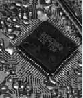
20 CHAPTER ONE introduction and methodology
are manufactured on a single wafer in a series of steps. The wafer is then
broken into individual ICs, which are encapsulated in packages that can
be soldered onto the circuit board of a complete system (see Figure 1.20).
Thus, the larger the individual IC, the fewer there are per wafer, and so the
greater their cost. Unfortunately, the manufacturing process is not perfect,
so defects occur, distributed across the surface of the wafer. Those ICs that
have a defect that cause them not to function correctly are discarded. Since
the cost of manufacturing a wafer is fixed, the functional ICs must bear
the cost of those that are nonfunctional, increasing the final product cost
of the IC. The larger an individual IC, the greater the proportion that have
defects. So the final cost of an IC is disproportionately dependent on area.
Since each IC is packaged individually, the cost of the package is a
direct cost of the final product. The package serves two purposes. One is
to provide connection pins, allowing the wires of the IC to be connected
to external wires in the larger digital system, as well as providing for
power supply and ground connections. An IC with more external con-
nections requires more pins and, thus, a more costly package. Therefore,
the pin count of the IC is a factor that constrains our designs. The other
purpose served by the IC package is to transfer heat from the IC to the
surroundings so that the IC does not overheat. If the IC generates more
thermal power than the package can dissipate, additional cooling devices,
such as heat sinks, fans or heat pipes, are required, adding to cost. Thus,
thermal concerns arising from packaging also constrain our designs.
As we have suggested, a packaged IC may not be the final product
of a design. The IC may be one of several components on a printed cir-
cuit board, which, in turn, is assembled with other items into a complete
packaged product. Similar arguments to those above can be made about
the cost of a printed circuit board based on the number of ICs and other
components, the number of external connections, the area or size of the
board and package, and heat dissipation in the enclosing case or cabinet.
1. What are the TTL output voltage levels, input threshold voltages
and noise margins?
2. What is meant by the term fanout?
3. How is the propagation delay of a component defi ned?
4. Why do we try to minimize fanout of components?
5. Do wires contribute to delay in a circuit?
6. What is meant by the terms setup time, hold time and clock-to-output
time of a fl ip-fl op?
7. What are the two sources of power consumption in a digital component?
8. Is the cost of an IC proportional to the area of the IC?
KNOWLEDGE
TEST QUIZ
KNOWLEDGE
TEST QUIZ
FIGURE 1.20 A packaged
IC soldered onto a printed circuit
board.
1.4 MODELS
As children, many of us will have made or played with models of real-world
things, for example, model airplanes. One way of thinking of a model
is that it is a representation of an object that incorporates aspects of
interest for a particular purpose while omitting aspects that are not rel-
evant. In other words, it is an abstraction of an object. A model airplane
may, for example, have the look of a real airplane, but does not have
the scale or detailed mechanical aspects of the real thing. The model
incorporates just those aspects that satisfy a child’s wish to play with an
airplane.
Now that we’ve grown up (mostly!) and turned to digital circuit
design, our task is to design circuits that perform certain required func-
tions while meeting various constraints. We could try to build a prototype
circuit to check that it performs as required, but that would be costly and
time consuming, since we would usually need to work through numer-
ous versions before we get things right. A more effective approach is to
develop models of our designs and to evaluate them. A model of a digital
circuit is an abstract expression in some modeling language that captures
those aspects that we are interested in for certain design tasks and omits
other aspects. For example, one form of model may express just the func-
tion that the circuit is to perform, without including aspects of timing,
power consumption or physical construction. Another form of model
may express the logical structure of the circuit, that is, the way in which
it is composed of interconnected components such as gates and flip-flops.
Both of these forms of model may be conveniently expressed in a hard-
ware description language (HDL), which is a form of computer language
akin to programming languages, specialized for this purpose.
Functional models may also be expressed in mathematical notations,
such as Boolean equations and finite state machine notations, that we will
introduce in later chapters. Structural models may also be expressed in
the form of graphical circuit schematics, such as those in earlier figures in
this chapter. We will use all of these forms of models where appropriate,
but we will focus on models expressed in an HDL, since that allows us
to take advantage of computer-aided design (CAD) tools to help us with
design tasks. Designing electronic circuits using CAD tools is also called
electronic design automation (EDA).
In this book, we will introduce and use an HDL called Verilog. Verilog
was originally developed by Phil Moorby at a company called Gateway
Design Automation, which was subsequently acquired by Cadence Design
Systems. Since then, the specification of Verilog has been standardized in
the United States by the Institute of Electrical and Electronic Engineers
(IEEE) and internationally by the International Electrotechnical Commis-
sion (IEC), and the language has been widely adopted by designers and
tool developers.
1.4 Models CHAPTER ONE 21

22 CHAPTER ONE introduction and methodology
Verilog is not the only HDL used for digital system design. The other
main HDL in widespread use is VHDL. Fairly recently, SystemVerilog has
been developed as an extension to Verilog, aimed at design and verification
of complex digital systems. Also, SystemC, an extension of the C
programming language, is gaining increased usage. While these languages
have many basic features in common, they vary in their more advanced
features. Moreover, they are all evolving, with new features being added
in successive revisions to meet evolving design challenges. Choice among
them is often dictated by tool availability and organizational culture, as
well as the kind of design work to be performed.
example 1.5 Develop a Verilog model that expresses the logical structure
of the gate circuit in Figure 1.5. Assume that the sensor signals and the switch
signal are inputs to the model, and that the buzzer signal is the output from the
model.
solution The Verilog model consists of a module definition, describing
the inputs and output of the circuit and the implementation of the circuit:
module vat_buzzer_struct
( output buzzer,
input above_25_0, above_30_0, low_level_0,
input above_25_1, above_30_1, low_level_1,
input select_vat_1 );
wire below_25_0, temp_bad_0, wake_up_0;
wire below_25_1, temp_bad_1, wake_up_1;
// components for vat 0
not inv_0 (below_25_0, above_25_0);
or or_0a (temp_bad_0, above_30_0, below_25_0);
or or_0b (wake_up_0, temp_bad_0, low_level_0);
// components for vat 1
not inv_1 (below_25_1, above_25_1);
or or_1a (temp_bad_1, above_30_1, below_25_1);
or or_1b (wake_up_1, temp_bad_1, low_level_1);
mux2 select_mux (buzzer, select_vat_1, wake_up_0, wake_up_1);
endmodule
The module in this case is named vat_buzzer_struct. The module has ports,
named in the port list of the module declaration. Each port is given a name
and is either an output or an input.
The remainder of the module definition contains the details of the circuit model.
In this case, the circuit is modeled as a collection of interconnected components.
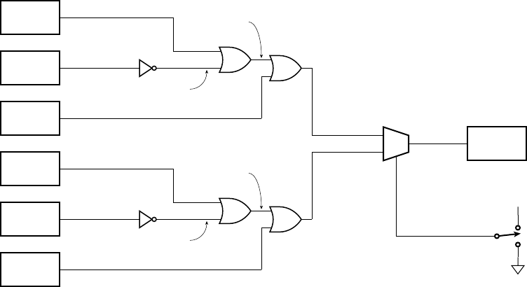
We use the term structural model to refer to a model in this form. A number of
named nets are declared, introduced by the keyword
wire, for connecting the
components together. In this case, Verilog would allow us to omit the net decla-
rations, since each net is a simple wire carrying just a 0 or 1 value. We introduce
the declarations in this example to illustrate where they can occur in a module,
but will omit them in subsequent examples where Verilog permits.
Following the net declarations are a number of instances. Each has a name to
distinguish it, and specifies which kind of component is instantiated. For example,
inv_0 is an instance of the not component, representing the inverter for vat 0 in
the circuit. Some components, such as the
or and not components, are built into
Verilog. Others, such as the
mux2 component, are defined as separate modules that
we instantiate. (The source code of the
mux2 module, along with other source code
and documentation, is provided on the companion website for this book.) Within
parentheses, the nets and circuit outputs and inputs connected to the ports of each
component are listed. For example, the inverter
inv_0 has the net below_25_0 con-
nected to its first port and the input
above_25_0 connected to its second port. The
built-in primitive components all have the output port first in the list, followed by
the input ports. When we write our own modules, we can choose the order of input
and output ports. However, in this book, we largely follow the convention of listing
output ports before input ports, for consistency with the built-in primitives.
We have also included some comments in this module to provide documentation.
One form of comment, shown here, starts with two slash characters and extends
to the end of the line. Another form starts with the characters /* and extends to the
characters */. This form can extend over more than one line. Figure 1.21 shows the
vat buzzer circuit again with the net and component names included for reference.
>30°C
low level
buzzer
>25°C
>30°C
low level
>25°C
0
1
above_25_0
below_25_0
temp_bad_0
below_25_1
above_30_0
inv_0
or_0a
or_1a
or_0b
select_mux
or_1b
inv_1
wake_up_0
wake_up_1
low_level_0
above_25_1
above_30_1
low_level_1
select_vat_1
buzzer
temp_bad_1
+V
FIGURE 1.21 The vat buzzer
circuit, showing net and component
names.
1.4 Models
CHAPTER ONE 23

24 CHAPTER ONE introduction and methodology
example 1.6 Develop a Verilog model that expresses the function per-
formed by the gate circuit in Figure 1.5.
solution We can use the same port list and port declarations as for the
structural model, since the inputs and outputs are the same. We simply need to
revise the body of the module:
module vat_buzzer_behavior
( output buzzer,
input above_25_0, above_30_0, low_level_0,
input above_25_1, above_30_1, low_level_1,
input select_vat_1 );
assign buzzer =
select_vat_1 ? low_level_1 | (above_30_1 | ~above_25_1)
: low_level_0 | (above_30_0 | ~above_25_0);
endmodule
A model of this form, in which we describe the function performed by the
circuit, is called a behavioral model. (Some people also use this term for more
abstract models of functionality, but in the absence of a better term, we will use
it as described here.) Within the module, we have a single assignment statement
that determines the value of the output port using the values of the input ports.
The operators
| and ~ correspond in function to the OR gates and inverters,
respectively, in the circuit. The choice of value to assign to the output port
depends on the condition in the
. . . ? . . . : . . . else construct, corresponding to
the multiplexer in the circuit. The value before the ? character is tested. If it
is 1, the value of the expression after the ? character is used, otherwise the value
after the : character is used.
The examples above illustrate the general organization of structural
and behavioral Verilog models. The Verilog tutorial and reference material
included on the companion website for this book provide more detailed
information on the specifics of writing Verilog models. The source code
for all of the example models in this book is also provided on the com-
panion website. We follow the convention of naming each source code file
after the module it contains. This makes it easier to locate the file contain-
ing a given model.
There are three principal design tasks that benefit from the use of
Verilog. The first of these is design entry, that is, expressing a model in a
form that can be input to a CAD tool. For simple circuits, design entry can
also be done using graphical schematics, and many CAD tools provide
for that form of input. However, schematics for larger and more complex
circuits can be cumbersome, particularly when they are annotated with
information such as the types of signals. Moreover, a textual form, such
as Verilog, allows for richer forms of expression, as we shall see in later
examples. It also works better with other computer tools, such as script-
ing tools and source-code control tools. For these reasons, we shall focus
on Verilog descriptions of circuits and use circuit schematics for illustra-
tive purposes in this book.
The second design task that benefits from use of Verilog is verification,
that is, ensuring that the design meets its requirements and constraints.
There are several aspects to verification. Functional verification involves
ensuring that the design performs the required function. Timing verifica-
tion involves ensuring that the design meets its timing constraints. Timing
constraints are ultimately derived from the performance requirements of
the circuit. For example, in a circuit that processes a digital representation
of an audio signal, the processing steps must be performed at the sam-
pling rate of the signal. Other verification tasks include power verifica-
tion (ensuring that the circuit meets power consumption and dissipation
constraints); manufacturability verification (ensuring that the circuit will
operate correctly for all variations that might arise in the manufacturing
processes); and test verification (ensuring that the manufactured circuit
can be tested to identify defective parts). All of these forms of verification
involve analysis of models of the circuit to determine the relevant proper-
ties and checking that the property values are acceptable.
Functional verification is often the most time consuming part of the
entire design process. One approach to functional verification is simula-
tion, in which the model is interpreted as an executable computer program
by a CAD tool called a simulator. This involves applying different com-
binations and sequences of values to the input ports, executing the model
code, and ensuring that it produces the required values on the output ports.
For behavioral models, the expressions in assignment statements can be
executed directly. For structural models, each component instance must
have a corresponding behavioral model that can be invoked by the simula-
tor. The simulator passes values produced at the outputs of components
along the interconnecting signals to the inputs of other components.
The problem with simulation, particularly for large and complex
models, is that covering all possible combinations and sequences of values
that might arise in the real circuit is time consuming and resource inten-
sive, and is generally not feasible. An alternative to simulation is formal
verification, which involves mathematical proof of properties of the
design. The properties take the form of logical statements relating values
of inputs and outputs, or sequences of values of inputs and outputs, that
express the functional requirements, usually in a more abstract form than
that of the model being verified. The analysis of the model and proof
of the properties is performed by a CAD tool called a model checker.
Formal verification is a relatively new technology, and can require
significant computational resources. In practice, functional verification of
1.4 Models CHAPTER ONE 25
26 CHAPTER ONE introduction and methodology
real-world circuits is most effectively done using a combination of simula-
tion and formal verification. We will return to this issue in more detail in
our discussions of design methodology in Section 1.5 and Chapter 10.
The third design task that benefits from use of Verilog is synthesis.
This involves automatic refinement and optimization of a model at
a higher level of abstraction into a structural model at a lower level of
abstraction. For example, the register transfer level (RTL) of abstraction
in Verilog involves expressing behavior in terms of assignment statements
and expressions, such as those in Example 1.6, as well as procedural
blocks, that we shall come to later. An RTL synthesis CAD tool automati-
cally refines an RTL model into an optimized gate-level model, that is,
a structural model using gate components such as that of Example 1.5.
Since a synthesis tool automates a task that we would otherwise have to
perform manually, it greatly improves our productivity. In particular, it
makes more complex designs tractable.
Since hardware description languages such as Verilog help so signifi-
cantly with these design tasks, they have become central to modern design
methods. Throughout this book, as we introduce digital components and
circuits, we will also show Verilog models that describe them. As we intro-
duce design methods, we will show how CAD tools that process models
help us perform these methods.
1. What does a Verilog module defi ne?
2. What information is specifi ed for each port in a Verilog module?
3. What is meant by the terms structural model and behavioral
model?
4. What are functional verifi cation and timing verifi cation?
5. Identify two approaches to functional verifi cation.
6. What is meant by synthesis?
1.5 DESIGN METHODOLOGY
Designing a digital system of any significant complexity is a large under-
taking, requiring a systematic approach. This is especially important
when many people are collaborating on a design, as is usually the case.
Depending on the complexity of the product, design teams can range in
size from a handful of engineers for a relatively simple product, to several
hundred people for a complex IC or packaged system. We use the term
design methodology to refer to the systematic process of design, verifica-
tion and preparation for manufacture of a product. A design methodology
specifies the tasks undertaken, the information required and produced by
KNOWLEDGE
TEST QUIZ
KNOWLEDGE
TEST QUIZ
each task, the relationships between the tasks, including dependencies and
sequencing, and the CAD tools used. A mature design methodology will
also be reflective, specifying measurements that will be made of the design
process, such as adherence to schedule and budget, and numbers of design
errors detected and missed. Accumulated data from previous projects can
be used to improve the design methodology for subsequent projects. The
benefit of a good methodology is that it makes the design process more
reliable and predictable, thus reducing risk and cost. Even a small design
project benefits from a design methodology, though perhaps on a reduced
scale.
Given its importance, we will focus on design methodology through-
out this book. We will start by outlining a relatively simple methodology,
since we are in the early stages of learning digital design. In Chapter 10,
we will see what’s involved in a more complete methodology for real-
world systems.
Figure 1.22 illustrates a simple design methodology. The starting
point is a collection of requirements and constraints. These are usually
generated externally to the design team, for example, by the marketing
group of a company or by a customer for whom a product develop-
ment is undertaken. They usually include function requirements (what
the product is to do), performance requirements (how fast it is to do
it), and constraints on power consumption, cost and packaging. The
design methodology specifies three tasks—design, synthesis and physical
implementation—each of which is followed by a verification task. (The
design and functional verification tasks are outlined to indicate that they
are actually a bit more involved than is shown on the diagram. We will
come back to this shortly.) If verification fails at any stage, we must revisit
a previous task to correct the error. Ideally, we would like to revisit only
the immediately preceding task and make a minor correction. However,
if the error is severe enough, we may need to backtrack further to make
more significant changes. Hence, when performing a given design task, it
is worth keeping in mind the constraints applying in subsequent tasks, so
as to avoid introducing errors that will be detected later. Once the tasks
and associated verification activities have been performed, the product
can be manufactured, and each unit tested to ensure that it is functional.
We will now spend a little time examining the stages in this methodology
in more detail.
The design task involves understanding the requirements and con-
straints and developing a specification of a digital circuit that meets the
requirements and constraints. The information produced by this task is
a collection of models that describe the design. The methodology then
specifies that we verify the function of the design, using techniques such
as simulation and formal verification. In preparation for the verification
task, we should prepare a verification plan that identifies what input and
output cases should be verified, and what CAD tools should be used. We
Requirements
and
Constraints
Design
N
Y
N
Y
N
Y
Functional
Verification
OK?
Synthesize
Post-Synthesis
Verification
OK?
Physical
Implementation
Physical
Verification
Manufacture
Test
OK?
FIGURE 1.22 A simple
design methodology.
1.5 Design Methodology
CHAPTER ONE 27
28 CHAPTER ONE introduction and methodology
will illustrate development of verification plans in parallel with design
tasks throughout this book.
We’ve already discussed use of abstractions to make the design task
more manageable, and the need to adhere to design disciplines to ensure
that we don’t violate assumptions underlying the abstractions. However,
for a system of any significant complexity, that is still not sufficient to
make the task tractable. Another form of abstraction that allows us to
manage design complexity is hierarchical composition. This involves
developing a subcircuit that performs some relatively simple function,
then treating it as a “black box.” Provided we adhere to assumptions
made in designing the subcircuit, we can then use it in a larger circuit
that performs a more complex function. As an example, the subcircuit
might be a small liquid-crystal display (LCD) controller, which is used as
part of the user interface of a cordless phone. We can repeat the step of
using one subcircuit as part of a more complex circuit. For example, the
user-interface subcircuit might be used as a black box within the cordless
phone handset. At each level of the hierarchical design, we can focus on
the aspects that are relevant and hide the details of the lower-level compo-
nents. Using abstraction in this way makes the task of designing complex
systems tractable. It also allows us to re-use subcircuits, either from previ-
ous projects or from third-party providers. Design re-use can potentially
save significant design effort and cost.
Hierarchical composition in a design also makes functional verifica-
tion more tractable. We can first verify each of the most primitive subcir-
cuits as independent units. Next, we can verify a subsystem that uses the
subcircuits by treating the subsystem as a collection of black boxes. In
particular, we can use more abstract models of the black box subcircuits
instead of detailed models that describe their internal composition. This
approach means that the verification tools have less work to do, allowing
them to verify more input/output cases for the subsystem. We can repeat
this process until we have verified the entire system.
Returning to the design and verification tasks shown in Figure 1.22,
we can expand the design and functional verification tasks to illustrate
use of hierarchical composition, as shown in Figure 1.23. This approach
is often called top-down design. Architectural design involves analyzing
the requirements and developing the overall organization of a digital
system to meet them. One of the main tools used for this level of design
is a white board, on which system architects draw (and redraw) block
diagrams describing the main subsystems and their interconnections. The
next step is unit design, in which the subsystems and sub-subsystems are
designed. Each unit can then be verified, possibly requiring some rede-
sign if any of the units fail verification. Finally, the units can be inte-
grated and the subsystems and entire system verified, as we described
above. Again, if verification fails, units may need to be redesigned. If the
Unit
Design
Unit
Verification
Architecture
Design
OK?
Integration
Verification
OK?
N
Y
N
Y
FIGURE 1.23 Hierarchical
design and verifi cation.
failure is severe enough, it may be necessary to revise the architectural
organization of the system, and then to reflect the changes in the unit
designs.
The tasks immediately after functional verification in the design
methodology of Figure 1.22 are synthesis and post-synthesis verification.
We described synthesis in the previous section as automatic refinement
and optimization of a model at a higher level of abstraction to a structural
model at a lower level of abstraction. Currently, synthesis is usually per-
formed from register-transfer level to gate level, as CAD tool technology
for this level of refinement is quite mature. Behavioral synthesis (also
called high-level synthesis), from higher levels of abstraction to RTL, is
much less mature, though the subject of much active development work.
In order to perform RTL synthesis, we specify information about the
implementation fabric that we intend to use for our design. We might also
annotate the RTL models with additional information to guide the syn-
thesis CAD tool in its optimization task. The tool then selects primitive
components from a library of components available in the chosen imple-
mentation fabric and constructs a circuit with the same function as that
of the RTL design. The library may contain further information about the
properties of each component, such as timing parameters, power dissipa-
tion, and so on. Our design methodology shows that we use this informa-
tion, together with the refined design produced by the synthesis tool, to
further verify the design. Using the timing parameters and the information
about the way components are interconnected, a static timing analysis tool
can estimate propagation delays in the circuit and verify that timing con-
straints are met. Similarly, using information about the number or transis-
tors and amount of wiring required for components, a floor planning tool
can estimate the area of the design and verify that area and packaging
constraints are met. Note that the properties used at this stage are esti-
mates of final property values for the manufactured circuit, and need to
be refined later in the design process. As a further step in verification, an
equivalence checker can compare the function of the refined design with
that of the original RTL design to verify that the synthesis tool has done its
job correctly and that the functional requirements are still met.
The next task in the design methodology is physical implementation.
This involves using the refined design, expressed as an interconnection
of primitive circuit elements, and generating the information required to
manufacture the circuit. The precise steps to be performed depend on the
implementation fabric chosen for the circuit. By implementation fabric,
we mean the kind of IC used to implement a design. The two main imple-
mentation fabrics in common use today are field-programmable gate
arrays (FPGAs) and application-specific integrated circuits (ASICs). An
FPGA consists of a large number of gates and flip-flops whose intercon-
nection can be determined, or programmed, after the IC is manufactured.
1.5 Design Methodology CHAPTER ONE 29
30 CHAPTER ONE introduction and methodology
In this book, we will focus on FPGAs, especially in lab projects, since they
are widely used for a range of circuits of varying size and complexity, can
be reprogrammed, and are cost-effective for nearly all but large-volume
applications. ASICs, as their name suggests, are ICs that are customized
for a particular application, and cannot be programmed. We will describe
these implementation fabrics in more detail in Chapter 6. However, for
now, we can identify some general steps that are common to physical
implementation on both of these fabrics, as well as on printed circuit
boards.
The first of these steps is mapping, which involves determining the
particular circuit resources to be used for each of the components in
the refined design. Next, placement and routing determines where each
mapped component is to be positioned in the physical circuit and where
the interconnecting wires run. Once mapping, placement and routing are
done, refined estimates of circuit properties can be extracted. In particu-
lar, since the physical wiring details have been determined, propagation
delays through wires can be included in the timing estimates. These refined
estimates are used to perform final physical verification. Finally, one or
more files of information are generated for manufacturing the circuit.
When that step is passed, we reach a golden milestone, called tape out
for ASIC design, referring historically to production of a magnetic tape
containing the manufacturing data to be shipped out to the manufacturer.
These days, the data is more likely to be transferred by file transfer over
the Internet. Nonetheless, reaching the milestone is usually reason for the
design team to hold a party!
The final tasks shown in the design methodology are the manufactur-
ing and test tasks. For ASICs, manufacturing is done by a foundry that
uses the design information to control the chemical processes that form
ICs on silicon wafers. For FPGAs, prefabricated parts are programmed
using the design information. In your lab work, you will encounter the
CAD tools and equipment needed to program FPGAs. The test task for
ASICs involves exercising each manufactured circuit to ensure that it
operates correctly. Some parts, as we’ve mentioned, will fail to operate
due to defects in their manufacture and must be discarded. Alternatively,
all of the manufactured parts may fail due to design errors that escaped
the various verification steps we performed. Identifying the errors that
cause such failures is very difficult and costly, involving use of measuring
instruments to probe wires within the circuit to trace actual operation.
It is much better to avoid bug escapes by verifying the design more thor-
oughly earlier in the design process. Testing of FPGA ICs also occurs once
they are manufactured, but before they are delivered to customers for
programming. Once an FPGA has been programmed, the programming
device will often read back the program to verify that it has been correctly
installed.
1.5.1 EMBEDDED SYSTEMS DESIGN
In Section 1.1 we introduced the idea of an embedded system, a digital
system in which one or more computers are used as components. Each
embedded computer comprises a processor core, memory and interfaces
with other parts of the system. Since the computers must be programmed
to implement part of the system’s functionality, we must augment our
design methodology to include embedded software design.
Recall that the initial inputs to the design methodology are the
functional requirements and constraints for the system. As part of our
architectural design considerations, we can choose which aspects of
functionality can be implemented by embedded software on a processor
core, and which parts can be implemented as digital subcircuits, that is,
by hardware. Designing the hardware and software for a system together
is called hardware/software codesign. Deciding which parts to put in
hardware and which in software is called partitioning. There are numer-
ous trade-offs to consider. Functionality that involves testing many
conditions and taking alternative actions can be hard to implement in
hardware, but is relatively straightforward in software. On the other
hand, functionality that involves performing rapid computations on
large amounts of data or data that arrives at a high rate may need a very
high performance (and hence costly and power hungry) processor core,
and so may more readily be performed by customized hardware. A fur-
ther consideration is that embedded software may be stored in memory
circuits that may be reprogrammed after the system is manufactured or
deployed. Thus, the software may be upgraded to correct design errors
or add functionality without revising the hardware design or replacing
deployed systems.
Once functionality has been partitioned between hardware and
software, development of the two can proceed concurrently, as shown
in Figure 1.24. For those aspects of the embedded software that depend
on hardware, the abstract behavioral models from the hardware design
task can be used to verify the software design. This can be done using an
instruction-set simulator for the processor core working in tandem with
a simulator for the hardware model. A similar approach can be used to
verify parts of the hardware that interface directly with a processor core.
Test programs can be run using the processor simulator running in tan-
dem with the hardware simulator. The benefits of developing hardware
and software concurrently include avoiding the extra time involved in
developing one after the other, and early detection of errors in the inter-
play of software and hardware.
1. What is meant by the term design methodology?
2. Why is a design methodology benefi cial?
KNOWLEDGE
TEST QUIZ
KNOWLEDGE
TEST QUIZ
1.5 Design Methodology CHAPTER ONE 31
32 CHAPTER ONE introduction and methodology
3. If verifi cation fails during some stage of a design methodology, what
action is taken?
4. What is meant by top-down design?
5. Name two implementation fabrics for digital circuits.
6. What is an embedded system?
7. What is meant by the term hardware/software codesign?
Requirements
and
Constraints
Partitioning
N
YY
Hardware
Verification
Hardware
Requirements and
Constraints
Software
Requirements and
Constraints
Hardware
Design
Software
Verification
Software
Design
OK? OK?
Manufacture
Test
N
FIGURE 1.24 A design
methodology for hardware/
software codesign.

1.6 CHAPTER SUMMARY
Abstraction means identifying aspects that are important to a task at
hand and hiding details of other aspects. Using abstractions requires
following design disciplines to avoid violating assumptions inherent
in the abstractions.
The digital abstraction considers voltages to be high or low logic
levels, and time to be a sequence of intervals called clock periods.
Binary representation uses bits (0 and 1) to represent logical condi-
tions. These can be implemented in a circuit using low and high logic
levels.
Logic gates are circuit elements that implement logical operations on
binary-represented information. Logic gates can be interconnected in
a circuit to perform more complex logical functions.
Combinational circuits are those whose outputs depend only on the
current values of inputs. They do not include any storage of informa-
tion. Sequential circuits are those whose outputs depend on current
and past input values. They include storage elements.
A flip-flop is a storage element that stores one bit of information.
An edge-triggered flip-flop stores the value of its input when a clock
input changes, that is, when a clock edge occurs.
The output low voltage of a driver is lower than the input low
threshold of a receiver, and the output high voltage of a driver is
higher than the input high threshold of a receiver. The differences are
called the noise margins.
Static and capacitive loading limits the fanout of a driver, that is, the
number of inputs that can be connected to the output.
Propagation delay depends on delay within components, capacitive
loading and wire delays. Flip-flops have setup and hold time win-
dows and clock-to-output delays.
Circuits consume and dissipate static power, due to current leakage,
and dynamic power, due to switching between logic levels.
Circuit area and packaging have significant effects on cost.
A model written in a hardware description language allows us to
enter a design description into CAD tools, to verify it (using simula-
tion and formal verification), and to synthesize it.
A behavioral model describes the function performed by a circuit.
A structural model describes the circuit as an interconnection of
components.
왘
왘
왘
왘
왘
왘
왘
왘
왘
왘
왘
왘
왘
1.6 Chapter Summary CHAPTER ONE 33

34 CHAPTER ONE introduction and methodology
A design methodology specifies the tasks to be performed, the
information required and produced by each task, the dependencies
and sequencing of tasks, and the CAD tools used.
Verification involves analyzing a model to ensure that requirements
and constraints are met.
Embedded systems are digital systems that contain one or more
processor cores, each running embedded software.
1.7 FURTHER READING
“Cramming more components onto integrated circuits,” Gordon E.
Moore, Electronics, Volume 38, Number 8, April 19, 1965.
ftp://download.intel.com/museum/Moores_Law/Articles-Press_
Releases/Gordon_Moore_1965_Article.pdf. The article describing
trends in IC manufacture, from which Moore’s Law originated.
Foundations of Analog and Digital Electronic Circuits, Anant Agarwal
and Jeffrey H. Lang, Morgan Kaufmann Publishers, 2005. As well
as providing a thorough grounding in analog circuit analysis, this
book introduces the basics of digital gate circuits and their ana-
log behavior. Topics covered include static and dynamic loading,
propagation delays, power dissipation, binary representation and
gate-level circuits.
LVC and LV Low Voltage CMOS Logic Data Book, Texas Instruments,
1998. A comprehensive listing of the manufacturer’s component
products, with detailed data on electrical and timing parameters.
The book also contains application reports covering details of elec-
trical design on digital circuits. Available from www.ti.com.
The Designer’s Guide to VHDL, 2nd Edition, Peter J. Ashenden,
Morgan Kaufmann Publishers, 2002. A comprehensive reference on
VHDL.
The Student’s Guide to VHDL, Peter J. Ashenden, Morgan Kaufmann
Publishers, 1998. A condensed version of The Designer’s Guide to
VHDL.
The Verilog
®
Hardware Description Language, 5th Edition, Donald
E. Thomas and Philip R. Moorby, Springer, 2002. A comprehensive
reference on Verilog.
A Verilog HDL Primer, 3rd Edition, J. Bhasker, Star Galaxy Publishing,
2005. A tutorial-style introduction to Verilog.
왘
왘
왘

SystemVerilog for Design: A Guide to Using SystemVerilog for
Hardware Design and Modeling, 2nd Edition, Stuart
Sutherland, Simon Davidmann, Peter Flake, and P. Moorby,
Springer, 2006. Describes how SystemVerilog extends Verilog,
and shows how the extensions can be used to model digital
systems.
SystemC: From the Ground Up, David C. Black, Jack Donovan, Bill
Bunton, and Anna Keist, Springer, 2004. Describes the language,
presents examples of its use, and shows how it fits within a system
design methodology.
The Electronic Design Automation Handbook, Dirk Jansen (Editor),
Springer, 2003. Provides information on EDA tools, methodologies,
and systems, and a tutorial guideline on how to apply these con-
cepts to high-performance ASIC design.
Reuse Methodology Manual for System-On-A-Chip Designs, 3rd Edition,
Michael Keating, Russell John Rickford, and Pierre Bricaud,
Springer, 2006. Describes a design methodology for creating reusable
ASIC designs.
Comprehensive Functional Verification: The Complete Industry
Cycle, Bruce Wile, John C. Goss, and Wolfgang Roesner, Morgan
Kaufmann Publishers, 2005. Describes the place of verification in
a design methodology, simulation-based verification and formal
verification.
Surviving the SOC Revolution: A Guide to Platform-Based
Design, Henry Chang et al., Springer, 1999. Describes a design
methodology based on reuse of programmable hardware/software
platforms.
Computers as Components: Principles of Embedded Computing System
Design, Wayne Wolf, Morgan Kaufmann Publishers, 2001. Includes
descriptions of software and hardware components, design and
analysis techniques, and design methodology.
exercise 1.1 Suppose a digital system samples a sinusoidal waveform
every 10s, with each sample in the discrete set {10.0, 9.0, 8.0, . . . , 1.0,
0.0, 1.0, . . . , 0.0, 10.0}. Draw graphs similar to that in Figure 1.1 showing the
sample values over a 100s interval if the waveform has:
a) a period of 100s and peak-to-peak amplitude of 10.0
b) a period of 30s and a peak-to-peak amplitude of 4.0
c) a period of 100s and a peak-to-peak amplitude of 0.4
EXERCISESEXERCISES
Exercises CHAPTER ONE 35
36 CHAPTER ONE introduction and methodology
exercise 1.2 Devise a circuit for a simple burglar alarm that activates a
siren if either a motion sensor detects motion or a sensor on a window detects
that the window is open.
exercise 1.3 Revise the night-light circuit of Figure 1.3 by adding an
override switch that turns the lamp on, regardless of any other conditions.
exercise 1.4 Revise the night-light circuit of Figure 1.3 to include a switch
that selects between activating the light when it is dark and activating the light dur-
ing night-time hours. Assume there is a timer that produces a 1 output at night.
exercise 1.5 Suppose a factory has a vat with a sensor that outputs 1
when the vat is empty, a 0 otherwise. The vat also has a pump to empty it, and
a control switch to activate the pump. Devise a circuit that turns the pump on
when the switch is set to activate the pump and the vat is not empty.
exercise 1.6 Complete the timing diagram in Figure 1.25, showing the
operation of a rising-edge-triggered D flip-flop.
D
0
1
clk
0
1
Q
0
1
FIGURE 1.25
S
0
1
clk
0
1
Y
0
1
FIGURE 1.26
exercise 1.7 Develop a sequential circuit with a single data input S and
a single data output
Y. The output is 1 when the input value in the current clock
cycle is different from the input value in the previous clock cycle, as shown in the
timing diagram in Figure 1.26.
exercise 1.8 Suppose, for a family of logic components, V
IL
is 0.6V and
V
IH
is 1.2V. What voltages are required for V
OL
and V
OH
to provide a noise
margin of 0.2V?

exercise 1.9 Suppose the gate components described in Example 1.4
were used in a circuit that added 5pF of stray capacitance to each input. What
would the maximum fanout be reduced to?
exercise 1.10 Use graph paper to estimate how many whole 15mm
15mm ICs would fit on a 300mm diameter wafer. Bear in mind that the ICs must
be aligned in rows and columns so that they can be separated by cutting the
wafer in straight lines. What percentage of the wafer area is wasted?
Exercises CHAPTER ONE 37
This page intentionally left blank
39
combinational basics
In this chapter, we look at combinational circuits in some detail. We start
with some of the theory underpinning combinational circuits, and show
how circuits of gates correspond to formulas in the theory. Next, we show
how information can be represented in binary form for processing by
digital circuits. We then survey a range of components that can be used as
building blocks in larger combinational circuits. Finally, we return to our
design methodology and discuss verification of combinational circuits.
2.1 BOOLEAN FUNCTIONS AND
BOOLEAN ALGEBRA
In Chapter 1, we showed how a digital signal can be used to represent
information with two possible values, such as the truth or falsehood of
a logical condition. We will now expand on that discussion and show
how the laws of logic can be used to analyze and design digital systems
that use binary representation. The theoretical foundation that we will
use is called Boolean algebra, named after the nineteenth century British
mathematician, George Boole, who invented the mathematical theory that
deals with logical propositions.
2.1.1 BOOLEAN FUNCTIONS
According to our abstract view, a digital logic circuit has inputs and out-
puts, each of which has a low or high voltage at any given time. We think
of these two voltage levels as electrical implementations of two Boolean
values, 0 and 1, respectively. We could choose other names for the Boolean
values, such as F and T, corresponding to falsehood and truth of logical
conditions. However, that would make them harder to distinguish from
the names of variables that we also introduce. Use of 0 and 1 is equally
valid, less confusing, and closer to the way we express Boolean values in
hardware description languages.
2

The combinational circuits that we mentioned in Chapter 1 have
outputs that depend only on the current input values. In such circuits, each
output value is a Boolean function of one or more inputs. This means that,
for each possible combination of Boolean input values, the output takes
on a specified Boolean value. This is analogous to functions on other sets
of values, such as addition on numbers, where for each possible combina-
tion of operand numbers, a function yields a result number.
The most direct way of defining a Boolean function is simply to list
the result values for each combination of input values. We call a table
containing such a list a truth table. Table 2.1 shows truth tables for three
basic Boolean functions that we will denote with the symbols “”, “”
and the overbar notation (“
”). The “” function is the logical OR of its
two operands, and the “·” function is the logical AND of its operands. We
use these operator symbols because the functions have many properties
in common with arithmetic addition and multiplication. However, there
are some differences, as we will see. The function denoted by the overbar
notation is the logical negation (logical “NOT”) of its single operand.
Another way of defining a Boolean function is to use a Boolean
expression, in which we combine the literal values 0 and 1 and Boolean
variables with Boolean operators. We will use alphanumeric names such
as x, y and z for variables. Each variable represents a Boolean value, such
as the value of a signal in a digital circuit or the value of a logical con-
dition. Note that the column headings in Table 2.1 are simple Boolean
expressions. More generally, we can include an arbitrary number of liter-
als, variables and operators, and can use parentheses to specify an order of
evaluation. We adopt the convention of giving “·” higher precedence than
“”, allowing us to omit parentheses in expressions such as (a b) c,
giving the equivalent expression a b c.
In practical terms, the literal values 0 and 1 are usually implemented as
low-voltage and high-voltage digital signal values, respectively. The opera-
tor “” is implemented as an OR gate, “·” as an AND gate, and “
” as
an inverter. (We introduced these basic gates in Chapter 1.) Named vari-
ables in Boolean expressions are implemented by digital signals of the same
name. A complete Boolean expression is implemented by a circuit of inter-
connected gates, in which there is one gate corresponding to each opera-
tor in the expression. We can also write a Boolean equation in which one
xy
x y
00 0
01 1
10 1
11 1
xy
x y
00 0
01 0
10 0
11 1
x
_
x
00
10
TABLE 2.1 Truth tables for
the logical OR, AND and negation
functions.
40 CHAPTER TWO combinational basics
Boolean expression is defined to be equal to another. A Boolean equation
in which a single variable of a given name is defined to be equal to a Bool-
ean expression is implemented by the circuit for the expression yielding an
output with the given name. For example, the Boolean equation
f ( x y)
_
z
is implemented by the digital logic circuit shown in Figure 2.1.
We can show that truth tables and Boolean expressions are equally
valid ways of specifying Boolean functions. For any Boolean expression,
we can write a truth table with a column for each variable mentioned in
the expression and a column for the expression value. We systematically
fill in a row for each combination of variable values. For an expression
with n distinct variables, there are 2
n
combinations, so we need 2
n
rows.
For each combination, we substitute the variable values into the expres-
sion and evaluate the result. We write the result in the same row as the
variable values, under the expression column.
example 2.1 Derive the truth table corresponding to the Boolean expres-
sion
(x y)
_
z .
solution There are three distinct variables in the expression, namely, x,
y and z, so we will need 2
3
8 rows in our truth table, as shown in Table 2.2.
The easiest way to systematically fi ll in the variable values is to start with the
value 0 for x in the fi rst half of the table and 1 in the second half. Then, in each
half, fi ll in the value 0 for y in the fi rst half of that half and 1 in the second half
of that half. In general, keep on fi lling in columns to the right, reducing the
number of successive 0s and 1s by half each time, until single 0s and 1s alternate
in the column for the last variable. Now evaluate the expression for the fi rst
row, substituting 0 values for x, y and z, to get the result 0. For the second row,
substitute 0 for x and y and 1 for z, also giving the result 0. Continue in this way
until all rows are fi lled in.
We can also work in the reverse direction and derive a Boolean expres-
sion for a function represented by a truth table. We do this by examining
the rows for which the expression has the value 1. For each such row,
we form the logical AND of those variables for which the input value is 1,
together with the negation of those variables for which the input value
is 0. Such a conjunction is called a minterm of the function. For example,
the third row of Table 2.2 gives us the minterm
_
x y
_
z . The complete
expression for the function is then the logical OR of all the minterms for
which the function value is 1. Thus, for the function of Table 2.2, the
expression is
_
x y
_
z x
_
y
_
z x y
_
z
2.1 Boolean Functions and Boolean Algebra CHAPTER TWO 41
x
fy
z
FIGURE 2.1 Circuit imple-
menting a Boolean equation.
xyz
( x y )
_
z
0 0 0 0
001 0
010 1
011 0
100 1
101 0
110 1
111 0
TABLE 2.2 Truth table for a
Boolean expression.
Note that this is not the same expression as (x y)
_
z , but it does
have the same value for all combinations of input values. We say that the
two expressions are equivalent, denoting the same function, and write the
Boolean equation
(x y)
_
z
_
x y
_
z x
_
y
_
z x y
_
z
The right-hand expression in this equation is in sum-of-products form,
meaning that it is the “sum” (logical OR) of a number of “product” (logical
AND) terms, or p-terms, of variables. Note that each term in a sum-of-
products expression need not be a minterm; that is, it need not include
every variable that is mentioned in the expression. For example, another
sum-of-products expression that is equivalent to the above expression is
_
x y
_
z x
_
z
An implication of equivalence of Boolean expressions is that digi-
tal circuits corresponding to equivalent expressions also implement the
same function. For example, the two circuits shown in Figure 2.2, cor-
responding to the equivalent expressions (x y)
_
z and
_
x y
_
z x
_
z , are
functionally equivalent. This is a very important idea, as it means we can
choose among the various equivalent circuits to implement a given func-
tion in order to satisfy nonfunctional constraints. Making such choices
is a form of optimization, and is central to digital logic design. Note that a
circuit with the minimal number of logic gates may not be the best choice
in all circumstances. It depends on the particular constraints that apply.
For example, if we are constrained to implement the function in certain
kinds of programmable logic device, the circuit on the left may actually
have more delay than the circuit on the right. We will return to the idea
of constraint-dependent optimization many times throughout this book.
In particular, in Section 2.1.2, we will look at some ways in which we can
determine equivalent circuits for a given Boolean function.
An interesting thing about the logical OR, AND and negation
operators is that any Boolean function can be written as an expression
involving just these operators. One way to see the truth of this state-
ment is to recognize that any function can be written as a truth table, and
from there as a sum of products of minterms. Such an expression only
involves the basic operators. A corollary is that any Boolean function can
x
y
z
x
y
z
FIGURE 2.2 Two equivalent
digital circuits.
42 CHAPTER TWO combinational basics

2.1 Boolean Functions and Boolean Algebra CHAPTER TWO 43
be implemented using only OR gates, AND gates and inverters. However,
such an implementation may not be optimal or even meet constraints. In
fact, in most implementation fabrics, these gates are not the most simple
that we can use. Figure 2.3 shows a number of other gates. They are often
called complex gates, as their functions are combinations of the basic
logical operations. The NOR, NAND and AND-OR-invert gates are of
particular interest, since their internal circuitry in many implementation
fabrics is very simple, and hence fast. Use of those gates can often lead
to smaller and faster circuits for a given Boolean function than circuits
involving OR and AND gates.
The function implemented by the NOR gate is the negation of the
OR operation. Similarly, the function implemented by the NAND gate is
the negation of the AND operation. The term XOR is short for exclusive
OR, denoted by the operator “⊕” in Boolean expressions. The result of
the exclusive OR operator is 1 if either, but not both, of the inputs is 1;
and is 0 if both inputs are 0 or both inputs are 1. This is closer to what we
usually mean when we say “or” informally in English. For example, when
we’re asked if we’d like ice cream or cake for dessert, we usually don’t
expect both! The function implemented by the XNOR gate is the negation
of the exclusive OR operation. It is 1 when both inputs are the same and
0 when the inputs differ. For this reason, it is also called an equivalence
gate. Finally, the AND-OR-invert gate performs the logical AND on each
of two pairs of inputs, then performs a NOR operation on the two results.
While it may look overly complicated to be called a single gate, the electri-
cal implementation as a transistor circuit is surprisingly simple, which is
why we include it here. The truth table for the functions implemented by
the two-input gates are shown in Table 2.3. The truth table for the AND-
OR-invert gate is left as an exercise.
NOR gate
AND-OR-invert gate
NAND gate
XOR gate XNOR gate
FIGURE 2.3 Complex logic
gates.
ab
a ba b
a ⊕ ba⊕ b
00110 1
01011 0
10011 0
11000 1
TABLE 2.3 Truth table for
functions implemented by complex
gates.
44 CHAPTER TWO combinational basics
example 2.2 Use truth tables to show that the following two Boolean
functions are equivalent. Design a circuit using NOR and NAND gates for the
fi rst function, and a circuit using OR and AND gates and inverters for the second.
f
1
___
__
a b c and f
2
( a b)
_
c
solution
The truth table for f
1
is shown in Table 2.4, and that for f
2
is
shown in Table 2.5. For each combination of input values, both functions have
the same result value, so they are equivalent.
abc
a ba b c
f
1
000 1 1 0
001 1 1 0
010 1 1 0
011 1 1 0
100 1 1 0
101 1 1 0
110 0 0 1
111 0 1 0
TABLE 2.4 Truth table for the
fi rst function.
abc
a b
_
c f
2
000 0 1 0
001 0 0 0
010 0 1 0
011 0 0 0
100 0 1 0
101 0 0 0
110 1 1 1
111 1 0 0
TABLE 2.5 Truth table for the
second function.
The function f
1
involves the NAND operation applied to a and b, followed by
the NOR operation applied to the result and c. The circuit implementing this
function is shown at the top of Figure 2.4. The function f
2
involves the AND
operation applied to a and b, followed by the AND operation applied to the
result and the negation of c. The circuit for this function is shown at the bottom
of Figure 2.4. Note that, since NAND and NOR gates are considerably simpler
a
b
c
f
1
a
b
c
f
2
FIGURE 2.4 Two equivalent
gate circuits.

and faster in most implementation fabrics, the circuit at the top would be the
preferred implementation.
There is one further Boolean function that we need to consider, namely,
the identity function. This function has one input, and the function’s value
is just the value of the input. The simplest implementation of the identity
function is a piece of wire. However, there is also a gate component, called
a buffer, that implements the identity function. The symbol for a buffer is
shown in Figure 2.5.
It might seem strange to waste precious circuit area and power on a
component that doesn’t do anything. However, if we recall our discus-
sion in Chapter 1 of static and capacitive loading of component outputs,
we realize that buffer components are useful when we need to connect a
given output to many inputs. If we just connect the output directly to the
inputs, the output may be overloaded, affecting its ability to drive proper
logic levels or to change between logic levels with acceptable rise and fall
times. By inserting buffers between the output and the inputs, as shown in
Figure 2.6, we can reduce the loading on the output to just that of the buf-
fer inputs. Furthermore, each buffer output is now driving a fraction of
the original inputs. When the number of inputs to be driven is very large,
we can buffer the outputs of the buffers, and so on, forming a buffer tree,
as shown in Figure 2.7. This is a two-level buffer tree, meaning that the
original output drives each of the original inputs through two intervening
buffers. If we extrapolate this arrangement, we can see that the number of
inputs that can be driven from an output increases exponentially with the
number of levels in the buffer tree.
2.1 Boolean Functions and Boolean Algebra CHAPTER TWO 45
FIGURE 2.5 Symbol for a
buffer.
FIGURE 2.6 Using buffers to
reduce loading on a component.
FIGURE 2.7 A two-level
buffer tree.

46 CHAPTER TWO combinational basics
TABLE 2.6 Complete and
compacted truth tables for the
multiplexer function.
sabz
0000
0010
0101
0111
1000
1011
1100
1111
sabz
00
0
01
1
1
00
1
11
As we shall see later, one important use for buffer trees is for connecting
a clock signal from a clock-generator circuit to all of the flip-flops in a
system. Meanwhile, however, we just need to be aware that buffers and
buffer trees can be used in combinational circuits where many inputs are
to be driven from a single output.
Don’t Care Notation
While truth tables provide a systematic way to completely define a Boolean
function, they can be cumbersome, particularly when the function has a lot
of inputs. In many such cases, we can write the truth table in more compact
form using the don’t care notation for function inputs. In this book, we
use the notation “” for don’t care, but “X” is another commonly used
notation. Use of the don’t care notation takes advantage of the property of
many Boolean functions that, if some inputs have given values, the values
of other inputs don’t affect the result value. This is illustrated in Table 2.6,
which shows the complete truth table and the compacted truth table for
the function
z
_
s a s b
This is a Boolean equation for the multiplexer component that we intro-
duced in Chapter 1. The input s represents the select input, and a and b
represent the two data inputs: a is selected when s 0 and b is selected
when s 1.
Note that, for this function, when s 0, we don’t care what value
b has, and the output is the same as a. Similarly, when s 1, we don’t
care what value a has, and the output is the same as b. This is shown
in the compacted form using the dash symbol to denote an input whose
value we don’t care about. This simple expedient reduces the table to half
the size, while still specifying the same information about the function.

In some designs, we can also use the don’t care notation for the result
of a function. We can do this if the design only requires a partial func-
tion, that is, if the function result need only be specified for some com-
binations of inputs and not for others. Usually, the input combinations
for which we don’t care about the result are those combinations that
cannot arise during operation of the circuit; the combinations are logi-
cally impossible, given the functionality of the system of which the circuit
is a part. However, any real circuit that we design will yield some value,
either 0 or 1, for all possible input combinations. The benefit of specify-
ing “don’t care” for the impossible combinations, rather than arbitrarily
choosing 0 or 1 as the function result, is that it gives us more scope for
optimizing the circuit. We might be able to identify two candidate cir-
cuits that both produce the required outputs for the combinations we do
care about, but that differ in their output for the “don’t care” combina-
tions. If one of the candidates better meets constraints than the other, we
would choose it, accepting whatever result it yields for the “don’t care”
combinations.
example 2.3 The truth table in Table 2.7 has two don’t care entries for
the function
f, since a result of 0 or 1 is equally acceptable for those two “impos-
sible” input combinations. Compare the circuits that result from choosing 0 or 1
as the actual function result for both of the don’t care combinations.
2.1 Boolean Functions and Boolean Algebra CHAPTER TWO 47
solution If a value of 0 is chosen for both of the input combinations,
the resulting function can be expressed as the sum of two minterms
f
1
_
a b
_
c a
_
b c, and can be implemented by the circuit shown at the top of
Figure 2.8. If a value of 1 is chosen for the combinations, the resulting function
has more minterms, but can be reduced to the sum of products f
2
a
_
b
_
a
_
c,
TABLE 2.7 Truth table for a
function with “don’t care” results,
and two realizations of the function.
abc f
000
0010
0101
0110
100
1011
1100
1110
f
1
f
2
01
00
11
00
01
11
00
00
48 CHAPTER TWO combinational basics
implemented by either of the middle or bottom circuits in Figure 2.8. Our choice
among these circuits may depend on the implementation fabric to be used. If
we are simply concerned with minimizing the number of gate inputs, we would
choose the middle circuit, yielding a result of 1 for the impossible input combi-
nations. If our implementation fabric is based on sum-of-product circuit, and
the minterms can also be shared as part of other functions in the system, we
would choose the first, yielding a result of 0 for the impossible input combina-
tions. Some
implementation fabrics are based on multiplexers, introduced in
Chapter 1, as the primitive circuit elements. If we were using such a fabric, we
would choose the bottom circuit.
2.1.2 BOOLEAN ALGEBRA
The mathematical abstraction that we use as the foundation for digital
design is Boolean algebra. It deals with Boolean expressions containing
symbols that denote Boolean values, variables and operations. We can
interpret the symbols as representing digital signals and gates.
Boolean algebra is based on a number of axioms. These are just Boolean
equations that we take as given without requiring proof. The axioms of
Boolean algebra are:
Commutative laws:
x y y x (2.1)
x y y x (2.2)
Associative laws:
(x y) z x ( y z) (2.3)
(x y) z x ( y z) (2.4)
Distributive laws:
x ( y
z) ( x y) ( x z) (2.5)
x ( y z) ( x y) ( x z) (2.6)
Identity laws:
x 0 x (2.7)
x 1 x (2.8)
Complement laws:
x
_
x 1 (2.9)
x
_
x 0 (2.10)
Although we don’t have to prove these laws, we can see that they make
sense, since any consistent substitution of 0 and 1 values for variables in
왘
왘
왘
왘
왘
a
b
c
a
a
b
c
f
1
f
2
f
2
c
b
0
1
FIGURE 2.8 Realizations of a
partial function.
2.1 Boolean Functions and Boolean Algebra CHAPTER TWO 49
x
y
z
x
y
z
x
y
z
x
y
z
x
y
z
x
y
z
FIGURE 2.9 Circuits whose
equivalence follows from the asso-
ciative laws.
each law demonstrates the equality. The laws also suggest ways in which
we can transform digital circuits while maintaining functional equivalence.
For example, the commutative laws tell us that it doesn’t matter which way
around we connect the two inputs of an OR gate or an AND gate; we will
get the same result either way. Similarly, the associative laws tell us that we
don’t need the parentheses when forming the logical OR or logical AND of
three values, and that the circuits in each row in Figure 2.9 are equivalent.
The distributive laws suggest how we can transform a circuit into sum-of-
products form. This can be very useful, since many implementation fabrics
allow efficient implementation of sum-of-product circuits.
Notice that we have presented the axioms in pairs, with each axiom
being similar in form to the other in the pair. Each axiom is called the dual
of the other in the pair. The duality principle of Boolean algebra states
that we can take any Boolean equation and form its dual by interchanging
the “” and “·” operators and interchanging occurrences of 0 and 1; the
dual is then a valid Boolean equation.
Given the axioms of Boolean algebra listed above, we can derive a
number of further useful theorems:
Idempotence laws:
x x x (2.11)
x x x (2.12)
Further identity laws:
x 1 1 (2.13)
x 0 0 (2.14)
Absorption laws:
x ( x y) x (2.15)
x ( x y) x (2.16)
DeMorgan laws:
___
(x y)
_
x
_
y (2.17)
___
(x y)
_
x
_
y (2.18)
왘
왘
왘
왘
50 CHAPTER TWO combinational basics
example 2.4 Prove the idempotence laws using just the axioms.
solution To prove law 2.11:
x x (x x) 1 by identity law 2.8
(x x) (x
_
x ) by complement law 2.9
x (x
_
x ) by distributive law 2.5
x 0 by complement law 2.10
x by identity law 2.7
Law 2.12 immediately follows, since it is the dual of law 2.11.
example 2.5 Suppose we are to implement the following Boolean function
using AND and OR gates and inverters:
f (x y
_
z )
___
(y z)
If we were to implement it directly, as shown in Figure 2.10, the longest path
through the circuit is four gates. Show how the Boolean equation for
f can
be transformed into sum-of-products form, thus reducing the length of the
longest path.
x
f
y
z
FIGURE 2.10 A circuit that
directly implements a Boolean
function.
solution We can transform the Boolean equation as follows:
f (x y
_
z )
___
(y z)
(x y
_
z ) (
_
y
_
z ) DeMorgan law 2.18
x (
_
y
_
z ) (y
_
z ) (
_
y
_
z ) distributive law 2.6
x
_
y x
_
z y
_
z
_
y y
_
z
_
z distributive law 2.6 twice
x
_
y x
_
z 0
_
z y
_
z
_
z complement law 2.10
x
_
y x
_
z 0 y
_
z
_
z identity law 2.14
x
_
y x
_
z 0 y
_
z idempotence law 2.12
x
_
y x
_
z y
_
z identity law 2.7
This reduced sum-of-products form of the Boolean equation can be implemented
by the circuit of Figure 2.11, in which the longest path is reduced to three gates.
Moreover, the circuit may be more efficiently implemented in this form in many
fabrics.
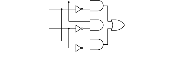
The laws of Boolean algebra can be used to transform Boolean
equations and their corresponding circuits, and to verify equivalence of
Boolean expressions and circuits. However, they don’t provide a recipe
for finding an optimal circuit. That’s mainly because the criteria for opti-
mization depend on many different factors, including the implementation
fabric to be used, power consumption constraints, physical packaging
requirements, design resources available, and others. Optimization proce-
dures, such as use of Karnaugh maps and the Quine-McClusky procedure,
are described in many textbooks on digital logic design. They and other
more involved procedures are founded on the laws of Boolean algebra.
Given the complexity of the Boolean equations in real-world systems and
the fact that computer aided design tools are needed to make optimiza-
tion tractable, we won’t go into the detail of the procedures in this book.
Rather, we will focus on identifying the constraints that apply so that we
can bring appropriate tools to bear on design problems.
2.1.3 VERILOG MODELS OF BOOLEAN EQUATIONS
In the design methodology described in Chapter 1, we focused on the
use of models expressed in an HDL such as Verilog. Modern CAD tools
are very good at analyzing, verifying and synthesizing Boolean functions
expressed in an HDL. In this section, we will see how to express Boolean
equations in Verilog. Later, as we introduce more complex combinational
components and circuits, we will also show how they can be expressed in
Verilog.
As we mentioned earlier, a Boolean equation in which a name is defined
to be equal to a Boolean expression can be implemented by the circuit for
the expression yielding an output with the given name. We can write a
Boolean equation directly in Verilog using an assignment statement within
a module. We use the keyword assign, then write the name of a net or port
on the left hand side of the assignment symbol, “=”, and a Verilog expres-
sion corresponding to the Boolean expression on the right hand side.
2.1 Boolean Functions and Boolean Algebra CHAPTER TWO 51
x
f
y
z
FIGURE 2.11 A circuit that
implements the sum-of-products
form.

52 CHAPTER TWO combinational basics
example 2.6 Develop a Verilog model for a circuit that implements the
Boolean equation of Example 2.5.
solution The equation refers to three inputs, x, y and z, and one output,
f. We represent them as input and output ports in the module definition. The
module contains an assignment statement that represents the Boolean equation,
as follows:
module circuit ( output f,
input x, y, z );
assign f = (x | (y & ~z)) & ~ (y & z);
endmodule
In order to write arbitrary Boolean equations in Verilog, we need to
know how to form Verilog expressions that mean the same as Boolean
expressions. The example above uses the Verilog operators &, |, and ~,
corresponding to the Boolean operators “·”, “” and the overbar nota-
tion, respectively. Verilog also provides the ^ and ~^ operators, corre-
sponding to the XOR and XNOR operations and the XOR and XNOR
gates that we introduced in Section 2.1.1. However, Verilog does not pro-
vide separate operators for the NAND and NOR operations. Instead, we
model those operations using the ~ operator together with & and |. For
example, we would write the NAND of a and b as ~(a & b). The Verilog
operators, the Boolean expressions they represent and the correspond-
ing gates are summarized in Figure 2.12. Note that Verilog makes the
same assumptions about precedence of logical operations that we have
made for Boolean expressions. The ~ operators are evaluated first, then
& operators, and finally | operators. However, we can include parentheses
in Verilog expressions, as we did in the assignment in Example 2.6, to
clarify or force the order of evaluation of operators.
When we write Verilog models for combinational circuits, we should
generally not try to rearrange the Boolean expressions to imply any par-
ticular circuit of gates or other components. Rather, we should express the
Boolean equations in the way that makes them most readily understood,
then let our CAD tools synthesize and optimize a circuit based on
constraints and our chosen implementation fabric. CAD tools can usually
do a much better job at this than we could do manually. Where a CAD
tool requires us to rearrange an expression to enable an optimization, we
should clearly document the change and the reason for it using comments
in the model code.
a & b a · b
a + b
a · b
a + b
a ⊕ b
a ⊕ b
a
a | b
~(a & b)
~(a | b)
a ^ b
a ~^ b
~a
FIGURE 2.12 Verilog opera-
tors and their corresponding
Boolean operations and gates.
example 2.7 Develop a Verilog model for a combinational circuit that
implements the following three Boolean equations, representing part of the con-
trol logic for an air conditioner:
heater_on temp_low · auto_temp manual_heat
cooler_on temp_high · auto_temp manual_cool
fan_on heater_on cooler_on manual_fan
solution The module definition defines the input and output ports and
contains assignment statements for the Boolean equations, as follows:
module aircon ( output heater_on, cooler_on, fan_on,
input temp_low, temp_high, auto_temp,
input manual_heat, manual_cool, manual_fan );
assign heater_on = (temp_low & auto_temp) | manual_heat;
assign cooler_on = (temp_high & auto_temp) | manual_cool;
assign fan_on = heater_on | cooler_on | manual_fan;
endmodule
A straightforward synthesis of a digital circuit from this model is shown at
the top of Figure 2.13. There are two subcircuits, one each for
heater_on and
cooler_on. The outputs of these circuits then drive the third subcircuit for
fan_on. For some implementation fabrics, however, CAD tools might transform
the circuit as shown at the bottom of Figure 2.13. The logical OR operations
2.1 Boolean Functions and Boolean Algebra CHAPTER TWO 53
temp_low
temp_high
auto_temp
manual_heat
manual_cool
manual_fan
cooler_on
heater_on
fan_on
temp_low
temp_high
auto_temp
manual_heat
manual_cool
manual_fan
cooler_on
heater_on
fan_on
FIGURE 2.13 Circuits
corresponding to the assignment
statements for the air conditioner
control logic.

54 CHAPTER TWO combinational basics
that produce the heater_on and cooler_on outputs are replicated and merged
with the logical OR operation for
fan_on. This circuit would fit well in a sum-
of-products implementation fabric, and would have reduced propagation delay
in that fabric.
1. Write a truth table for the Boolean function f a
_
b
_
c.
2. Use truth tables to show that the Boolean expression
__
ab is
equivalent to
_
a
_
b.
3. What is meant by a Boolean expression being in sum-of-products form?
4. Write the truth table for the AND-OR-invert gate shown in
Figure 2.3.
5. Why are buffers used in digital circuits?
6. Use the “don’t care” notation for inputs to compact the truth table
for the function f
1
shown in Table 2.4.
7. What is the benefi t of using the “don’t care” notation for outputs in
a truth table?
8. What is the dual of the following Boolean equation?
____
a b c
_
a
_
b
_
a
_
c
9. Write a Verilog assignment statement to model the Boolean equation
fa
_
b
_
c.
10. Why should we generally not try to optimize Boolean equations
manually when modeling them in Verilog?
2.2 BINARY CODING
Thus far, we have looked at digital representation of information that has
two possible values and shown how we can use Boolean algebra as the
formal basis for circuits that deal with such information. We now extend
our discussion to dealing with information involving more than two val-
ues. An obvious example is numeric information. However, since repre-
sentation and computation of numeric information is such an important
and extensive topic, it deserves a chapter of its own (Chapter 3). First, we
will look at more general principles that underlie digital representation of
all forms of information.
We saw in Chapter 1 that we can represent two-valued information
with two distinct voltage levels in a circuit. Using our digital abstraction,
we called the levels “low” and “high,” but then refined them to ranges
KNOWLEDGE
TEST QUIZ
KNOWLEDGE
TEST QUIZ

of voltages for pragmatic reasons. If we need to represent information
that can take on N possible values, we could choose N distinct voltage
levels (or voltage ranges, with intermediate thresholds). However, design-
ing electronic circuits that can distinguish between more than two levels
is extremely complex, and we would lose many of the benefits of binary
digital circuits.
A better approach is to use multiple binary signals to represent
a multivalued piece of information. Since each individual signal is
binary, we can continue to use binary logic gates in our circuits with
all of the advantages that they afford. We will use the values 0 and 1,
as we did when discussing Boolean algebra, as the abstract values for
each binary signal. We will continue to use the term bit to refer to these
values.
Suppose that we have two signals, a
1
and a
0
, available for represent-
ing some information. There are four possible combinations of binary
values for the pair (a
1
, a
0
), namely, (0, 0), (0, 1), (1, 0) and (1, 1). Each
possible combination is called a code word, and the set of all of the code
words is called a binary code. Since a two-bit code has four possible
code words, we can use a two-bit code to represent information with any
number of values up to and including four. We just need to specify which
code word corresponds to which value of the information. We say that
a code word encodes the corresponding value.
example 2.8 Devise a binary code for the state of a road traffi c light.
The possible states are red, yellow and green.
solution Since there are three possible values to represent, we can use
a two-bit binary code with one code word unused. One possible code is
red: (0, 0) yellow: (0, 1) green: (1, 0)
In this case, the code word (1, 1) is unused.
If two bits, with four possible code words, are not sufficient for the
information we need to represent, we can just use more bits. In general
an n-bit code has 2
n
possible code words, so an n-bit code can represent
information with up to 2
n
values. Conversely, if we need to represent
information with N values, we need at least ⎡log
2
N⎤ bits in our code. (The
notation
⎡x⎤ is called ceiling of x, and denotes the smallest integer that is
greater than or equal to x.) We might choose a longer code, for a variety
of reasons that we will explore, in which case there will be more unused
code words.
2.2 Binary Coding CHAPTER TWO 55

56 CHAPTER TWO combinational basics
example 2.9 Many ink-jet printers have six cartridges for different
colored ink: black, cyan, magenta, yellow, light cyan and light magenta. A multi-
bit signal in such a printer indicates selection of one of the colors. Devise a
minimal length code for the signal.
solution Since there are six values to encode, the minimal length code
is ⎡log
2
6⎤ 3 bits long. There are 2
3
8 possible code words, so two will remain
unused. One possible code is
black: (0, 0, 1) cyan: (0, 1, 0) magenta: (0, 1, 1)
yellow: (1, 0, 0) light cyan: (1, 0, 1) light magenta: (1, 1, 0)
While it might make sense in some cases to use the shortest code, in
other cases a longer code is better. A particular case of a non–minimal-
length code is a one-hot code, in which the code length is the number
of values to be encoded. Each code word has exactly one 1 bit with the
remaining bits 0. The advantage of a one-hot code becomes clear when
we want to test whether the encoded multibit signal represents a given
value; we just test the single-bit signal corresponding to the 1 bit in the
code word for that value.
example 2.10 Devise a one-hot code for the state of the traffi c light
described in a preceding example.
solution Since there are three values to encode, we need a 3-bit one-hot
code. A possible code is
red: (1, 0, 0) yellow: (0, 1, 0) green: (0, 0, 1)
With this code, the left-most bit can be used to activate the red light, the middle
bit to activate the yellow light, and the right-most bit to activate the green light.
No additional circuitry is needed to decode the encoded signals to determine
which light to activate.
2.2.1 USING VECTORS FOR BINARY CODES
Since a collection of binary coded bits conceptually represents a single
piece of information, it would be convenient to be able to represent it as
a single net in Verilog. We can do so using a vector net instead of using
several individual nets. For example, if we need a net w to carry a 5-bit
binary coded value, we could declare it as
wire [4:0] w;

This defines w to be a collection of five nets, w[4], w[3], w[2], w[1] and
w[0], each of which is a single bit. Apart from condensing the declaration
of the nets quite considerably, using vectors for encoded values gives us
many other benefits, as we shall see throughout this book.
When we declare a vector net or port, the part in brackets (4:0 in the
above example) specifies the index range for the elements of the vector.
The first value is the index of the left-most element, and the second value
is the index of the right-most element. If we want to number elements in
descending order, we make the left-most index greater than the right-most
index, as in the above example. We can also number elements in ascend-
ing order by making the left-most index less than the right-most index, as
in the following:
wire [1:3] a;
Here, the elements from left to right are w[1], w[2] and w[3]. The choice
between ascending and descending order is often a question of style, and
may be addressed by coding guidelines used in an organization. This
example also shows that we don’t have to use 0 for the least index value;
it can be any number.
example 2.11 Assume that the one-hot code for the traffi c lights in
Example 2.10 is represented using a 3-element vector with element 1
corresponding to red, 2 to yellow and 3 to green. Develop a Verilog model for a
light controller that has an encoded input, an encoded output, and a single-bit
input that enables the lights. When the enable input is 1, the encoded output is
the same as the encoded input. When the enable input is 0, all bits of the output
are 0.
solution One approach is to control each bit of the output by “AND-
ing” the corresponding input with the enable bit. A module that does this is
module light_controller_and_enable
( output [1:3] lights_out,
input [1:3] lights_in,
input enable );
assign lights_out[1] = lights_in[1] & enable;
assign lights_out[2] = lights_in[2] & enable;
assign lights_out[3] = lights_in[3] & enable;
endmodule
2.2 Binary Coding
CHAPTER TWO 57

58 CHAPTER TWO combinational basics
An alternative approach is to use the enable input to select whether to assign the
input to the output (when enable is 1) or to set the output to all 0 bits otherwise.
A module that takes this approach is
module light_controller_conditional_enable
( output [1:3] lights_out,
input [1:3] lights_in,
input enable );
assign lights_out = enable ? lights_in : 3'b000;
endmodule
The assignment statement in this module uses the ? : operator to select between
the alternatives. Note that we use the notation
3'b000 to form a literal vector
value of three 0 bits. The notation '
b specifies that a binary code word follows,
and the number before '
b specifies how many bits in the vector.
2.2.2 BIT ERRORS
While digital circuits are much more immune to noise than analog electrical
circuits, they are not completely immune from interference. The effect of
interference is occasionally to change the value of a signal from 0 to 1 or
from 1 to 0. We sometimes prosaically call this a bit flip. If the signal is a
single bit representing a logical condition, the rest of the circuit continues
operating on the incorrect value, possibly causing erroneous outputs. If
the signal is one of several bits in a binary-coded representation of some
information, there are two possibilities. The flipped bit results in the code
word being changed either to another valid code word or to a bit com-
bination that is not a valid code word. If the result is a valid code word,
the rest of the circuit operates on the incorrect value, as in the single-bit
case, possibly producing erroneous outputs. If the result is an invalid code
word, operation of the circuit depends on how we deal with invalid codes
in the design.
One design approach is to consider invalid code words as “ impossible”
inputs, and not to specify the behavior of circuits that operate on invalid
inputs. If we adopt this approach, the actual behavior of the circuits will
depend on the implementation for the valid-code-word cases and on opti-
mizations performed by CAD tools. It may be acceptable not to care about
the circuit output values for invalid code words, particularly if cost reduc-
tion is a driving constraint. For example, in a mass-produced consumer
toy, no one really cares about a once-a-year glitch, particularly if fixing it
would increase the cost from $1.00 to $1.05.

If, on the other hand, the application demands more deterministic
outputs, we can adopt a “fail safe” design approach. We can design our
circuit to produce correct outputs for valid code words, and to produce
known safe outputs should an invalid code word arise due to interference.
For example, in our ink-jet printer of Example 2.9, if interference caused
the signal for selecting the color to take on the code word (1, 1, 1), we
could deliberately select no color, rather than spoiling a printout with
incorrect colors or damaging the mechanism by trying to select more than
one color at once.
example 2.12 In Example 2.10, we suggested that the bits of the one-
hot-coded signal could be used to activate the red, yellow and green lights,
respectively. However, an error in the three-bit signal could cause multiple lights
to activate, or no light to activate. Design a circuit that causes the three lights
to activate normally for valid one-hot code words, and for the red light to be
activated alone for invalid code words.
solution Let us represent the three-bit signal with the bits s_red, s_yellow
and s_green. The green light should be activated only when s_green is 1 and
s_yellow and s_red are both 0. The Boolean equation is
green
___
s_red ·
____
s_yellow · s_green
Similarly, the yellow light should be activated when s_yellow is 1 and s_green
and s_red are both 0, giving the Boolean equation
yellow
___
s_red · s_yellow ·
____
s_green
The red light should be activated when s_red is 1 and s_yellow and s_green are
both 0, but it should also be activated in all other cases when neither the green
nor yellow light is activated. The Boolean equation is
red s_red ·
____
s_yellow ·
____
s_green
_______
(green yellow)
There are many other ways we could write this last Boolean equation, for
example, by substituting for green and yellow and using the laws of Boolean
algebra to rearrange it. However, we can leave that to a CAD tool, and simply
enter the equations in the form above as part of a Verilog model.
A third design approach to dealing with errors introduced by interfer-
ence is to have the circuit detect when they occur and then to take excep-
tional action. This is, in a sense, an extension of the “fail safe” approach.
However, rather than producing a safe “normal” output, the circuit pro-
duces an “exceptional” output that indicates the circuit’s function has not
been performed correctly. An example of this approach is seen in modern
2.2 Binary Coding CHAPTER TWO 59

60 CHAPTER TWO combinational basics
cars that include digital circuits to manage the engine. If an error arises, the
circuit detects the error and illuminates a warning light in the instrument
panel as its exceptional output. Detecting that interference has flipped
a bit in a code word requires that the code include unused code words,
and that the bit flip change a valid code word to one of the invalid code
words. Circuits that use the encoded information can check for invalid
code words and take action, such as suppressing outputs or activating an
error signal. Of course, if interference causes a valid code word to change
to a different valid code word, the error would not be detected.
One technique that is often used for error detection is parity, which
refers to the number of bits that are 1 in a code word. Parity error check-
ing involves increasing the code length by one bit, called the parity bit. In
the even parity scheme, the parity bit in each augmented code word is set
to 0 or 1 to ensure that the total number of 1 bits is even. For example,
if the original code word is 1011, the augmented code word is 10111.
(The converse odd parity scheme sets the parity bit to ensure that the
total number of 1 bits is odd.) In an even parity scheme, valid augmented
code words have even parity, and invalid augmented code words have
odd parity. If interference causes a 0 bit to change to 1, the number of 1
bits is increased by one, making the parity odd. Similarly, if interference
changes a 1 bit to 0, the number of 1 bits is decreased by one, again mak-
ing the parity odd. So to check whether a bit has flipped, we simply count
the number of 1 bits, including the parity bit. If the count is odd, parity
has been reversed, so an error has occurred. If the count is even, either no
error has occurred, or an even number of bits have been flipped, which
we can’t detect. In many applications, the probability of two or more bits
flipping is much lower than the probability of one bit flipping, so it is
acceptable not to be able to detect an even number of bit flips.
Counting the number of bits in a code word might, at first, seem a
rather complicated function to perform. However, since we’re only inter-
ested in whether the total is even, the task is much simpler. For a code
of original length 2, the function p to generate the parity bit so that the
augmented code has even parity is shown in the truth table in Table 2.8.
As we can see, this function is equivalent to the exclusive-OR function.
So we can use an exclusive-OR gate to generate the parity bit to augment
a 2-bit code. We can extend this to augment a 3-bit code by taking the
exclusive OR of the parity of two bits with the third bit. In general, for
a code of any length, we can just take the exclusive OR of all of the bits.
Since the exclusive-OR function is commutative and associative, the order
in which we apply the exclusive OR to the bits of the code doesn’t matter.
A common approach is to use a parity tree, as shown in Figure 2.14, since
it keeps the overall propagation delay small and avoids using gates with
large numbers of inputs. The tree at the left of the figure generates the
parity bit to augment an 8-bit code, creating a code of nine bits with even
a
1
a
0
p
000
011
101
110
TABLE 2.8 Truth table for
the parity bit of a code of original
length 2, giving even parity for the
augmented code.
2.2 Binary Coding CHAPTER TWO 61
a
0
a
1
a
2
a
3
a
4
a
5
a
6
a
7
a
0
a
1
a
2
a
3
a
4
a
5
a
6
a
7
p
error
p
parity. The tree at the right checks the augmented code and yields a 1 if
there is a parity error.
There are two problems with parity schemes. First, if interference
flips two bits, parity is preserved, so we miss that error. The same applies
if four, six, or any even number of bits are flipped. In many applications,
however, the probability of multiple bits being flipped is extremely low, so
the cost of a more elaborate error detection scheme is not warranted. The
second problem is that for any given invalid code word, there are several
possible bit flips from a valid code word that could yield the invalid code
word. So while we can detect occurrence of a single-bit error, we can’t tell
which bit is in error. If detection of errors and taking some exceptional
action is sufficient for the application, parity is a good choice. However,
if corrective action is needed, the approach can be extended by including
sufficient invalid code words in the code that a flip of any given bit yields
a distinct invalid code word. When that invalid code word is detected,
it indicates that the given bit has been flipped. So correcting the error is
simply a matter of flipping it back, that is, using the negation of that bit’s
value. This kind of code is called an error correcting code (ECC).
The design of codes to provide for error detection and correction is
a very broad topic area. We will return to it as part of our discussion of
storage in Chapter 5, since that is one place where errors can arise. Mean-
while, when we design circuits that operate on binary coded information,
we should think about how they should behave when interference pro-
duces bit errors.
1. How many code words are possible with a code of 5 bits?
2. What is the minimum number of bits needed to encode information
with 12 possible values?
3. Devise a one-hot code to represent the days of the week (Monday
through Sunday).
KNOWLEDGE
TEST QUIZ
KNOWLEDGE
TEST QUIZ
FIGURE 2.14 Parity trees
for generating (left) and checking
(right) even parity.
62 CHAPTER TWO combinational basics
4. Write a Verilog declaration for a net, named w, representing an 8-bit
binary coded value.
5. Write a Verilog assignment that drives each bit of w with a 0 value.
6. Does a single bit fl ip in a one-hot code word produce an invalid
code word always, never, or sometimes?
7. How does extending a code with a parity bit to ensure odd parity
enable detection of single-bit errors?
8. Can parity checking be used to correct the effect of a bit fl ip? If so,
how? If not, why not?
2.3 COMBINATIONAL COMPONENTS
AND CIRCUITS
In this section, we will introduce a number of combinational circuit compo-
nents that are used as building blocks in larger digital systems. While these
components can, themselves, be constructed from gates, it is generally not
useful to do so. Instead, we will work at a higher level of abstraction. We
will think of these components as basic blocks that, together with gates,
are used to construct complex combinational circuits. We will rely on syn-
thesis tools to refine our descriptions of such circuits into implementations
using gates or other elements provided by the target implementation fabric.
We will also return to the notion of negative logic, briefly mentioned in
Chapter 1. The material presented in this section will form the basis for
our consideration of larger-scale digital systems in later chapters.
2.3.1 DECODERS AND ENCODERS
In Section 2.2, we described how information can be binary coded. In
many designs, we need to derive a number of control signals from a binary
coded signal, with one control signal corresponding to each valid code
word. When the encoded signal takes on a given code value, the corre-
sponding control signal is activated. We call a circuit that derives the con-
trol signals in this way a decoder. For an n-bit code, if every code word
is valid, the decoder will have 2
n
outputs. As we shall see in Chapter 5,
decoders are an important building block in memory designs.
We can derive the Boolean equation for each output of a decoder by
looking at the corresponding code word. To illustrate, suppose we have
an encoded 4-bit input signal (a
3
, a
2
, a
1
, a
0
), and we need to determine the
Boolean equation for the output corresponding to the code word 1011.
The output is 1 only when a
3
1, a
2
0, a
1
1 and a
0
1. Thus, the
output is the value of the expression

a
3
·
_
a
2
· a
1
· a
0
A similar argument applies for other outputs. Each is the logical AND of
the input bits, either directly (for bits that are 1 in the corresponding code
word) or negated (for bits that are 1 in the corresponding code word).
example 2.13 Develop a Verilog model for a decoder for use in the ink-
jet printer described in Example 2.9. The decoder has three input bits represent-
ing the choice of color cartridge and six output bits, one to select each cartridge.
solution A module with assignment statements representing the Boolean
equations for the outputs is
module ink_jet_decoder ( output black, cyan, magenta, yellow,
light_cyan, light_magenta,
input color2, color1, color0 );
assign black = ~color2 & ~color1 & color0;
assign cyan = ~color2 & color1 & ~color0;
assign magenta = ~color2 & color1 & color0;
assign yellow = color2 & ~color1 & ~color0;
assign light_cyan = color2 & ~color1 & color0;
assign light_magenta = color2 & color1 & ~color0;
endmodule
If an invalid code occurs on the input bits, none of the outputs is activated. This
can be considered a “fail safe” design.
The inverse of a decoder is called an encoder. It has, as inputs, a num-
ber of single-bit signals, and as outputs, a collection of signals representing
the bits of an encoded value. We will assume for the moment that at most
one of the inputs is 1 at any time, and the others are all 0. The code word
at the output corresponds to the particular input that is 1.
We can derive the Boolean equation for each bit of the output by
identifying those inputs for which the output bit is 1. The output bit is
then the logical OR of those inputs. However, we need to take account
of the possibility that none of the inputs is 1, since that would cause our
encoder to output a code word of all 0 bits. If that code word is invalid,
we can use it to imply that no inputs are 1, essentially extending the code.
Alternatively, if the all-0s code word is valid and corresponds to one of
the inputs being 1, we need to have a separate output that indicates when
any of the inputs is 1. When this output is 0, we ignore the code word
produced by the encoder.
2.3 Combinational Components and Circuits CHAPTER TWO 63

64 CHAPTER TWO combinational basics
example 2.14 Design an encoder for use in a domestic burglar alarm that
has sensors for each of eight zones. Each sensor signal is 1 when an intrusion
is detected in that zone, and 0 otherwise. The encoder has three bits of output,
encoding the zone as follows:
Zone 1: 000 Zone 2: 001 Zone 3: 010 Zone 4: 011
Zone 5: 100 Zone 6: 101 Zone 7: 110 Zone 8: 111
solution Since all code words are used, we need a separate output to
indicate when there is a valid code-word output. The module definition is
module alarm_eqn ( output [2:0] intruder_zone,
output valid,
input [1:8] zone );
assign intruder_zone[2] = zone[5] | zone[6] |
zone[7] | zone[8];
assign intruder_zone[1] = zone[3] | zone[4] |
zone[7] | zone[8];
assign intruder_zone[0] = zone[2] | zone[4] |
zone[6] | zone[8];
assign valid = zone[1] | zone[2] | zone[3] | zone[4] |
zone[5] | zone[6] | zone[7] | zone[8];
endmodule
The left-most bit of the output code is 1 when any of the zone 5 through zone
8 inputs is 1, so the equation for that output is the logical OR of those zone
inputs. The equations for the other two output code bits are derived similarly.
The
valid output is the logical OR of all of the zone inputs.
Now let’s consider the possibility of more than one input to an encoder
being 1 at a time. The design we described above would produce an incor-
rect output, possibly an invalid code word. The solution is to assign pri-
orities to the inputs, so that if multiple inputs are 1, the encoder outputs
the code word corresponding to the input with highest priority. Such an
encoder is called, not surprisingly, a priority encoder. One application
of priority encoders is to prioritize interrupts in embedded systems. (We
describe interrupts in Chapter 8.)
example 2.15 Revise the encoder for the burglar alarm to be a priority
encoder, with zone 1 having highest priority, down to zone 8 having lowest priority.
solution The port list is unchanged, since we need the same inputs and
outputs for the encoder. The truth table for the priority encoder is shown in

Table 2.9. From this, we can derive the Boolean equations for each bit of the
output. A revised module definition is shown below.
module alarm_priority ( output [2:0] intruder_zone,
output valid,
input [1:8] zone );
wire [1:8] winner;
assign winner[1] = zone[1];
assign winner[2] = zone[2] & ~zone[1];
assign winner[3] = zone[3] & ~(zone[2] | zone[1]);
assign winner[4] = zone[4] & ~(zone[3] | zone[2] | zone[1]);
assign winner[5] = zone[5] & ~( zone[4] | zone[3] | zone[2] |
zone[1]);
assign winner[6] = zone[6] & ~( zone[5] | zone[4] | zone[3] |
zone[2] | zone[1]);
assign winner[7] = zone[7] & ~( zone[6] | zone[5] | zone[4] |
zone[3] | zone[2] | zone[1]);
assign winner[8] = zone[8] & ~( zone[7] | zone[6] | zone[5] |
zone[4] | zone[3] | zone[2] |
zone[1]);
assign intruder_zone[2] = winner[5] | winner[6] |
winner[7] | winner[8];
assign intruder_zone[1] = winner[3] | winner[4] |
winner[7] | winner[8];
assign intruder_zone[0] = winner[2] | winner[4] |
winner[6] | winner[8];
assign valid = zone[1] | zone[2] | zone[3] | zone[4] |
zone[5] | zone[6] | zone[7] | zone[8];
endmodule
2.3 Combinational Components and Circuits
CHAPTER TWO 65
zone intruder_zone
(1) (2) (3) (4) (5) (6) (7) (8) (2) (1) (0) valid
1–––––––000 1
01––––––001 1
001–––––010 1
0001––––011 1
00001–––100 1
000001––101 1
0000001–110 1
00000001111 1
00000000––– 0
TABLE 2.9 Truth table for a
priority encoder for a burglar alarm.

66 CHAPTER TWO combinational basics
In this module, each element of the internal net winner indicates when the cor-
responding zone is 1 and has not lost to a higher priority zone. The encoder
then uses the elements of the internal net instead of the zone inputs directly to
generate the output code word. Another way of expressing this in Verilog is
shown in the following module:
module alarm_priority_1 ( output [2:0] intruder_zone,
output valid,
input [1:8] zone );
assign intruder_zone = zone[1] ? 3'b000 :
zone[2] ? 3'b001 :
zone[3] ? 3'b010 :
zone[4] ? 3'b011 :
zone[5] ? 3'b100 :
zone[6] ? 3'b101 :
zone[7] ? 3'b110 :
zone[8] ? 3'b111 :
3'b000;
assign valid = zone[1] | zone[2] | zone[3] | zone[4] |
zone[5] | zone[6] | zone[7] | zone[8];
endmodule
The conditional assignment in this module tests a series of conditions to
determine the value to assign to the net
intruder_zone. First the zone 1 input is
tested, and the result assigned 000 if the zone 1 input is 1. Otherwise, the zone
2 input is tested, and the result assigned 001 if the zone 2 input is 1. Testing con-
tinues in this way, with priority implied by the order of testing the conditions.
This form of assignment for priority encoding is much easier to understand, and
leaves the hard work of determining and optimizing the Boolean equations to
the synthesis CAD tool.
BCD Code and 7-Segment Decoders
One form of information that we might wish to encode is numeric infor-
mation. As we mentioned earlier, we will look at this topic in detail in
Chapter 3. However, in this section, we will look at a particular form of
numeric coding called binary coded decimal (BCD). If we consider just a
single decimal digit, the ten possible values are 0, 1, 2, 3, 4, 5, 6, 7, 8 and
9. We need at least 4 bits in a binary code for these values. There are a
large number of possible codes, but BCD is the most common, having the
following code words:
0: 0000 1: 0001 2: 0010 3: 0011 4: 0100
5: 0101 6: 0110 7: 0111 8: 1000 9: 1001
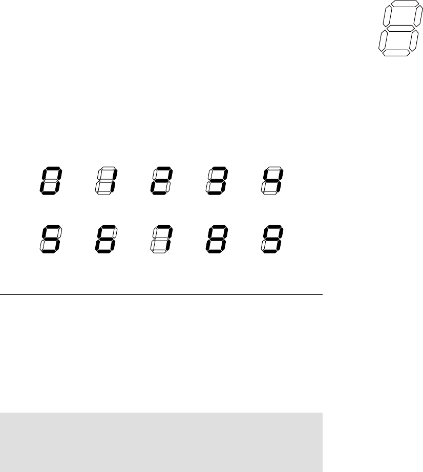
If we have more than one decimal digit of information to represent, we
simply use groups of four bits, with each group corresponding to one decimal
digit. For example, a system that deals with three-digit numbers would use
a 12-bit code. The number 493 would be encoded as 0100 1001 0011.
Many digital systems display decimal numbers using 7-segment dis-
plays. Each display digit consists of seven separate lights, arranged as
shown in Figure 2.15. If we have a digit encoded using BCD and we need
to display the digit on a 7-segment display, we need a 7-segment decoder.
Strictly speaking, we should call it a “7-segment code converter,” since it
converts from a BCD code input to a 7-segment code output. However,
the term “7-segment decoder” is widely used. Assuming a segment is lit if
its input is 1, we need a 7-bit code for representing the digits 0 through 9.
The code word for each digit has a 1 bit corresponding to each seg-
ment that is lit and a 0 bit corresponding to each segment that is not lit.
A 7-segment decoder then converts between BCD and this 7-bit code. One
possible code is shown in Figure 2.16, with the bits corresponding left to
right with segments g through a.
2.3 Combinational Components and Circuits CHAPTER TWO 67
a
b
c
d
e
f
g
FIGURE 2.15 A 7-segment
display digit. The segments are
named “a” through “g,” as shown.
0111111 0000110 1011011 1001111 1100110
1101101 1111101 0000111 1111111 1101111
FIGURE 2.16 A 7-segment
code for decimal digits. In each
code word, the bits correspond to
segments g through a in left-to-
right order.
example 2.16 Develop a Verilog model for a 7-segment decoder. Include
an additional input,
blank, that overrides the BCD input and causes all segments
not to be lit.
solution We could determine the BCD code words that result in each
segment being lit, and so derive Boolean equations for each segment output.
However, that would make the model hard to understand. A better approach is
to list the 7-bit code word corresponding to each BCD code word, as we did in
Figure 2.16. A module that does this is
module seven_seg_decoder ( output [7:1] seg,
input [3:0] bcd,
input blank );
reg [7:1] seg_tmp;
(continued)

68 CHAPTER TWO combinational basics
always @*
case (bcd)
4'b0000: seg_tmp = 7'b0111111; // 0
4'b0001: seg_tmp = 7'b0000110; // 1
4'b0010: seg_tmp = 7'b1011011; // 2
4'b0011: seg_tmp = 7'b1001111; // 3
4'b0100: seg_tmp = 7'b1100110; // 4
4'b0101: seg_tmp = 7'b1101101; // 5
4'b0110: seg_tmp = 7'b1111101; // 6
4'b0111: seg_tmp = 7'b0000111; // 7
4'b1000: seg_tmp = 7'b1111111; // 8
4'b1001: seg_tmp = 7'b1101111; // 9
default: seg_tmp = 7'b1000000; // "-" for invalid code
endcase
assign seg blank ? 7’b0000000 : seg_tmp;
endmodule
We have written the list of code-word values in a case statement contained
within an always block. (An always block is one kind of procedural block; we
shall return to the other kind in Section 2.4). For a combinational function, the
always block starts with an event list of the form
@*, indicating that the block
responds to any change of value on any of the inputs to the function. The case
statement includes an expression in parentheses whose value is used to select
among the alternatives. Each alternative lists a possible value of the expres-
sion (before the
: character) and has an assignment to seg_tmp. The default
alternative in the case statement deals with values not explicitly listed. In this
module, the default alternative deals with invalid codes. Note that Verilog
requires the target of an assignment within a procedural block to be declared
as a variable, in this case using the keyword
reg, instead of as a net using the
keyword
wire. The difference is that a variable retains the value assigned within
a block, whereas a net continuously gains its value from an assignment state-
ment (written outside a block using the assign keyword) or from a connection
to an instance. The final assignment statement within the module uses the
blank input to determine whether to drive the encoded output with all 0s, caus-
ing all segments not to be lit, or to copy the value decoded from the BCD input
to the output.
2.3.2 MULTIPLEXERS
Multiplexers are an important building block in many digital systems. We
introduced a simple multiplexer in Section 1.2. It has two data inputs, one
data output, and a select input that determines which input value is used
for the output value. We can expand on this simple multiplexer along two
dimensions. First, we can add more data inputs, which also requires adding

further select inputs to encode the choice of input to drive the output.
Second, we can use multiplexers in parallel to select between two sources
of multibit encoded data. Let’s look at the alternatives in more detail.
Suppose that, instead of selecting between two input bits, we need to
select between four input bits. Since there are four input sources, we need
to have four values for the select input. We can encode the select input
using two bits. Figure 2.17 shows a 4-to-1 multiplexer. The select input is
drawn as a thicker line to indicate that it is a multibit encoded input. In
this book, we will mostly use line thickness to distinguish between single-
bit and multibit signals. Occasionally, where we want to emphasis that a
signal is multibit, we will add a stroke across the line and show the num-
ber of bits, as in Figure 2.17. The code for the select input is
00: input 0 01: input1 10: input 2 11: input 3
We could describe a gate circuit to implement the multiplexer, but
there is little point, for two reasons. First, a synthesis tool would probably
optimize the circuit, changing it from what we specify. Second, in a num-
ber of implementation fabrics, multiplexers can be constructed from indi-
vidual transistors more efficiently than as a circuit of gates. Multiplexers
would be considered primitive elements in those fabrics. So instead of
a gate-level circuit, we will just consider how to express a multiplexer
function in Verilog.
example 2.17 Develop a Verilog model for a 4-to-1 multiplexer.
solution The module definition is
module multiplexer_4_to_1 ( output reg z,
input [3:0] a,
input sel );
always @*
case (sel)
2'b00: z a[0];
2'b01: z a[1];
2'b10: z a[2];
2'b11: z a[3];
endcase
endmodule
The case statement in the always block uses the value of the sel input to deter-
mine which input bit to copy to the output. This example illustrates a further
point about using always blocks to model combinational functions. As we
2.3 Combinational Components and Circuits CHAPTER TWO 69
0
1
2
3
2
FIGURE 2.17 A 4-to-1
multiplexer.
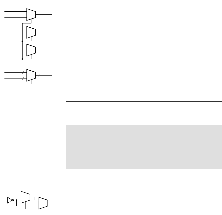
70 CHAPTER TWO combinational basics
mentioned in Example 2.16, the target of the assignments in the block must be
declared as a variable, using the keyword
reg in this case. When the target is a
port of the module, the
reg declaration can be combined with the output port
declaration.
We can further expand this multiplexer to have eight data inputs,
which would require a 3-bit select input. The number of data inputs need
not be a power of 2. If it is not, then the select input code will have unused
code words. We must then ensure that an invalid code word is never pre-
sented to the select input. In general, a multiplexer having N input bits
needs ⎡log
2
N⎤ bits for the select input, since the select input carries a
binary code requiring N values.
Now let’s consider using multiplexers to select between two sources
of encoded data. If the code length is m (that is, each code word has
m bits), we can use m two-input multiplexers, one for each bit of the two
data sources. This is illustrated in Figure 2.18 for selecting between two
sources each of three bits. The circuit at the top of the figure shows the
three separate 2-to-1 multiplexers. At the bottom of the figure is a symbol
that represents a 2-to-1 multiplexer operating on the 3-bit encoded data
inputs and output.
example 2.18
Develop a Verilog model for the 3-bit 2-to-1 multiplexer.
solution The module definition is
module multiplexer_3bit_2_to_1 ( output [2:0] z,
input [2:0] a0, a1,
input sel );
assign z = sel ? a1 : a0;
endmodule
We can, of course, combine these two forms of expansion. If we need
to select between N sources of data, each of which is encoded with m bits,
we simply use m lots of N-to-1 multiplexers. The details are left as an
exercise.
Before we leave the topic of multiplexers, it is interesting to note that
all Boolean functions can be expressed in terms of multiplexers combined
with negation. To illustrate, consider the function that we examined ear-
lier, f ( x y)
_
z whose truth table is shown in Table 2.2. This function
can be implemented using the circuit shown in Figure 2.19. Note the use
of a literal 0 value for one input. This can be implemented by hard wiring
0
1
0
1
0
1
0
1
a0(0)
a1(0)
z(0)
a0
3
3
3
a1
z
a0(1)
a1(1)
z(1)
a0(2)
a1(2)
sel
sel
z(2)
FIGURE 2.18 A circuit for
a 2-to-1 multiplexer for 3-bit data
sources (top), and a symbol for the
multiplexer (bottom).
f
z
y
x
0
0
1
0
1
FIGURE 2.19 Implementing
a Boolean function using
multiplexers.

the input to the 0V ground. We won’t go into the general principles of
how to implement Boolean functions using multiplexers here. We raise
the topic since multiplexers can be very efficiently implemented in some
fabrics. As an example, the basic circuit elements in FPGAs manufac-
tured by Actel Corporation consist of two multiplexers and a small num-
ber of other associated components. However, the details of mapping
arbitrary Boolean equations to multiplexers are generally handled by
CAD tools.
2.3.3 ACTIVE-LOW LOGIC
Thus far, we have focused on circuits in which a low logic level represents
the falsehood of some condition and a high logic level represents truth
of the condition. In Chapter 1, we identified this convention as positive
logic, or active-high logic. In principle, the correspondence of low with
falsehood and high with truth is largely arbitrary. We could just as well
represent falsehood with a high logic level and truth with a low logic
level, a convention that we referred to in Chapter 1 as negative logic,
or active-low logic. Note that “positive” and “negative” in this context
don’t refer to the voltage polarity, but simply distinguish between the two
conventions. We will use the terms “active high” and “active low” to
avoid the confusion. We will also maintain the convention of associating
0 with a low logic level and 1 with a high logic level.
In a circuit that mixes both active-low and active-high logic, we could
get confused about which convention is used for which signal. We should
still label signals with the conditions they represent so that we can under-
stand the intended function of the circuit. A commonly adopted approach
is to label an active-low signal with the negation of the condition it rep-
resents. For example, an active-low signal representing the condition that
a lamp is lit would be labeled
____
lamp_lit, since the signal is 1 when the con-
dition is false and 0 when the condition is true.
One reason for using active-low logic is that some kinds of digital
circuits are able to sink more current when driving an output low than
they can source when driving the output high. If such an output is used
to activate some condition for which current flow is required, it would be
better to use a low logic level rather than a high logic level.
example 2.19 Revise the night-light circuit from Figure 1.3 in Chapter 1
by connecting the lamp to the positive power supply instead of to ground.
solution To make current flow in the lamp and light it, we need to drive
the controlling signal low. Thus, we must use an active-low signal to implement
the “lamp lit” condition. This is shown in Figure 2.20, in which the controlling
signal is labeled
____
lamp_lit . The gate performs the logical AND function of the
lamp_enabled and dark signals, but its output must be negated to match the
2.3 Combinational Components and Circuits CHAPTER TWO 71
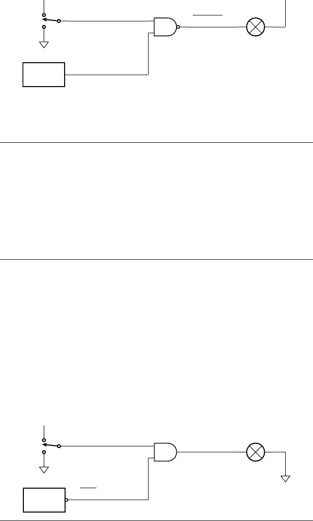
72 CHAPTER TWO combinational basics
FIGURE 2.20 The night-light
circuit using an active-low signal.
lamp_enabled
dark
lamp_lit
sensor
+V +V
negation of the “lamp lit” condition. Hence, we use a NAND gate in place of
the AND gate in the original circuit.
In general, this approach to dealing with active-low logic involves
matching negation “bubbles” on components with active-low signals.
When we do that, no negation of the logical condition represented by
the signal is implied. Thus, we can interpret the circuit of Figure 2.20
as saying, “The lamp is lit when the lamp is enabled and it is dark.” If
we connect an active-low signal to a component without a bubble at the
connection point, we are implying negation of the logical condition rep-
resented by the symbol.
example 2.20
Returning to the original night-light circuit from
Figure 1.3 in Chapter 1, think of the sensor as having an active-low output
representing the condition “it is light.” Redraw the circuit to take account of
this change.
solution As shown in Figure 2.21, we label the signal connected to
the sensor
__
light to show that it is active-low. We draw a bubble on the sensor
output to indicate it is an active-low output. There is no negation implied by
the connection at the sensor output, since we have a bubble output connected to
an active-low signal. However, since there is no bubble on the AND gate input,
logical negation is implied for its connection to
__
light . Thus, we can interpret the
circuit as saying, “The lamp is lit when the lamp is enabled and it is not light.”
lamp_enabled
light
lamp_lit
sensor
+V
FIGURE 2.21 The night-light
circuit with negation implied by
connecting an active-low signal to
an active-high input.
When we draw gate circuits for Boolean functions, it is important to
use AND and OR gates as appropriate for the logical operations applied
to conditions represented by signals. If any of those signals are active-
low, and no implicit negation is intended, we should “draw a bubble”
where the signal connects to a gate. We can make use of DeMorgan’s
laws to derive alternate views of gates. For example, Equation 2.18 tells
us that the component that we have called a NAND gate when operating
on active-high inputs can also perform an OR function upon conditions
represented by active-low inputs. We can draw two distinct symbols for
the gate component, as shown in Figure 2.22. It is important to realize,
however, that both symbols represent the same circuit of interconnected
transistors!
One of the problems we encounter when modeling designs with
active-low signals in Verilog is that we don’t have a way of drawing a
negation bar over a signal name or drawing a bubble on a port. Instead,
we usually adopt a textual naming convention, such as appending the
suffix "_N" to a name, to indicate which signals and ports are active-low.
For example, a Verilog model might give the active-low output of the
sensor in Figure 2.21 the name light_N. A Verilog model for the sensor
would assign 0 to the light_N signal when it is light and 1 when it is dark.
The model for the AND gate assigns 1 to its output when both inputs are
1, and 0 to its output otherwise. Thus, the lamp_lit signal is assigned 1
when lamp_enabled is 1 (“the lamp is enabled”) and light_N is 1 (“it is
not light”). When we’re dealing with active-low logic in Verilog models,
we need to think carefully about which Verilog value represents truth or
falsehood of each condition, and design accordingly.
1. For a decoder with inputs (a
2
, a
1
, a
0
), write the Boolean equation
for the output corresponding to the code word 100.
2. What would be the output of the encoder in Example 2.14 if both
the Zone 2 and Zone 3 inputs were 1 at the same time? Would this
output be correct?
3. What problem would arise if we did not include the valid output
from the encoder in Example 2.14?
4. How does a priority encoder solve the problem of multiple inputs
being 1 at the same time?
5. What decimal digit is represented by the BCD code 0101?
6. What is the 7-segment code corresponding to the BCD code 0011?
7. What is the purpose of a multiplexer?
8. How many select input bits are needed for a 6-to-1 multiplexer?
KNOWLEDGE
TEST QUIZ
KNOWLEDGE
TEST QUIZ
2.3 Combinational Components and Circuits CHAPTER TWO 73
FIGURE 2.22 Alternate logic
symbols for a gate.
74 CHAPTER TWO combinational basics
9. How can we construct a 2-to-1 multiplexer for 5-bit encoded data
inputs?
10. What logic level would you expect on a signal labeled
______
door_closed,
connected to a door sensor, when the door is open?
11. If a Verilog net named motor_on_N represents an active-low
signal, what Verilog value would you assign it to turn the motor on?
2.4 VERIFICATION OF COMBINATIONAL
CIRCUITS
In Section 1.5 we introduced a design methodology to guide us in the
design and implementation of a digital system. The first task was to
develop and enter a design description based on the application’s require-
ments and constraints. In this chapter, we have seen examples of design
descriptions, expressed as schematics and as Verilog models, for simple
combinational circuits and components. Most systems are more involved
and include sequential components as well as combinational subcircuits,
so there is a limit to how much of the methodology we can demonstrate.
Nonetheless, there are small-scale applications where combinational cir-
cuits are sufficient, so we will show how we can apply our design meth-
odology to them.
The second step in our design methodology is functional verification,
that is, ensuring that the design performs the operation required of it.
Since, in a combinational circuit, the values of the outputs depend only
on the current values of the inputs, we can simply verify that the circuit
produces the required output for each combination of input values. For a
design description expressed in Verilog, we can develop a testbench model
that provides input values to the design under verification (DUV) and
checks that the output values are correct. The DUV is also frequently
called a device under test (DUT), but that usage may be confused with
physical testing of manufactured devices. We will use the term DUV in
this book to avoid the confusion. The testbench model is, itself, a Verilog
model that we can execute using a simulator. However, it is not intended
to describe hardware that will be built. Rather, its purpose is to apply a
sequence of values, called test cases, to the input connections of the DUV,
and to monitor the output connections to ensure that correct values are
produced. The DUV is usually an instance of the Verilog module that
describes the design. A simulator mimics the passage of time, executing
the DUV and testbench models, and assigning values to nets and variables
at appropriate simulated times.
The difficult part of developing a testbench model is working out how
to express the correctness conditions. If the requirements are expressed as
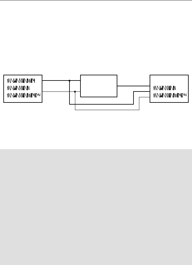
Boolean equations, the design will probably implement those equations
directly, so expressing the correctness conditions as Boolean equations
gains nothing. A better approach is to determine some more abstract con-
ditions that are required to hold, and to test that the design satisfies those
conditions.
example 2.21 Develop a testbench model for the light_controller_and_enable
module for the traffi c light control circuit of Example 2.11. Verify the conditions
that, when the enable input is 1, the output is the same as the light input, and
when the enable input is 0, all light outputs are inactive.
solution The testbench model includes an instance of the design under
verification, as well as code to apply test cases and to check for correct outputs.
The organization of these components is shown in Figure 2.23.
DUV
light_controller
apply_test_cases
lights_in
enable
lights_out
check_outputs
FIGURE 2.23 Organization
of the testbench for the light
controller.
2.4 Verification of Combinational Circuits
CHAPTER TWO 75
Since the testbench is a Verilog model, it needs a modue definition. How ever,
since there are no external connections to the testbench, the module has no
ports. The module definition is
`timescale 1ms/1ms
module light_testbench;
wire [1:3] lights_out;
reg [1:3] lights_in;
reg enable;
light_controller_and_enable duv ( .lights_out(lights_out),
.lights_in(lights_in),
.enable(enable) );
initial begin
enable = 0; lights_in = 3'b000;
#1000 enable = 0; lights_in = 3'b001;
#1000 enable = 0; lights_in = 3'b010;
(continued)

76 CHAPTER TWO combinational basics
#1000 enable = 0; lights_in = 3'b100;
#1000 enable = 1; lights_in = 3'b001;
#1000 enable = 1; lights_in = 3'b010;
#1000 enable = 1; lights_in = 3'b100;
#1000 enable = 1; lights_in = 3'b000;
#1000 enable = 1; lights_in = 3'b111;
#1000 $finish;
end
always @(enable or lights_in) begin
#10
if (!( ( enable && lights_out == lights_in) ||
(!enable && lights_out == 3’b000) ))
$display(“Error in light controller output”);
end
endmodule
The first line is a time-scale directive that indicates to the simulator the time
units to be used for delays in the model. In Verilog models, delays are specified
as numbers without units. The timescale directive is required to ascribe units
to these numbers. In our example, we specify that delays are multiples of 1ms
(the first number in the directive), with a precision of 1ms.
Within the module,
duv is an instantiation of the light_controller_and_enable
module that describes the traffic light control circuit. The input and output ports
of the instance are connected to internal variables and nets declared within the
testbench module. Note that we have used named port connection here, rather
than positional port connection as we did in Example 1.5. In named associa-
tion, we write the name of the module port after the “
.” symbol and the variable
or net to which it is connected within parentheses. This allows us to write the
connections in any order, rather than following the order of ports in the module.
Given the advantages and clarity of named connection, we will use it in models
from now on.
Following the instantiation statement is an initial block that applies test cases to
the DUV. An initial block is the second kind of procedural block, along with the
always block that we introduced in Section 2.3. In general, a procedural block
is a collection of Verilog statements that are executed one after another, much
like statements in a programming language. An initial block starts executing at
the beginni
ng of simulation, and when the last statement in the block has been
executed, it terminates. We only use initial blocks in testbench models, not in
models for circuit designs. In particular, we don’t use initial blocks to set the ini-
tial conditions for sequential circuits. We will see how to reset sequential circuits
in Chapter 4.
The first line of the initial block in this module makes an assignment to the
enable input, followed by an assignment to the lights_in input. These two assign-

ments constitute application of one test case to the inputs of the DUV. The block
then delays, indicated by the
# symbol, for 1000 units of simulated time. Since
the timescale directive specified 1ms as the time unit, the delay is for 1 second
of simulated time. During this delay, other parts of the model, including the
instance of the lights controller, continue executing. After the 1 second delay, the
block continues, applying the next test case to the DUV inputs and then wait-
ing a further second of simulated time. The block continues in this way until it
reaches the last statement, which is a
$finish system task. System tasks, identified
by the
$ symbol, are built-in operations performed by the simulator. The $finish
system task finishes simulation and exits the simulator.
The procedural block at the end of the module is an always block. In Verilog,
an always block typically responds to some event, described by the event list
after the
@ symbol. Whenever that event occurs, the statements in the always
block are executed. The block then waits for another occurrence of the event.
In this module, the always block has the job of ensuring that the DUV outputs
meet the requirements. In developing this block, we need to determine when to
check the outputs. If we were to check them at the same time as changing the
inputs, the DUV would not yet have responded to the input change, and the out-
puts would still reflect the previous inputs. In this example, we will wait for an
interval of 10ms of simulated time after an input change before checking the out-
puts. The always block responds to a change in value of either (or both) of the
inputs
enable or lights_in. When that occurs, the block delays for the 10ms inter-
val. It then tests whether there is an incorrect output from the DUV, and if so,
displays an error message using the
$display system task. Note that in checking
the condition, we use the logical operators
&& (logical AND), || (logical OR) and
! (logical NOT), rather than the &, |, and ~ operators we used previously. The
forms used here deal with truth values and should be used for condition tests in
if statements. The forms we used previously deal with bit and vector values and
should be used in Boolean equations.
One thing to note about the test cases in this example is that not all
possible input combinations are included. While it might be feasible to
extend this testbench to be exhaustive, for larger designs, that would be
intractable. Even if we wrote Verilog code to generate the input combina-
tions automatically, rather than writing them out explicitly, a simulation
would take too long to execute. That is because the number of test cases
rises exponentially with the number of inputs. At issue here is the func-
tional coverage of our testbench, that is, the proportion of the possible
input combinations we have exercised. In the example, we have covered
the usual operational cases and two unusual cases. In a larger model, we
would have to be selective, and perhaps just cover a “typical” sample
of normal cases plus a few unusual cases. We will return to the topic of
coverage as part of our more detailed discussion of design methodology
in Chapter 10.
2.4 Verification of Combinational Circuits CHAPTER TWO 77

78 CHAPTER TWO combinational basics
Another thing to note about the test cases in the example is that the
Verilog code is very repetitious. Each test case involves an assignment to
the two inputs, followed by waiting for an interval. In larger models, there
are more statements for each test case, and writing them repeatedly can be
error prone. Fortunately, Verilog provides a feature that lets us abstract out
the common parts of the test cases. We can write a task containing the com-
mon statements, and invoke the task once for each test case. We provide
the particular values to use in each test case as ports to the procedure.
example 2.22 Revise the testbench model of Example 2.21 to use a task
for applying the test cases.
solution The entity declaration is unchanged. The revised module
definition is
`timescale 1ms/1ms
module light_testbench1;
wire [1:3] lights_out;
reg [1:3] lights_in;
reg enable;
task apply_test ( input enable_test,
input [1:3] lights_in_test );
begin
enable = enable_test; lights_in = lights_in_test;
#1000;
end
endtask
light_controller_and_enable duv ( .lights_out(lights_out),
.lights_in(lights_in),
.enable(enable) );
initial begin
apply_test(0, 3'b000);
apply_test(0, 3'b001);
apply_test(0, 3'b010);
apply_test(0, 3'b100);
apply_test(1, 3'b001);
apply_test(1, 3'b010);
apply_test(1, 3'b100);
apply_test(1, 3'b000);
apply_test(1‚ 3'b111);
$finish;
end
(continued)

The difference between this testbench and the one in Example 2.21 is the inclu-
sion of the
apply_test task definition within the module. The task definition con-
tains the statements needed to apply each test case. The values to be applied are
represented by the ports
enable_test and lights_in_test. Each of the port defini-
tions looks similar to the definition of an input port of a module, specifying the
direction (into the task in this case), name, and index range for the parameter.
In the initial block, we invoke, or call, the task, once per test to be applied.
Within parentheses in the task call, we supply the actual values to be used for
the task ports for that call. The task then performs the statements in the task
body, using those values in place of the port names. When the task statements
finish, the task call is complete.
Having verified the functionality of the design, the next task in the
design methodology is synthesis. To do that, we need to know what
implementation fabric will be used, since synthesis involves refining the
design to a structural implementation using primitive elements from the
implementation fabric. We will discuss implementation fabrics, including
those that can be used for combinational circuits, in more detail in
Chapter 6. However, if the circuit is very simple, involving just a few
gates, we may be able to use single gates packaged individually. This kind
of circuit is sometimes needed as part of a larger system involving off-the-
shelf ICs that must be connected together. If one of the ICs has outputs
that differ slightly in function from the inputs of another, a small combi-
national circuit can deal with the differences.
example 2.23
A processor IC has three active-high outputs to
control a memory that stores data:
mem_en to enable operation of the
memory,
rd to control reading of data from the memory, and wr to control
writing of data to the memory. A memory IC, however, has two active-high
inputs:
mem_rd to cause it to read data, and mem_wr, to cause it to write
data. All other interconnections between the processor and memory are
mutually compatible. Implement an interface circuit to compensate for the
differences.
always @(enable or lights_in) begin
#10
if (!( ( enable && lights_out = = lights_in) ||
(!enable && lights_out = = 3'b000) ))
$display("Error in light controller output");
end
endmodule
2.4 Verification of Combinational Circuits
CHAPTER TWO 79

80 CHAPTER TWO combinational basics
solution The mem_rd input to the memory can be derived using an
AND gate applied to the
mem_en and rd outputs of the processor. Similarly, the
mem_wr input can be derived using an AND gate applied to the mem_en and wr
outputs. Thus, we just need two AND gates. These could be implemented using
two 1G08 devices, each of which contains a single AND gate in a small 5-pin
package that can be used on a printed circuit board. Given the simplicity of
this circuit, we would synthesize it manually. That is, we would just instantiate
AND-gate components in a structural model of the entire system.
1. What is the purpose of a testbench model?
2. Write a Verilog statement to delay for 1 time unit and then to apply
a test-case value of 0101 to a variable named s.
3. What does a Verilog always block do when execution reaches the
last statement in the block?
4. Why should a block that checks outputs of a combinational circuit
not check them at the same time that the inputs change?
5. When might it be appropriate to implement a combinational circuit
using discrete logic gates in individual packages?
6. What is a PLD?
KNOWLEDGE
TEST QUIZ
KNOWLEDGE
TEST QUIZ

2.5 CHAPTER SUMMARY
A combinational circuit has outputs that depend only on its current
inputs. Each output is a Boolean function of the inputs.
Boolean functions can be defined by truth tables and by Boolean
equations. Basic Boolean functions are AND, OR and negation.
Other Boolean functions are NAND, NOR, XOR and XNOR. All of
these have corresponding implementations as logic gates.
A Boolean expression in sum-of-products form is the logical OR of
product terms (p-terms), each of which is the logical AND of inputs,
either directly or negated.
Boolean expressions are equivalent if they have the same value for all
combinations of input values. Optimization of combinational circuits
involves choice among implementations of equivalent expressions for
the function performed by the circuit.
Buffers are gate components that perform the identity function. They
are used to drive multiple loads from a single source.
The don’t care notation used for inputs in a truth table allows
compaction of the truth table. The don’t care notation used for
outputs in a truth table expresses partial functions, and allows
optimization of an implementation by choice of actual value for the
function.
The rules of Boolean algebra provide a formal basis for transforming
circuits while maintaining equivalence. CAD tools perform optimiza-
tion procedures based on the rules.
Verilog models describe combinational circuits using assignment
statements in modules and combination always blocks.
Binary coding allows us to represent information with more than
two values using multiple bits. An n-bit code can represent up to
2
n
values. To represent information with N values, we need at least
⎡log
2
N⎤ bits.
A one-hot code representing N values has N bits, with exactly one
1 bit in each code word.
In Verilog, vector nets and variables can be used to represent binary
coded information.
Interference can cause bit flips in binary coded information, giving
rise to invalid code words. A design can ignore them, fail safely, or
take exception.
왘
왘
왘
왘
왘
왘
왘
왘
왘
왘
왘
왘
2.5 Chapter Summary CHAPTER TWO 81

82 CHAPTER TWO combinational basics
Parity is an approach to error detection based on counting 1s in code
words and augmenting the code with a parity bit. The value of the
parity bit is set to ensure an odd number of 1s (odd parity) or an
even number of 1s (even parity).
A decoder derives a separate control signal for each code word of a
binary coded input.
An encoder derives a binary coded representation of whichever of
a number of input bits is active. A priority encoder assigns relative
priorities among its inputs, and encodes the active input with highest
priority.
Binary coded decimal (BCD) is a 4-bit binary code for decimal digits.
A 7-segment decoder decodes a BCD input to control outputs for
activating segments of a 7-segment display.
A multiplexer chooses among two or more input sources to deter-
mine the value of its output. Multiplexers can be used in parallel for
binary coded inputs.
Active-low logic uses a high logic level to represent falsehood of a
condition and a low logic level to represent truth of the condition.
Bubbles on inputs and outputs of circuit symbols represent active-
low connections.
A Verilog testbench model is used to verify a design by applying test-
case inputs and checking for correct outputs. Test cases are applied
by initial blocks containing assignments and delays. Outputs are
checked by always blocks containing test statements.
Simple combinational circuits can be implemented using discrete
gates or in programmable logic devices (PLDs).
2.6 FURTHER READING
Discrete Mathematics, 5th Edition, K. R. Ross and C. R. B. Wright,
Prentice Hall, 2003. Includes a rigorous presentation of Boolean
algebra, and uses it as the basis for an introduction to digital logic.
Digital Design: Principles and Practices, 3rd Edition, John F. Wakerly,
Prentice Hall, 2001. A textbook on basic digital logic design,
including coverage of Karnaugh maps and other manual optimiza-
tion methods.
A Verilog HDL Primer, 3rd Edition, J. Bhasker, Star Galaxy Publishing,
2005. A supplementary reference showing how to model combina-
tional circuits with Verilog.
왘
왘
왘
왘
왘
왘
왘
왘
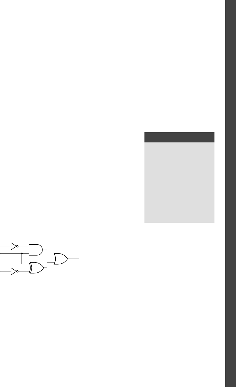
Assertion-Based Design, Harry D. Foster, Adam C. Krolnik, David
J. Lacey, Kluwer Academic Publishers, 2003. Presents a design
methodology based on incorporating assertions into design to make
verification more tractable.
Digital Logic Pocket Data Book, Texas Instruments, 2002. A listing of
the manufacturer’s digital logic components, including basic and
complex gates. Available from www.ti.com.
exercise 2.1 Derive truth tables for the following Boolean expressions:
a) a b
_
c
b) x ⊕ y ⊕ z
c) (a b )
___
(c d)
exercise 2.2 Draw schematic circuit diagrams for the combinational
circuits described by each of the Boolean expressions in Exercise 2.1.
exercise 2.3 Given the truth table in Table 2.10, write a Boolean expres-
sion for the function f, expressed as a sum of minterms.
exercise 2.4 Draw a schematic circuit diagram for the combinational
circuit described by the truth table in Table 2.10.
exercise 2.5 Derive a truth table for the Boolean function implemented
by the circuit in Figure 2.24.
EXERCISESEXERCISES
exercise 2.6 Derive Boolean expressions for the circuit in Figure 2.24,
both directly from the circuit and in the form of a sum of minterms from the
truth table.
exercise 2.7 Derive a truth table for the majority function M that is 1
when two or more of the inputs a, b and c are 1, and 0 otherwise.
exercise 2.8 Show, using truth tables, that the two Boolean expressions
in each of the following pairs are equivalent:
a) x
___
(y z) and x
_
y x
_
z
b)
___
x ⊕ y and
___
_
x ⊕
_
y
x
y
z
f
FIGURE 2.24
Exercises
CHAPTER TWO 83
abcf
0001
0010
0100
0111
1001
1010
1100
1110
TABLE 2.10

exercise 2.9 Draw a schematic for a buffer tree to drive 12 inputs from a
source, assuming that the source and each buffer can each drive at most three inputs.
exercise 2.10 Reduce the size of the truth table in Table 2.11 by using
the don’t care notation for inputs.
exercise 2.11 The truth table in Table 2.12 uses the don’t care notion
for the output. Add four columns to the truth table, one for each of the possible
assignments of 0 or 1 as the actual output for the don’t care combinations.
exercise 2.12 Figure 2.9 shows circuits whose equivalence follows from
the associative laws in Equations 2.3 and 2.4. Draw circuits that similarly follow
from the distributive laws in Equations 2.5 and 2.6.
exercise 2.13 Prove the identity laws (Equations 2.13 and 2.14) and
the absorption laws (Equations 2.15 and 2.16) using just the axioms of
Boolean algebra.
exercise 2.14 Use the laws of Boolean algebra to transform the Boolean
equation
____
(w y) ( x
_
z) into sum-of-products form.
exercise 2.15 Use the laws of Boolean algebra to prove that the Boolean
expressions
_
a bca
_
b cab
_
c abc and abbca c are equivalent.
exercise 2.16 For each of the following Boolean equations, write a
Verilog model for a circuit that implements the equation.
a) m ab b c a c
b) s
___
(x y) ( x
_
z)
c) y (a ⊕ b) (a c)
exercise 2.17 Devise a minimal-length binary code to represent the state
of a phone: on-hook, dial-tone, dialing, busy, connected, disconnected, ringing.
exercise 2.18 Write a Boolean equation involving the bits of the code
in Exercise 2.17 that determines when the phone is off-hook (that is, in a state
other than on-hook or ringing).
exercise 2.19 Devise a one-hot code for the state of a phone, described
in Exercise 2.17.
exercise 2.20 Develop a Verilog model for a circuit that has an input
representing the state of the phone described in Exercise 2.17 and an output that
is 1 when the phone is off-hook.
84 CHAPTER TWO combinational basics
abcf
0000
0011
0100
011–
100–
1011
1101
1110
TABLE 2.12
xyz f
0001
0011
0100
0110
1001
1011
1101
1111
TABLE 2.11

exercise 2.21 Revise the Boolean equations of Example 2.12 so that no
light is activated for invalid code words.
exercise 2.22 Draw circuit diagrams of parity trees, similar to those in
Figure 2.14, but generating and checking odd parity for an 8-bit code.
exercise 2.23 Devise an example using an 8-bit code word to show that
even parity and odd parity cannot be used to detect two separate bit flips in a
code word.
exercise 2.24 Write Boolean equations for a decoder for the code used
in the burglar alarm of Example 2.14.
exercise 2.25 Develop a Verilog model of a decoder for the code used in
the burglar alarm of Example 2.14.
exercise 2.26 Write Boolean equations for an ordinary (nonpriority)
encoder for the code used in the ink-jet printer described in Example 2.9. For
each pair of inputs, determine the code word output of the encoder if the two
inputs are both 1.
exercise 2.27 Develop a Verilog model of a priority encoder for the code
used in the ink-jet printer described in Example 2.9.
exercise 2.28 Write Boolean equations for a BCD decoder, that is, a
decoder that has a BCD code word as input and that has outputs y
0
through y
9
.
Draw a circuit that uses AND and OR gates and inverters to implement the decoder.
exercise 2.29 Develop a Verilog model of the BCD decoder described in
Exercise 2.28.
exercise 2.30 Write Boolean equations for a 2-to-1 multiplexer. Draw a
circuit that uses AND and OR gates and inverters to implement the multiplexer.
exercise 2.31 Use a 2-to-1 multiplexer to implement a circuit whose
output is given by the Boolean expression
a (b +
_
c ) when enable
__
sel is 1, and by
the Boolean expression
x ⊕ y otherwise.
exercise 2.32 Develop a Verilog model of a circuit with the behavior
described in Exercise 2.31.
exercise 2.33 Draw a circuit diagram for a multiplexer that selects
among four sources of data, each of which is encoded with three bits. The circuit
should be implemented 4-to-1 multiplexers (see Figure 2.17).
Exercises CHAPTER TWO 85

86 CHAPTER TWO combinational basics
exercise 2.34 Develop a Verilog model of the multiplexer described in
Exercise 2.33.
exercise 2.35 Revise the vat buzzer circuit of Figure 1.5 so that the low-
level sensor inputs and the buzzer output use active-low signals.
exercise 2.36 Revise the Verilog models of the vat buzzer from Exam-
ples 1.5 and 1.6 so that the low-level sensor input ports and the buzzer output port
use active-low logic.
exercise 2.37 Develop a Verilog testbench model for the vat buzzer from
Example 1.5 and Example 1.6. Include test cases to ensure that the buzzer is
activated when required, and not activated otherwise.
87
numeric basics
One of the most common kinds of information processed by digital
systems is numeric information. In this chapter, we will examine various
binary codes for unsigned integers, signed integers, fixed-point fractions
and floating-point real numbers. For each kind of code, we will describe
how some arithmetic operations can be performed. We will also look at
combinational circuits that implement arithmetic operations, and discuss
trade-offs among different circuits that perform the same operation.
3.1 UNSIGNED INTEGERS
In many applications of digital electronics, we deal with signals that only
take on nonnegative integer values. Some signals may be representations
of real-world information, for example, the temperature set on a thermo-
stat. Other signals may arise as a consequence of the way we organize the
digital system, for example, as numeric indices for tables of information
stored in the system’s memory. In this section, we start with the most
common representation for nonnegative integers, then describe arithmetic
operations using that representation. We will finish the section by looking
at an alternative representation that is used in some systems.
3.1.1 CODING UNSIGNED INTEGERS
We are all familiar with decimal positional representation of numbers.
A decimal number such as 124
10
denotes the sum of 1 hundred, 2 tens
and 4 units. We use the subscript notation to specify that the number is
to be interpreted as decimal, that is, base 10. The position of each digit in
the number determines the power of 10 by which the digit is multiplied,
starting with 10
0
for the right-most digit, 10
1
for the next digit to the left,
and increasing by successive powers of ten for further digits from right to
left. Thus, we write
3

88 CHAPTER THREE numeric basics
124
10
1 10
2
2 10
1
4 10
0
In most applications that deal with nonnegative integers, the natural
way to represent the numeric values is using unsigned binary numbers.
Unsigned binary representation works in the same way as decimal repre-
sentation, except that we only use the binary digits 0 and 1 and we mul-
tiply digits by powers of 2 instead of powers of 10. We can represent the
same numeric value as 124
10
in binary by determining the powers of two
that sum to the number, namely,
124
10
1 2
6
1 2
5
1 2
4
1 2
3
1 2
2
0 2
1
0 2
0
1111100
2
So, to represent this number in a digital system, we would need seven
single-bit signals, each carrying one bit of the binary number. In general,
we represent a number x using n bits x
n 1
, x
n 2
, . . . , x
0
, with
x x
n 1
2
n 1
x
n 2
2
n 2
...
x
0
2
0
example 3.1 What number is represented by the unsigned binary
number 101101
2
?
solution Express the number as a sum of powers of two and calculate
the result:
101101
2
1 2
5
0 2
4
1 2
3
1 2
2
0 2
1
1 2
0
1 32 0 16 1 8 1 4 0 2 1 1
45
10
Our discussion of binary codes in Section 2.2 applies equally to
unsigned binary representation of numbers, since that is just one particu-
lar binary code. Thus, given an n-bit unsigned binary code, we can repre-
sent 2
n
distinct numbers. The smallest number has all 0 bits, representing
the number 0, and the largest number has all 1 bits, representing
1 2
n 1
1 2
n 2
...
1 2
1
1 2
0
2
n
1
Conversely, if we need to represent numbers between 0 and N 1,
we need at least ⎡log
2
N⎤ bits for the unsigned binary representation. In
computer systems, unsigned binary numbers are typically 8, 16 or 32 bits
long, allowing representation of numbers up to 256, over 65,000, and
over 4 billion, respectively. However, when we are designing a digital sys-
tem with no other constraints applied to the number of bits, we would
typically choose the smallest number of bits that can represent the range
of numbers we expect to encode. There is no reason why this should not
be a number of bits other than 8, 16 or 32, such as 5, 17 or 26.

example 3.2 Suppose we are designing a scientifi c instrument to measure
the time interval between two random events very precisely, with a resolution of
nanoseconds (1ns 10
9
seconds). Events may occur as much as a day apart.
How many bits are needed to represent the interval as a number of nanoseconds?
solution There are 10
9
nanoseconds per second, and 606024 86,400
seconds per day, so the largest number we need to allow for is 8.64 10
13
. The
number of bits needed is
⎡log
2
(8.64 10
13
)⎤
⎡
log(8.64 10
13
)
log 2
⎤
⎡46.296 . . .⎤ 47
So at least 47 bits are needed.
Unsigned Integers in Verilog
We saw in Section 2.1.3 that we can use vectors to model binary coded
data. Since unsigned binary is just one form of binary code, we can use
vectors for numeric data also, specifying ranges of index values for nets,
variables and ports, and using indexing to refer to individual bits. When
we look at arithmetic operations on unsigned integers, we will see how
they can be modeled in Verilog as operations on vectors.
example 3.3 Develop a Verilog model of a 4-to-1 multiplexer that selects
among four unsigned 6-bit integers.
solution The module definition is
module multiplexer_6bit_4_to_1
( output reg [5:0] z,
input [5:0] a0, a1, a2, a3,
input [1:0] sel );
always @*
case (sel)
2'b00: z = a0;
2'b01: z = a1;
2'b10: z = a2;
2'b11: z = a3;
endcase
endmodule
3.1 Unsigned Integers
CHAPTER THREE 89

90 CHAPTER THREE numeric basics
This is much the same as the multiplexer model that we saw in Section 2.3.2.
The input ports
a0 through a3 and the output port z are all 6-bit unsigned vec-
tors, indexed from 5 down to 0. We choose this index range so that the index
of each bit in a vector corresponds to the power of its binary weight. The input
port
sel, used to select among the inputs, is also a vector, though we are not
interpreting it as representing a number.
Octal and Hexadecimal Codes
We have seen that we need at least approximately log
2
N bits to represent
the number N in unsigned binary form. The same number is represented
in decimal with approximately log
10
N digits. Now
log
2
N log
10
N/ log
10
2 log
10
N/0.301 . . . log
10
N 3.32 . . .
In other words, we need more than three times as many binary digits
as decimal digits to represent a given number. While that is not necessarily
a problem in terms of the digital system, it is cumbersome and error prone
for us to write down and read the long strings of bits required for large
numbers. For this reason, we often use hexadecimal (base 16) or, less
commonly, octal (base 8) for those purposes. We will show how these
representations work first, then discuss the advantages of using them.
Octal is just another form of positional number system, except that
we use the digits 0 through 7 and multiply them by powers of 8 depending
on their position. Thus, for example,
253
8
2 8
2
5 8
1
3 8
0
2 64 5 8 3 1
128 40 3 171
10
More important, for a given octal number, we can factor out powers
of two in each digit and so very quickly determine the binary representa-
tion of the same number. For example,
253
8
2 8
2
5 8
1
3 8
0
(0 2
2
1 2
1
0 2
0
) 8
2
(1 2
2
0 2
1
1 2
0
) 8
1
(0 2
2
1 2
1
1 2
0
) 8
0
(0 2
2
1 2
1
0 2
0
) 2
6
(1 2
2
0 2
1
1 2
0
) 2
3
(0 2
2
1 2
1
1 2
0
) 2
0
(0 2
8
1 2
7
0 2
6
) (1 2
5
0 2
4
1 2
3
)
(0 2
2
1 2
1
1 2
0
)
010101011
2
In general, given an octal number, we can replace each digit with the
corresponding three binary digits to give the unsigned binary represen-
tation of the number. The three-bit patterns corresponding to the octal
digits are
0: 000 1: 001 2: 010 3: 011 4: 100 5: 101 6: 110 7: 111
Note that we need to take care when using an octal number for an
unsigned binary code if the code is not a multiple of three in length. We
need to understand or specify explicitly how long the binary code is and
drop unused bits from the left when converting from octal. For example,
had we specified that the number 253
8
stood for an 8-bit binary number,
we would have dropped the left-most bit to get 10101011
2
. If any of
the bits we drop from the left are 1 rather than 0, the octal number is
greater than the largest number that can be encoded in the given number
of bits. Usually, this is considered an error.
We can also work in the reverse direction from an unsigned binary
number. We divide the bits in to groups of three, starting from the right,
and replace each group with the corresponding octal digit. For example,
given the unsigned binary number 11001011, we can convert it to octal
as follows:
11001011
2
⇒ 11 001 011 ⇒ 313
8
Note that in this example, the number of bits is not a multiple of
three, so we had to assume a 0 bit on the left. Again, we need to take care
that the actual number of bits in the unsigned binary representation is
understood or explicitly stated.
Hexadecimal is another form of positional number system, like octal,
but based on powers of 16. The only minor problem we encounter is
that we need digits with values from 0 through 15. We use the normal
digits 0 through 9, but augment them with the letters A through F for the
remaining digits. The correspondence is
A
16
10
10
B
16
11
10
C
16
12
10
D
16
13
10
E
16
14
10
F
16
15
10
Thus, for example,
3CE
16
3 16
2
12 16
1
14 16
0
3 256 12 16 14 1
768 192 14 974
10
By similar arguments to those for octal numbers, we can arrive at a
quick method for converting between hexadecimal and unsigned binary
representations of a number. Whereas for octal, we formed groups
of three bits (since 8 2
3
), for hexadecimal we form groups of 4 bits
(since 16 2
4
). The 4-bit patterns corresponding to the hexadecimal
digits are
3.1 Unsigned Integers CHAPTER THREE 91
92 CHAPTER THREE numeric basics
0: 0000 1: 0001 2: 0010 3: 0011 4: 0100 5: 0101 6: 0110 7: 0111
8: 1000 9: 1001 A: 1010 B: 1011 C: 1100 D: 1101 E: 1110 F: 1111
Thus, for example, 3CE
16
0011 1100 1110
2
. In the reverse direction:
11001011
2
⇒ 1100 1011 ⇒ CB
16
As we mentioned earlier, nearly all computer systems use number
representations that are 8, 16 or 32 bits long. Hence, the term byte
for 8 bits of data has entered the common language. Since these are all
multiples of 4 in length and not multiples of 3, hexadecimal is a more
natural representation to convert to than octal. (Engineers sometimes use
the term nibble to refer to 4 bits of data, punning on the fact that a nibble
is a small bite.) With hexadecimal in these applications, we don’t need to
worry about assuming or dropping leading 0 bits. That’s why program-
mers usually deal with hexadecimal and not octal. However, since we,
as hardware designers, can select the number of bits that is best for our
needs, we may find octal more useful in some cases, particularly if the
number of bits is a multiple of 3.
3.1.2 OPERATIONS ON UNSIGNED INTEGERS
Since unsigned integers are binary coded, we can perform on them all
of the operations on encoded data described in Section 2.3. A common
application is to decode an n-bit unsigned binary number representing the
location of information in a memory. The decoder has 2
n
control outputs,
which we can use to activate a particular memory location. We shall see
this in more detail in Chapter 5. We can also use multiplexers in parallel,
one per bit of an unsigned binary representation, to choose between
multiple sources of numeric data. This was illustrated in Example 3.3.
We should also expect to be able to perform arithmetic operations on
numbers represented in unsigned binary. However, before we look at that,
we will discuss some simpler operations.
Resizing Unsigned Integers
When we write numbers in decimal on paper, we usually don’t write any
leading insignificant zeros. We just use the least number of digits needed to
represent the number. For example, we just write 123
10
, and not 0123
10
or 000123
10
, although all represent the same number. We could do the
same in binary, and just write 10110
2
, and not 010110
2
or 00010110
2
.
However, in a digital circuit, each bit is implemented by a physical wire,
and we choose the number of bits based on the largest value we expect
to occur during operation of the circuit. Since wires do not come and go
as values change, we normally do write leading insignificant zeros for
unsigned binary numbers occurring in a digital circuit.
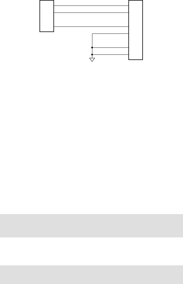
Recall that the largest value that can be represented with n bits is
2
n
1. Suppose we have some numeric data x represented with n bits:
x x
n
1
2
n
1
x
n
2
2
n
2
.
.
.
x
0
2
0
However, in order to perform some arithmetic operations, which may
result in larger values than 2
n
1, we need to represent the same value in
m bits, where m n:
y y
m
1
2
m
1
.
.
.
y
n
2
n
y
n
1
2
n
1
y
n
2
2
n
2
.
.
.
y
0
2
0
Since we want y x, we can just set y
i
x
i
, for i 0, 1, . . . , n 1, and y
i
0,
for i n, n 1, . . . , m 1. In other words, we just add leading insignificant
0 bits to the left of the n-bit representation to form the m-bit representa-
tion. In terms of circuit implementation, we simply add extra bit signals
with their value hard-wired to 0, usually by connecting them to the circuit
ground, as shown in Figure 3.1. This technique is called zero extension.
We can express zero extension in a Verilog model by concatenating a
string of 0 bits to the left of a vector representing an unsigned integer. For
example, given nets declared as
wire [3:0] x;
wire [7:0] y;
We can write the following assignment statement in a module to zero
extend the value of x and assign it to y:
assign y = {4 ' b0000, x};
The notation that we have used here simply joins two vector values
together to form a larger vector. For example, if x has the value 1010,
the value assigned to y would be 00001010. As a convenience, Verilog
3.1 Unsigned Integers CHAPTER THREE 93
FIGURE 3.1 Implementation
of zero extension in a circuit.
x
0
…
……
x
1
x
n − 1
y
0
y
1
y
n − 1
y
n
y
m − 2
y
m − 1

94 CHAPTER THREE numeric basics
automatically zero extends a literal vector value to the specified size. So
we could rewrite the above assignment as
assign y = {4 'b0, x};
In this case, Verilog extends the bit value 0 with additional 0 bits to make
a total of 4 bits.
Verilog also allows us to perform zero extension implicitly. If we assign
an unsigned vector of a smaller size to a vector net or variable of a larger
size, the value is implicitly zero extended to the size of the assignment tar-
get. For example, we could have written the above assignment simply as
assign y = x;
in which case the 4-bit value of x would be implicitly zero extended to
8 bits, the size of y. While this might appear to be a more succinct and
convenient way to write the assignment, we should be aware that zero
extension occurs. Using the vector concatenation operation makes the
extension explicit, which better documents our design intent.
The converse operation to zero extension is truncation, in which we
reduce the number of bits used to represent a numeric value from m to a
smaller size, n. Recall again that the largest value representable in n bits
is 2
n
1. Any m-bit value less than or equal to this value has 0 for all
of the left-most m n bits. So to represent the value in n bits, we simply
discard the left-most m n bits. The problem that might arise is that
the value represented in m bits might be larger than 2
n
1, and so not
be representable in n bits. Such a value has at least one of the left-most
m n bits being 1. In most applications where we need to truncate, this
situation does not arise, and we can discard the bits with impunity. We
only reduce the number of bits when we know that the value must be
within the range representable by the smaller number of bits. We might
arrive at that conclusion by analyzing the arithmetic operations per-
formed to derive the larger-sized value. In terms of circuit implementa-
tion, discarding bits does not mean physically removing anything from
the circuit. Rather, we just leave the left-most bits unconnected, as illus-
trated in Figure 3.2.
An alternative view of truncation of y from m bits to n bits is that it
implements the operation y mod 2
n
. We can demonstrate this as follows:
y mod 2
n
( y
m 1
2
m 1
. . .
y
n
2
n
y
n 1
2
n 1
. . .
y
0
2
0
) mod 2
n
((y
m
1
2
m
n
1
. . .
y
n
2
0
)2
n
y
n
1
2
n
1
. . .
y
0
2
0
) mod 2
n
y
n
1
2
n
1
. . .
y
0
2
0
Thus, if we want to compute y mod 2
n
, we just truncate y to n bits,
regardless of the values of any of the discarded bits.
In a Verilog model, we express truncation of a value by picking
out a part select of the net or variable representing the value. For
example, given nets x and y declared as above, we can write the fol-
lowing assignment statement in a module to truncate the value of y
and assign it to x:
assign x = y[3:0];
The range of values in brackets specifies the index positions of the right-
most elements that we want to use for the smaller representation. For
example, if y has the value 00001110, the value assigned to x would be
1110.
Addition of Unsigned Integers
The addition operation on unsigned binary integers is analogous to the
operation on decimal numbers. We start with the two least significant
operand bits and add them to form the least significant sum bit and a
carry into the next position. We then repeat until we reach the most sig-
nificant position, forming the most significant sum bit and the carry out.
The difference between doing this in binary and decimal is that, in binary,
the sum of the two operand bits and the carry into a position is either 0,
1, 2 or at most 3. Since bits can only be 0 or 1, the case of the sum being
2 means the sum bit is 0 and the carry out is 1, and the case of the sum
being 3 means the sum bit is 1 and the carry out is 1.
…
y
0
y
1
y
n − 1
x
0
x
1
x
n − 1
y
n
y
m − 2
y
m − 1
……
FIGURE 3.2 Implementation
of truncation in a circuit.
3.1 Unsigned Integers
CHAPTER THREE 95

96 CHAPTER THREE numeric basics
example 3.4 Show the addition of the unsigned binary numbers
1010111100
2
and 0011010010
2
.
solution The addition is shown in Figure 3.3. Here, we have included
the carry-out bit from the most significant position. Since it is 0, the result can
be represented in the same number of bits as the two operands.
example 3.5 Show the addition of the unsigned binary numbers 01001
2
and 11101
2
.
solution The addition is shown in Figure 3.4. Again, we have included
the carry out from the most signifi cant position. However, this time it is 1,
indicating that the result value cannot be represented in the same number of bits
as the operands. If the design in which we are doing this addition requires the
result to be fi ve bits long, the carry out of 1 is an error condition. Alternatively,
if the design allows us to use an extra bit for the result, we can use the carry-out
bit as the extra most signifi cant bit, as indicated in grey. This is the same as if we
had zero extended the operands by one bit.
As these examples show, if we need to represent the result in the same
number of bits as the operands (a not uncommon case), we can use the
carry-out bit from the most significant position to indicate whether an over-
flow condition has occurred. When the bit is 1, the sum bits are incorrect.
Let’s now look at how to design a digital circuit to perform addition
upon unsigned binary numbers. Such a circuit is called, unsurprisingly,
an adder. If we consider the method for addition described above, we see
that for the least significant position, the sum (s
0
) and carry-out (c
1
) bits
are Boolean functions of the two least significant operand bits (x
0
, y
0
). We
can express the functions as Boolean equations:
s
0
x
0
⊕ y
0
c
1
x
0
y
0
(3.1)
A circuit to implement these equations is called a half adder, and can
be constructed with an XOR gate to produce the sum bit and an AND
gate to produce the carry-out bit. The reason it’s only half an adder will
become clear in a moment.
For the remaining bits, at each position i, the sum (s
i
) and carry-out
(c
i 1
) bits are Boolean functions of the operand (x
i
, y
i
) and carry-in (c
i
)
bits. The functions are as shown in the truth table in Table 3.1. They can
also be expressed as Boolean equations, as follows:
s
i
( x
i
⊕ y
i
) ⊕ c
i
(3.2)
c
i
1
x
i
y
i
( x
i
⊕ y
i
) c
i
(3.3)
A circuit that implements these equations is called a full adder, since we
can construct it from two half adders: one to add the two operand bits
01001
0011 10
11101
11001
FIGURE 3.4 Unsigned addi-
tion with carry out of 1.
1010111100
1110001110
0011010010
0011110000
FIGURE 3.3 Unsigned addi-
tion with carry out of 0.
x
i
y
i
c
i
s
i
c
i 1
0000 0
0011 0
0101 0
0110 1
1001 0
1010 1
1100 1
1111 1
TABLE 3.1 Truth table for sum
and carry bits.
and one to add the result of that with the carry-in bit. A small amount of
additional logic is needed to form the carry out. However, this form of full
adder is largely of historical interest, since constraints that apply in most
designs lead to different implementations.
One thing to note about the equations for a full adder is that, if the
carry in, c
i
, is 0, the equations simplify to those for a half adder. A con-
sequence is that we can use a full adder for the least significant position
instead of a half adder simply by setting the carry-in bit to 0. This allows
us to treat all positions uniformly, and will also afford another advantage
that we shall see when we get to signed integer addition and subtraction.
Thus, a complete structure for an adder for unsigned integers consists of
a full adder cell for each bit position, with carry outs chained to carry ins
of adjacent positions, as shown in Figure 3.5. (For arithmetic circuits, we
usually arrange components left-to-right in order of decreasing signifi-
cance, to match the left-to-right order of bits of a number. The arrows
on the carry connections in Figure 3.5 indicate that carry values flow
from right to left, contrary to our usual convention of left-to-right flow.)
The carry out of the most significant position can be used as the most
significant sum bit if the sum is allowed to be longer than the operands.
Otherwise, it can be used as an overflow condition signal.
This kind of adder structure is called a ripple-carry adder. We can
see why it has this name by considering the flow of information through
the structure. At each bit position, the values of the sum and carry out-
puts depend not only on the two operand bit inputs, but also on the
carry from the adjacent less significant position. We can also see this by
examining the Boolean equations for the full adder. They form a recur-
rence relation, so that, ultimately, each sum bit and the final carry-out
bit depend on all of the less significant operand bits. When two operand
values arrive at the adder inputs, each full adder determines a transient
value for its sum and carry-out outputs. However, the full adders have
some propagation delay, since they are just logic circuits. Thus, the carry
out from the least significant position acts as an input to the next posi-
tion after the propagation delay, possibly affecting the output of that
position. Its carry out, after another propagation delay, may affect the
output of the third position. In this way, carry values “ripple” from least
significant to most significant position, possibly affecting sum-bit values
along the way.
full
adder
x
i
s
i
c
i
c
i+1
y
i
full
adder
x
0
s
0
c
0
c
1
y
0
full
adder
x
1
s
1
c
2
y
1
full
adder
x
n–1
s
n–1
s
n
c
n–1
c
n
y
n–1
FIGURE 3.5 Structure of an
adder for unsigned integers using
full adder cells.
3.1 Unsigned Integers
CHAPTER THREE 97
98 CHAPTER THREE numeric basics
In the worst case, the delay from operand values arriving to the sum
value settling is the product of each full adder’s propagation delay and the
number of bits in the unsigned binary representation. If the performance
constraints of the application allow for an addition to be done slowly,
a ripple-carry adder is a simple and effective adder structure. However,
many applications require that arithmetic operations have high perfor-
mance in order to meet timing constraints. In those cases, we can find
alternate adder structures that have less delay, though at the expense of
greater circuit area and power consumption.
We will now outline a couple of ways in which we can improve the
adder performance over that of a ripple-carry adder. As the basis of our
discussion, let’s return to Equations 3.2 and 3.3 and to the truth table in
Table 3.1. For a given position i, we can see the following properties.
If x
i
and y
i
are both 0, then c
i 1
0, regardless of the value of c
i
. In
this case, any carry in to the position is killed. We define a signal for
this condition:
k
i
_
x
i
_
y
i
(3.4)
If one of x
i
and y
i
is 1 and the other is 0, then c
i 1
c
i
. In this case,
the carry in is propagated to the next position. A signal for this
condition is
p
i
x
i
⊕y
i
(3.5)
If x
i
and y
i
are both 1, then c
i 1
1, regardless of the value of c
i
. In
this case, a carry out is generated for the next position. We define a
signal for this condition:
g
i
x
i
y
i
(3.6)
Substituting Equations 3.5 and 3.6 into Equations 3.2 and 3.3 gives
s
i
p
i
⊕c
i
(3.7)
c
i 1
g
i
p
i
c
i
(3.8)
One way in which these reformulated equations help is by exposing
a way of determining the carry values at each position more quickly than
the ripple-carry method. Note that the k
i
, p
i
and g
i
signals only depend
on the operand bit values at their respective positions, so they can be
determined quickly after the operand values arrive at the adder inputs. If
a carry is killed or generated at a given position, we don’t need to wait for
the carry in from less significant positions; we can drive a 0 or 1 carry-out
value immediately. On the other hand, if carry is to be propagated, we
왘
왘
왘
x
i
g
i
p
i
k
i
s
i
c
i
c
i+1
y
i
x
i
p
i
s
i
c
i
c
i+1
y
i
0
1
+V
FIGURE 3.6 Fast-carry-chain
full-adder cells.
3.1 Unsigned Integers
CHAPTER THREE 99
can switch the carry in to the carry out very quickly. These observations
form the basis for the structure of a fast-carry-chain adder, sometimes
also called a Manchester adder.
Figure 3.6 shows two alternate implementations of the full-adder
cell used in such an adder. In the implementation on the left, the box at
the top derives the propagate signal, which drives the select input of a
multiplexer. If p
i
is 0, then the carry is either generated (x
i
and y
i
are both
1) or killed (x
i
and y
i
are both 0). So either of the input bits can be selected
to derive the carry out, without having to wait for the carry in. If p
i
is 1,
then the carry out is the same as the carry in. Like the ripple-carry adder,
in the worst case, the carry has to propagate from the least significant
to the most significant position. However, if the implementation fabric
provides fast multiplexers (which many do), the propagation delay along
this carry chain is much less than that of a chain of gate circuits based
on Equation 3.3. As an example, several FPGA families manufactured by
Xilinx include fast-carry chains using multiplexers, allowing fast-carry-
chain adders to be implemented.
The full-adder cell shown at the right of Figure 3.6 is very similar.
The box at the top derives all of the generate, propagate and kill signals.
These are used to drive the control inputs of electronic switches to derive
the carry-out bit. If g
i
is 1, the carry-out bit is switched to 1; if k
i
is 1, the
carry-out bit is switched to 0; and if p
i
is 1, the carry-out bit is switched
from the carry-in input. Again, in the worst case, a carry may have
to propagate from the least significant to the most significant position.
However, fabrics such as custom or standard-cell ASICs include switch
components that have very small propagation delay, allowing fast-carry-
chain adders to be implemented in this way.
Another way in which we can use the reformulated equations is to
solve Equation 3.8 as a recurrence relation and determine all of the carry
100 CHAPTER THREE numeric basics
x
0
g
0
p
0
p
3
s
3
c
0
c
3
c
4
y
0
x
1
g
1
p
1
y
1
x
2
g
2
p
2
y
2
x
3
g
3
p
3
y
3
p
2
s
2
c
2
p
1
s
1
c
1
p
0
s
0
carry-lookahead generator
FIGURE 3.7 A 4-bit carry-
lookahead adder.
bits at once. Equation 3.8 gives us the equation for c
1
directly. We can
substitute this back into Equation 3.8 to get the equation for c
2
:
c
2
g
1
p
1
( g
0
p
0
c
0
) g
1
p
1
g
0
p
1
p
0
c
0
We can repeat substitution and similarly get the equations for c
3
and c
4
:
c
3
g
2
p
2
g
1
p
2
p
1
g
0
p
2
p
1
p
0
c
0
c
4
g
3
p
3
g
2
p
3
p
2
g
1
p
3
p
2
p
1
g
0
p
3
p
2
p
1
p
0
c
0
Note that each of these expressions is a function of only c
0
and the
operand input bits (since the generate and propagate signals are func-
tions only of the operand bits). This gives us a way to determine the
carry bit at each position without having to wait for carries to propa-
gate up from less significant positions. We can then use the carry bit
to derive the sum bits according to Equation 3.2. An adder based on
this formulation is called a carry-lookahead adder. A 4-bit version of
such an adder is illustrated in Figure 3.7. Each of the boxes at the top
derives the generate and propagate signals for the corresponding bit
position. The carry-lookahead generator implements the equations
shown above to derive the carry signals. These are combined with the
propagate signals to derive the sum bits. The trade-off for getting the
sum bits faster is the area and power consumed by the carry-lookahead
generator circuitry.
We have shown a carry-lookahead generator for 4 bits, since that is
about as large as we can practically make it. In principle, we could con-
tinue substituting in Equation 3.8 to get further carry bits. However, a
more practical approach for wider adders is to use 4-bit carry-lookahead
adders for segments of 4 bits, and to use a second level of carry-lookahead
generators to derive the carry-in bits for each segment. There are also

other forms of adders that build upon the reformulated expressions to
compute carry bits in different ways. The choice among them is a ques-
tion of making trade-offs among circuit area, power and performance,
constrained by the resources available in implementation fabrics. A full
discussion of these adder structures is beyond the scope of this book, but
there are many references that go into detail.
In all of our discussion of adders so far, we have not yet described
how to model them in Verilog. We could simply translate the Bool-
ean expressions in the various forms we have discussed into Verilog.
However, doing so would disguise our design intent of adding unsigned
binary numbers. In particular, a CAD tool would just try to implement
the model as combinational circuitry, and may not readily be able to
recognize the opportunity to use any specialized circuit resources, such
as fast-carry chains, available in an implementation fabric. A much
better approach is to use the addition operator provided by Verilog to
operate on vector values. A synthesis CAD tool can then implement the
addition operation using the most appropriate form of adder provided
by the target fabric to meet design constraints. Alternatively, we could
develop a structural model, selecting the most appropriate form of adder
from a library of arithmetic components, and verify that the structural
model produces the same results as a behavioral model using the addi-
tion operator.
example 3.6 Given the Verilog declaration of three nets:
wire [7:0] a, b, s;
write a Verilog statement to assign the sum of a and b to s.
solution The required statement is
assign s = a + b;
The operator works on two unsigned values to produce an unsigned result
whose length is the larger of the two operands. It does not produce a carry out,
so if there is an overflow, it remains undetected.
example 3.7 Revise the statements to produce a carry-out bit, c.
solution We can do this by zero extending a and b by one extra bit before
doing the additions, in order to get a 9-bit result. The carry out is then
3.1 Unsigned Integers CHAPTER THREE 101

102 CHAPTER THREE numeric basics
the most significant bit of that result, and the 8-bit sum is the remaining bits.
We need to declare a net for the 9-bit intermediate result and for the carry bit:
wire [8:0] tmp_result;
wire c;
The required statements are
assign tmp_result = {1 'b0, a} + {1 'b0, b};
assign c = tmp_result[8];
assign s = tmp_result[7:0];
An alternative way of writing these assignments is
assign {c, s} = {1 'b0, a} + {1 'b0, b};
In this assignment, the left-hand side is written as a concatenation of the carry
bit and sum nets. The bits of the result of addition are assigned to the corre-
sponding bits of the concatenated nets. We can simplify this further, since Verilog
has rules that cover implicit extension of expression operands based on the size
of the left-hand side of an assignment. If we write
assign {c, s} = a + b;
the Verilog rules determine that the size of the left-hand side is 9 bits, so the values
of a and b must be extended to 9 bits. Since they are unsigned values, they are
implicitly zero extended, and the result of the addition is also 9 bits long. As we
mentioned earlier, while these rules might appear to make the assignment more
succinct, we must take care that implicit extensions have the effect we really want.
If in doubt, or if we want to make our intent explicit, we can use explicit extension.
The above example shows how we can use vectors when we need
to access the individual bits of the binary code. Often, we can raise the
level of abstraction in our Verilog model by considering only the numeric
aspects of data and not their binary encoding. Verilog allows us to do so
using the type integer for numbers. We can declare a variable (but not a
net) to be of type integer as follows:
integer n;

Integer variables are typically 32 bits long, though a Verilog implementa-
tion is allowed to use a larger size. The range of values represented by a
32-bit integer includes the unsigned values up to approximately 2 billion.
It also includes negative numbers, which we will discuss further in the
next section.
example 3.8 Revise the declaration and statement in Example 3.6 to use
integer variables instead of vector nets.
solution The revised declaration is
integer a, b, s;
Since we are using variables instead of nets, the assignment must be in a proce-
dural block. We replace the assignment statement with the always block:
always @*
s = a + b;
The addition expression looks exactly like that in the original assignment. The
only difference is that we are not concerned about the size of the variables and
are ignoring the possibility of any carry out. A synthesis tool would infer at least
a 32-bit adder with no overflow checking, since we have not indicated the actual
range of values that can occur. That is one reason why we would not generally
use integer types for synthesizable models where the range of values is known to
be smaller than 32.
Subtraction of Unsigned Integers
We can work out how to perform subtraction of unsigned binary inte-
gers by following a process similar to that for addition. First, we devise
the steps for binary subtraction, bit by bit, analogously to subtraction of
decimal digits. Recall that, in decimal, if we subtract a larger digit from a
smaller digit, we borrow from the next column. We do the same in binary,
borrowing if we subtract 1 from 0.
example 3.9 Show the subtraction of the unsigned binary numbers
10100110
2
and 01001010
2
.
solution The subtraction is shown in Figure 3.8. Here, we have included
the borrow-out bit from the most signifi cant position. Since it is 0, the result
can be represented in the same number of bits as the two operands.
10100110
01011100
0– 1001010
01011000
x:
y:
d:
b:
FIGURE 3.8 Unsigned
subtraction.
3.1 Unsigned Integers
CHAPTER THREE 103

104 CHAPTER THREE numeric basics
Next, we look at how to design a subtracter circuit to perform sub-
traction upon unsigned binary numbers. For the least significant position,
the difference (d
0
) and borrow-out (b
1
) bits are Boolean functions of the
two least significant operand bits. The Boolean equations are
d
0
x
0
⊕y
0
b
1
_
x
0
y
0
For the remaining bits, at each position i, the difference (d
i
) and borrow-out
(b
i1
) bits are Boolean functions of the operand (x
i
, y
i
) and borrow-in (b
i
)
bits, with the truth table shown in Table 3.2. They can also be expressed as
Boolean equations, as follows:
d
i
( x
i
⊕y
i
)⊕ b
i
(3.9)
b
i 1
_
x
i
y
i
____
(x
i
⊕ y
i
) b
i
(3.10)
As we did in the case of the adder, we can set the borrow in for the least
significant position to 0 and just use Equations 3.9 and 3.10 uniformly for all
positions. We could now go ahead and develop circuits for these equations.
However, many systems that need a subtracter also need an adder, and
choose whether to add or subtract the operands. A little algebraic manipu-
lation will expose a trick that allows us to use the same circuit to perform
either addition or subtraction. Notice that the equation for the difference is
the same as that for the sum in an adder, and that the equation for the bor-
row is similar to that for the carry. The trick lies in using the complemented
form of the borrow bits. If we do that, we can rewrite the equations as
d
i
( x
i
⊕
_
y
i
)⊕
_
b
i
(3.11)
___
b
i 1
x
i
_
y
i
( x
i
⊕
_
y
i
)
_
b
i
(3.12)
Proof of this is left to Exercise 3.27. If we compare these equations with Equa-
tions 3.2 and 3.3, we see that they are identical in form, but with
_
y
i
replacing
y
i
and
_
b
i
replacing c
i
. Consequently, we can use an adder circuit to perform
subtraction simply by negating each bit of the second operand and using a
negated form of borrow. For the least significant position, we set the negated
borrow-in bit to 1. We can use the negated borrow out from the most sig-
nificant position to indicate underflow: if it is 0, indicating a borrow, the true
difference is negative, and so cannot be represented as an unsigned integer.
Now let’s see how to modify an adder circuit to perform both addition
and subtraction. Suppose we have a control signal that is 0 when we want
the circuit to perform addition and 1 when we want it to perform subtrac-
tion. Since addition requires a 0 value for the least significant carry in and
subtraction requires a 1 for the least significant negated borrow in, we
can just use the control signal as the carry in/negated borrow in. We could
also use the control signal to control an n-bit 2-to-1 multiplexer selecting
between the second operand and its negation as the second input to the
circuit. However, another part of the trick is to notice that y
i
⊕ 0 y
i
and
y
i
⊕ 1
_
y
i
. So we can connect each bit of the second operand to an XOR
x
i
y
i
b
i
d
i
b
i 1
00 0 0 0
00 1 1 1
01 0 1 1
01 1 0 1
10 0 1 0
10 1 0 0
11 0 0 0
11 1 1 1
TABLE 3.2 Truth table for
difference and borrow bits.
3.1 Unsigned Integers CHAPTER THREE 105
y
0
y
1
y
n–1
y
0
c
0
c
n
y
1
y
n–1
…
…
…
…
x
0
x
1
x
n–1
x
0
x
1
x
n–1
… s
0
s
1
s
n–1
s
n–1
/d
n–1
s
1
/d
1
s
0
/d
0
…
adder
add/sub
ovf/unf
FIGURE 3.9 Adapting an
adder to perform addition and
subtraction.
gate with the control signal as the other gate input, and connect the gate
outputs to the adder. The final circuit for an adder/subtracter is shown in
Figure 3.9. The adder can be any of the circuits we described earlier: ripple-
carry or optimized for the application’s requirements and constraints.
As with Verilog models that perform addition, we normally write
models that apply the subtraction operator to vector values, rather than
directly implementing the Boolean equations for a subtracter. That way,
we can let the synthesis CAD tool decide on an appropriate subtracter
circuit to use depending on constraints that apply. Moreover, if the system
we are designing performs both addition and subtraction, the tool can
decide whether to use separate circuits for the operations, or to share
a single adder/subtracter between the operations. Naturally, it can only
share the circuit if operations are to be done at different times. We shall
see in later chapters how to control sequencing of operations. For now,
we will just consider combinational circuits that assume the existence of a
control signal for selecting between addition and subtraction operations.
example 3.10 Develop a Verilog behavioral model of an adder/subtracter
for 12-bit unsigned binary numbers. The circuit has data inputs
x and y, a data
output s, a control input mode that is 0 for addition and 1 for subtraction, and
an output
ovf_unf that is 1 when an addition overfl ow or a subtraction under-
fl ow occurs.
solution The module performs the addition and subtraction using the
and operators on the vector operand values, as follows:
module adder_subtracter ( output [11:0] s,
output ovf_unf,
input [11:0] x, y,
input mode );
assign {ovf_unf, s} = !mode ? (x + y) : (x – y);
endmodule

106 CHAPTER THREE numeric basics
The assignment in the module uses the mode input to choose between addition
and subtraction of the operands. Since we want to use the carry-out or borrow-
out bit for the
ovf_unf output, we assign to the concatenation of the two outputs
using the notation we saw in Example 3.7. Verilog implicitly extends the addi-
tion and subtraction operands to match the 13-bit size of the assignment target.
The least significant 12 bits of the result are used as the sum or difference output
value and the most significant bit as the
ovf_unf value. In the case of addition,
the most significant bit is the carry out: 1 for overflow, or 0 otherwise. In the
case of subtraction, the most significant bit is the borrow out, not negated: 1 for
underflow, or 0 otherwise. Thus, we can use this bit for the
ovf_unf output.
example 3.11 Develop a verifi cation testbench for the adder/subtracter
that compares the result with the result of addition or subtraction performed on
values of type integer.
solution The module, test_add_sub, has no ports, since it is a self-
contained testbench:
`timescale 1ns/1ns
module test_add_sub;
reg [11:0] x, y;
wire [11:0] s;
reg mode;
wire ovf_unf;
integer x_num, y_num, s_num;
task apply_test ( input integer x_test, y_test,
input mode_test );
begin
x = x_test; y = y_test; mode = mode_test;
#10;
end
endtask
adder_subtracter duv ( .x(x), .y(y), .s(s),
.mode(mode), .ovf_unf(ovf_unf) );
initial begin
apply_test( 0, 10, 0);
apply_test( 0, 10, 1);
apply_test( 10, 0, 0);
apply_test( 10, 0, 1);
apply_test(2**11, 2**11, 0);
(continued)

The module declares nets and variables to connect to the inputs and outputs of
the adder/subtracter instance,
duv. The instance is followed by a task to apply
individual test cases. The initial block makes successive calls to the task to assign
a sequence of input values to the inputs, exercising both addition and subtrac-
tion with cases that produce normal results, overflow and underflow. Note the
use of the value
2**11, which is the way we write 2
11
in Verilog. The ** operator
performs exponentiation.
The always block responds to changes of input values to the adder/
subtracter, then waits for the adder/subtracter to produce outputs. The block
then assigns the unsigned input values to the variables
x_num, y_num and
s_num of type integer. The block then checks the value of the mode input. If
it is 0, indicating addition, the block checks the numeric sum of the oper-
ands. Since it does this using the numeric variables, the result is not limited
to the range representable in 12 bits. Hence, the block can compare the true
sum with the largest value representable in 12 bits, namely, 2
12
1. If the
sum is larger, the block verifies that the
ovf_unf output is 1. Otherwise, the
block verifies that the
ovf_unf output is 0 and that the sum result is equal to
apply_test(2**11, 2**11, 1);
// ... further test cases
#10 $finish;
end
always @* begin
#5
x_num = x; y_num = y; s_num = s;
if (!mode)
if (x_num + y_num > 2**12–1) begin
if (!ovf_unf)
$display("Addition overflow: ovf_unf should be 1");
end
else begin
if (!(!ovf_unf && s_num = = x_num + y_num))
$display("Addition result incorrect");
end
else
if (x_num – y_num < 0) begin
if (!ovf_unf)
$display("Subtraction underflow: ovf_unf should be 1");
end
else begin
if (!(!ovf_unf && s_num = = x_num – y_num))
$display("Subtraction result incorrect");
end
end
endmodule
3.1 Unsigned Integers
CHAPTER THREE 107

108 CHAPTER THREE numeric basics
the computed numeric sum. If mode is 1, indicating subtraction, the block
performs similar checks, but compares the numeric difference between the
operands with 0.
Note that the condition checks and choices between consequent actions in the
always block are written using Verilog if statements. Each if statement has
the form
if ( condition )
statement
else
statement
The first statement is performed if the condition is true, and the second state-
ment is performed if the condition is false. The keyword
else and the the second
statement are optional, and are omitted if there is no action to perform if the
condition is false. Since an if statement is just one form of statement, we can nest
an if statement within an alternative of an outer if statement. The always block
illustrates this: it has an outer if statement,
if (!mode) . . . , that has nested if state-
ments for each of the alternatives. If we need to perform more than one state-
ment in either alternative, we bracket the group of statements in the keywords
begin . . . end, as shown in the example model. We also use begin . . . end
bracketing if a nested if statement omits the else alternative. The bracketing
makes it clear that the else belongs to the outer if statement, not the inner if
statement.
Incrementing and Decrementing Unsigned Integers
There are two further arithmetic operations that we may perform on
unsigned binary integers and that are related to addition and subtrac-
tion. The increment operation involves adding the constant value 1,
and the decrement operation involves subtracting the constant value 1.
These operations arise quite frequently in digital systems, particularly as
part of counters, which generate increasing or decreasing sequences of
numbers.
A straightforward way to design an increment circuit would be to
use an adder with one operand input hard wired to the unsigned binary
representation of 1, namely, 0 . . . 001. Alternatively, we could hard wire
one input to the representation of 0 and the carry in to 1. However, since
one input is a constant value, we can simplify the circuit considerably. To
see how, let’s return to the Boolean equations for an adder, Equations 3.2
and 3.3. If we substitute y
i
0, we can simplify to the equations
s
i
x
i
⊕c
i
c
i 1
x
i
c
i
half
adder
x
i
s
i
c
i
c
i+1
half
adder
x
0
s
0
c
1
half
adder
x
1
s
1
c
2
half
adder
x
n–1
s
n–1
s
n
c
n–1
c
n
+V
FIGURE 3.10 Structure of
an incrementer for unsigned inte-
gers using half adder cells.
3.1 Unsigned Integers
CHAPTER THREE 109
which are essentially those for a half adder (Equation 3.1 on page 96).
In other words, an incrementer can be formed using a chain of half
adders, as shown in Figure 3.10. The carry out of the most significant
bit can be used for an overflow condition signal. A decrementer can be
formed similarly by simplifying the equations for a subtracter with one
input hard wired to the representation of 0 and the negated borrow in
hard wired to 0.
Note that the incrementer of Figure 3.10 is a ripple-carry circuit, and
so has similar delay characteristics to a ripple-carry adder. In the same
way that we improved the performance of adders and subtracters, we
could improve the performance of incrementers and decrementers, for
example, using fast carry chains or carry-lookahead.
In Verilog models, we can express the increment or decrement opera-
tion by adding or subtracting the literal value 1 to an operand. For exam-
ple, given nets declared as
wire [15:0] x, s;
we could assign the incremented value of x to s with the statement
assign s = x + 1;
and we could assign the decremented value with the statement
assign s = x – 1;
Note that the value 1 is a numeric value, represented by Verilog in binary
form. The size of the representation is determined by the context. In this
example, it is 16 bits, since that is the size of the addition and subtraction
operands and the assignment target. Using unsized numeric values like
this is a convenient way to make our Verilog models more concise.
110 CHAPTER THREE numeric basics
Comparison of Unsigned Integers
In some applications, it may be necessary to compare two unsigned binary
integers for equality or inequality. Since there is exactly one code word
for each numeric value, we can test for equality of two unsigned binary
integers by testing whether the corresponding bits of each are the same.
When we introduced the XNOR gate in Section 2.1.1, we mentioned that
it is also called an equivalence gate, since its output is 1 only when its
two inputs are the same. Thus, we can test for equality of two unsigned
binary numbers using the circuit of Figure 3.11, called an equality com-
parator. In practice, an AND gate with many inputs is not workable, so
we would modify this circuit to better suit the chosen implementation
fabric. Better yet, we would express the comparison in a Verilog model
and let the synthesis tool choose the most appropriate circuit from its
library of cells.
Comparing two unsigned binary integers for inequality (greater than
or less than comparison) is somewhat more complicated. To test whether
a number x is greater than another number y, we can start by comparing
the most significant bits, x
n 1
and y
n 1
. If x
n 1
y
n 1
, we know imme-
diately that x y . Similarly, if x
n 1
y
n 1
, we know immediately that
x y. In both cases, the final result is completely determined by compar-
ing just the most significant bits. If x
n 1
y
n 1
, the result depends on
the remaining bits, and is true if and only if x
n 2 . . . 0
y
n 2 . . . 0
. We can
now apply the same argument recursively, examining the next pair of bits,
and, if they are equal, continuing to less significant bits. Note that x
i
y
i
is only true for x
i
1 and y
i
0, that is, if x
i
_
y
i
is true. These consid-
erations lead to the circuit of Figure 3.12, called a magnitude compara-
tor. We can use the same circuit to test for less than inequality simply by
exchanging the operands at the inputs.
In Verilog, we can express comparison operations on unsigned val-
ues using the
, and operators. (Note the distinction between
the equality operator, , and the assignment operation, .) We can
also use ! for “not-equal,” for “less-than or equal,” and for
“greater-than or equal.” All of these operators yield a single-bit 0 or 1
x
0
eq
…
y
0
x
1
y
1
x
n–1
y
n–1
…
FIGURE 3.11 Circuit for an
equality comparator.
result, which can also be interpreted as a Boolean false or true result,
respectively. This is convenient if the comparison occurs in the condition
part of an if statement, since a Boolean result is expected in that context.
It is also convenient if we want to assign the result to a net or variable,
for example:
assign gt = x > y;
example 3.12 Develop a Verilog model for a thermostat that has two
8-bit unsigned binary inputs representing the target temperature and the actual
temperature in degrees Fahrenheit (˚F). Assume that both temperatures are above
freezing (32˚F). The detector has two outputs: one to turn a heater on when the
actual temperature is more than 5˚F below target, and one to turn a cooler on
when the actual temperature is more than 5˚F above target.
solution The module definition is
module thermostat ( output heater_on, cooler_on,
input [7:0] target, actual );
assign heater_on = actual < target – 5;
assign cooler_on = actual > target + 5;
endmodule
x
n–1
gt
x
n–1
> y
n–1
x
n–1
= y
n–1
x
n–2
> y
n–2
x
n–2
= y
n–2
y
n–1
x
n–2
y
n–2
x
1
> y
1
x
1…0
> y
1…0
x
n–2…0
> y
n–2…0
x
1
= y
1
x
1
y
1
x
0
> y
0
x
0
y
0
…
…
…
FIGURE 3.12 A magnitude
comparator to test for greater than
inequality.
3.1 Unsigned Integers
CHAPTER THREE 111

112 CHAPTER THREE numeric basics
The assignments use the subtraction and addition operators to calculate the
thresholds for turning the heater and cooler on. They use the and operators
for performing the comparisons against the thresholds.
Scaling by a Constant Power of 2
Before we turn to multiplying unsigned integers in a general way, let’s
look at the specific case of scaling an unsigned integer by a given constant
value that is a power of 2. The simplest case is multiplying by 2. Recall
that the value x represented by the n bits x
n 1
, x
n 2
, . . . , x
0
is
x x
n 1
2
n 1
x
n 2
2
n 2
. . .
x
0
2
0
(3.13)
If we multiply both sides by 2, we get
2x x
n 1
2
n
x
n 2
2
n 1
. . .
x
0
2
1
(0)2
0
which is an n 1 bit number consisting of the bits of x, shifted left by
one position, and a 0 bit appended as the least significant bit. If we are
working with fixed-length integers, we can truncate the most significant
bit to yield an n-bit number, provided the truncated bit is 0. This opera-
tion is called a logical shift left by one position. We can take this form
of scaling further. To scale by a factor of 2
k
, we repeat the scaling-by-2
process k times. That is, we shift the bits left by k positions and append
k bits of 0 to the least significant end. If we need to truncate to an n-bit
result, the k truncated bits must all be zero; otherwise an overflow has
occurred.
Dividing by 2 works similarly. If we divide both sides of Equation 3.13
by 2 we get
x/2 x
n 1
2
n 2
x
n 2
2
n 3
. . .
x
1
2
0
x
0
2
1
Since 2
1
is the fraction ½, and we are dealing with integers only, we can
discard the last term in this equation. The result is an n 1 bit number
consisting of the bits of x, except for the least significant bit, shifted right
by one position. If we are working with fixed-length integers, we can
append a 0 to the most significant end to maintain the value. This opera-
tion is called a logical shift right by one position.
We can take this further also. To divide by 2
k
, we shift the bits right
by k positions, discarding the k least significant bits and appending k bits
of 0 at the most significant end. If any of the discarded bits were nonzero,
the true result of the division is truncated toward 0.
Verilog provides two operators for shifting the bits of an unsigned
value. The operator performs a logical shift left, and the operator
performs a logical shift right. For example, if the unsigned net or vari-
able s has the value 00010011, representing the value 19
10
, the Verilog
expression

s << 2
would yield the value 01001100, representing the value 76
10
. The
expression
s >> 2
would yield the value 00000100, representing the value 4
10
.
Multiplication of Unsigned Integers
The final arithmetic operation on unsigned integers that we shall examine
is multiplication. A straightforward approach for multiplying x by y is to
expand the product out as follows:
xy x(y
n 1
2
n 1
y
n 2
2
n 2
. . .
y
0
2
0
)
y
n 1
x2
n 1
y
n 2
x2
n 2
. . .
y
0
x2
0
The largest value of the product is the product of the largest values of the
operands. For n-bit operands, that is
(2
n
1)(2
n
1) 2
2n
2
n
2
n
1 2
2n
(2
n 1
1)
which requires 2n bits to represent. If we provide this many bits for the
product, there is no possibility of overflow.
Each of the terms in the expanded product equation is called a
partial product, and consists of the product of a bit y
i
, the number x
and 2
i
. Recall that x2
i
is just the bits of x shifted left by i positions. Also,
y
i
is either 0 or 1. If it is 0, the partial product is 0. If it is 1, the partial
product is just the shifted version of x. Thus the partial product can be
formed by AND-ing each bit of x with y
i
and adding it, shifted i places
to the left, into the final product. The addition of the partial prod-
ucts can be performed by a series of adders, as shown in Figure 3.13.
This is a basic form of combinational multiplier, so called because it
is a combinational circuit (albeit a large one). In Chapter 4, we will
look at techniques that allow us to construct a sequential multiplier, in
which we add partial products one at a time in successive clock cycles.
A sequential multiplier trades off reduced area against time taken to
yield the product.
In the multiplier circuit of Figure 3.13, we have not specified what
kind of adder to use. We could use any of the adders we discussed
earlier, with the choice depending on the performance requirements
and area constraints that apply. We could also optimize the circuit by
3.1 Unsigned Integers CHAPTER THREE 113
114 CHAPTER THREE numeric basics
combining parts of adjacent adders to reduce the overall propagation
delay through the structure. However, techniques for doing so are
beyond the scope of this book. They are discussed in detail in books
cited for further reading in Section 3.6. For our purposes, we will rely
on a synthesis CAD tool selecting an appropriate multiplier from the
resources available to it.
As with other arithmetic operations on unsigned binary integers, we
represent multiplication in Verilog models using an operator on unsigned
x
0
y
1
x
1
x
n–1
y
0
c
0
c
n
y
1
y
n–1
y
n–2
…
……
x
n–2
x
0
x
1
x
n–2
… s
0
s
1
s
2
x
n–1
…
s
n–1
… s
1
s
2
…
…
…
…
s
n–1
adder
x
0
y
2
x
1
x
n–1
y
0
c
0
c
n
y
1
y
n–1
y
n–2
…
…
…
…
x
n–2
x
0
x
1
x
n–2
s
0
x
n–1
…
adder
… s
1
s
2
…
s
n–1
x
0
y
0
x
1
x
n–1
y
0
c
0
c
n
y
1
y
n–1
y
n–2
…
…
…
…
x
n–2
x
0
x
1
x
n–2
s
0
x
n–1
adder
… s
1
s
2
…
s
n–1
x
0
y
n–1
x
1
x
n–1
y
0
c
0
c
n
y
1
y
n–1
y
n–2
…
…
…
…
x
n–2
p
0
p
1
p
2
p
n–1
p
n
p
n+1
p
2n–2
p
2n–1
x
0
x
1
x
n–2
s
0
x
n–1
adder
FIGURE 3.13 A combina-
tional multiplier constructed from
adders for partial products.

values. The result of the * operator is an unsigned vector whose length
is the larger of the operand lengths. If we need the multiplication to be
performed with size that is the sum of the operand lengths, in order not
to overflow, we must extend the operand values before multiplying them.
For example, given the following declarations:
wire [ 7:0] x;
wire [13:0] y;
wire [21:0] p;
we could assign the product of x and y to p with the following
statement:
assign p = {14'b0, x} * {8'b0, y};
Alternatively, we could rely on Verilog’s implicit zero extension and just
write:
assign p = x * y;
Summary of Arithmetic Operations
In this section, we have examined several arithmetic operations that can
be performed on unsigned binary integers, including addition, subtrac-
tion and multiplication. We have deliberately avoided division, since it
is considerably more complex to implement than the other operations,
and arises less frequently in real-world applications. Hence, there are
relatively few application-specific digital systems that include circuits for
performing division. Division circuits are described in the books cited in
Section 3.6.
In our discussion, we focused on addition as a foundational operation
and examined a number of adder circuits that trade off between perfor-
mance and circuit area. This is a recurring theme in digital design, and is
well illustrated through consideration of adder circuits. We return to it
throughout this book.
For each operation, we also discussed how to represent the opera-
tion in Verilog models that use unsigned vectors. This approach allows
us to abstract away from the details of the digital circuits that implement
the arithmetic operations, relying on synthesis CAD tools to choose
appropriate circuits from libraries of cells that can be implemented in
3.1 Unsigned Integers CHAPTER THREE 115
116 CHAPTER THREE numeric basics
the target fabric. As we shall see when we describe our implementation
methodology in more detail, we separate the concerns of specifying
the circuit behavior in Verilog and constraining the implementation.
We provide speed and area constraints for use by the synthesis tool
to determine an appropriate implementation. This approach helps us
manage the complexity of designing systems to perform numerical
computation.
3.1.3 GRAY CODES
The binary code that we have considered so far in this section is not the
only code for unsigned integers, though it is the most natural code to use
when we need to perform arithmetic operations. However, it has some
disadvantages in other applications. Consider a scenario in which we are
to design a system that uses a binary code to represent the angular posi-
tion of a rotating shaft. A common way to measure the position is with
a shaft encoder, illustrated in Figure 3.14. The disk attached to the shaft
has a number of concentric bands, each of which has opaque parts and
transparent parts. For each band, there is a light emitter and a detector.
The detector output is 1 when the light shines through the transparent
part of the band and 0 when the light is obscured by the opaque part of
the band. The collection of four decoder outputs forms a binary code for
the angular position of the shaft.
The pattern of transparency and opacity in the bands on the disk
is shown in Figure 3.15, and corresponds to a 4-bit Gray code, in
which adjacent code words differ by only one bit. A complete rota-
tion is divided into 16 segments, and between any two adjacent seg-
ments, exactly one band changes between transparent and opaque. This
prevents any minor error in positioning of the detectors from caus-
ing incorrect position codes. Suppose, in contrast, that we used the
unsigned binary code of Section 3.1.1 for the angular position. This
would give a code word of 0011 for segment 3 and 0100 for segment
4. A minor error in position of the detector for the second band might
cause it to sense the change from 0 to 1 before the detectors for the
right two bands sense the changes from 1 to 0. This would give a code
word of 0111, representing segment 7, for the angular position close to
the boundary between segments 3 and 4. It is difficult to manufacture
mechanical components with sufficient precision to avoid this kind of
error. The Gray code, on the other hand, is much more tolerant of posi-
tioning error, and so is widely used in electromechanical components
that measure position.
The 4-bit Gray code we have used in this example scenario is listed,
along with the corresponding decimal and unsigned binary codes, in
Table 3.3. Note how adjacent Gray code words differ in only one bit
FIGURE 3.14 An optical
shaft encoder.
0000
00010101
1100 1000
10011101
1111 1011
1110 1010
0111 0011
0110 0010
0100
FIGURE 3.15 Gray code
pattern on a shaft-encoder disk.

3.1 Unsigned Integers CHAPTER THREE 117
position, unlike the corresponding unsigned binary code words. This is
not the only 4-bit Gray code; there are others that also have the property
of single-bit difference between adjacent code words. The code we have
used here is generated by the following rules, which allow us to generate
an n-bit Gray code:
A 1-bit Gray code has the two code words 0 and 1.
The first 2
n 1
code words of an n-bit Gray code consist of the
code words of an (n 1)-bit Gray code, in order, each with a 0 bit
appended as the left-most bit.
The last 2
n 1
code words of an n-bit Gray code consist of the code
words of an (n 1)-bit Gray code, in reverse order, each with a 1 bit
appended as the left-most bit.
example 3.13 Develop a Verilog model of a code converter to convert
the 4-bit Gray code to a 4-bit unsigned binary integer.
왘
왘
왘
decimal unsigned
binary
gray code
0 0000 0000
1 0001 0001
2 0010 0011
3 0011 0010
4 0100 0110
5 0101 0111
6 0110 0101
7 0111 0100
8 1000 1100
9 1001 1101
10 1010 1111
11 1011 1110
12 1100 1010
13 1101 1011
14 1110 1001
15 1111 1000
TABLE 3.3 4-bit Gray code,
compared to unsigned binary code.

118 CHAPTER THREE numeric basics
solution For the both the Gray-code input to the converter and the
binary-code output, we use vector ports. The module definition is
module gray_converter ( output reg [3:0] numeric_value,
input [3:0] gray_value );
always @*
case (gray_value)
4'b0000: numeric_value = 4'b0000;
4'b0001: numeric_value = 4'b0001;
4'b0011: numeric_value = 4'b0010;
4'b0010: numeric_value = 4'b0011;
4'b0110: numeric_value = 4'b0100;
4'b0111: numeric_value = 4'b0101;
4'b0101: numeric_value = 4'b0110;
4'b0100: numeric_value = 4'b0111;
4'b1100: numeric_value = 4'b1000;
4'b1101: numeric_value = 4'b1001;
4'b1111: numeric_value = 4'b1010;
4'b1110: numeric_value = 4'b1011;
4'b1010: numeric_value = 4'b1100;
4'b1011: numeric_value = 4'b1101;
4'b1001: numeric_value = 4'b1101;
4'b1000: numeric_value = 4'b1111;
endcase
endmodule
The module’s behavior takes the form of a truth table. It uses the Gray-code
value to select which unsigned numeric value to assign to the output.
1. How is a number x represented in binary as a sum of powers of 2?
2. What range of values can be represented as an n-bit unsigned binary
number?
3. Write a Verilog declaration for a net x to represent unsigned
numbers in the range 0 to 8191.
4. Write the binary number 01011101 in octal and in hexadecimal.
5. Resize the unsigned binary number 10010011 to 12 bits and to 6
bits. In each case, does the result correctly represent the same value
as the original number?
6. Add the two 8-bit unsigned binary numbers 01001010 and
01100000 to get an 8-bit result. Does the addition overfl ow?
7. What distinguishes a ripple-carry adder from a carry-lookahead
adder?
KNOWLEDGE
TEST QUIZ
KNOWLEDGE
TEST QUIZ
8. Write Verilog assignments to add two nets s1 and s2 of type wire
[15:0]
to get a result net s3 of the same type as s1 and s2 and a
carry-out net c_out.
9. Perform the 8-bit unsigned binary subtraction 01001010 01100000
to get an 8-bit result. Does the subtraction underfl ow?
10. Given a control signal
__
add/sub, how can we adapt an unsigned
adder to perform both addition and subtraction?
11. Write a Verilog assignment that compares two unsigned nets a and b
and assigns 1 to a net smaller if a b, or 0 otherwise.
12. How is an unsigned binary number multiplied by 16? How is it
divided by 16?
13. How many bits are required for the product of two n-bit unsigned
binary numbers?
14. Why are Gray codes often used in electromechanical position sensors?
3.2 SIGNED INTEGERS
While many applications deal only with nonnegative integers, there are
others that deal with integers that range over both positive and negative
values. In this section we will explore a binary code for signed integers
and see how to implement operations on these encoded values.
3.2.1 CODING SIGNED INTEGERS
The predominant encoding used in digital systems for signed integers is
called 2s complement. It is a special case of radix complement representa-
tion in which the radix (the base used for positional representation) is 2. We
will refer to the Further Reference books for details of general radix comple-
ment representations, and focus our attention here just on 2s complement.
A signed number is represented in 2s-complement form as a weighted
sum of powers of two, in a similar way to unsigned binary representation.
The difference is that, for an n-bit signed number, the weight of the left-
most bit is negative. An n-bit number x represents the value
x x
n 1
2
n 1
x
n 2
2
n 2
. . .
x
0
2
0
(3.14)
This representation has a number of interesting and useful properties
that we will now explore. First, the most negative number that can be
represented has x
n 1
1 and all other bits 0, giving the value 2
n 1
.
The most positive number has x
n 1
0 and all other bits 1, giving the
value 2
n 1
1. If x
n 1
is 1, the number represented is negative, since the
sum of all the positively weighted powers of 2 is less than 2
n 1
. Thus,
x
n 1
serves as a sign bit: if it is 1, the number is negative, and if it is 0, the
3.2 Signed Integers CHAPTER THREE 119

120 CHAPTER THREE numeric basics
number is zero or positive. The range of numbers that can be represented
is not symmetric about zero, since the negation of 2
n 1
is one more
than the most positive number that can be represented.
example 3.14 What values are represented by the 8-bit 2s-complement
numbers 00110101 and 10110101?
solution The first number is
1 2
5
1 2
4
1 2
2
1 2
0
32 16 4 1 53
The second number is
1 2
7
1 2
5
1 2
4
1 2
2
1 2
0
128 32 16 4 1 75
While 2s-complement representation for signed integers predomi-
nates, there are other forms that are useful in some applications. One form,
signed magnitude, is analogous to our conventional decimal representa-
tion for signed integers, in which we write a sequence of decimal digits for
the magnitude of a number, preceded by a or sign to indicate whether
the number is positive or negative. In signed magnitude binary representa-
tion, we represent a signed number with a sequence of binary digits (bits),
preceded by a binary code for the sign of the number. Usually, we would
encode a sign with 1 and a sign with 0. While some early digital
computers used signed magnitude representation, there are a number of
disadvantages that make it uncommon in modern digital systems. For this
reason, we will not describe in any further detail, and instead refer to the
books listed in Section 3.6, Further Reading, for more information.
Representing Signed Integers in Verilog
We saw in Section 3.1.1 that we can use vectors and built-in arithme-
tic operators to deal with unsigned integers. For signed integers, we also
use vectors, but we include the keyword signed in their declarations, for
example:
wire signed [ 7:0] a;
reg signed [13:0] b;
The arithmetic operators then assume 2s-complement representation,
with the sign bit being the left-most bit in a vector and the least significant
bit being the right-most bit.
An important point to note is that, even though we might declare nets
or variables to be unsigned or signed, the interpretation of the bits of a

value depends on the operator being applied and the declaration of the
other operand. If both operands to an arithmetic operation are signed, a
signed operation is performed. If either or both operations are unsigned,
an unsigned operation is performed. If we really want to interpret values
that are declared unsigned as representing signed values, we can use the
$signed conversion operation, for example:
wire [11:0] s1;
wire signed [11:0] s2;
...
assign s2 = $signed(s1); // s1 is known to be less than 2**11
Similarly, if we want to interpret values declared signed as represent-
ing unsigned values, we use the $unsigned conversion operation, for
example:
assign s1= $unsigned(s2); // s2 is known to be nonnegative
We also mentioned the abstract numeric type integer in Section 3.1.1,
showing how it can be used for nonnegative numbers. In fact, the inte-
ger
type represents numbers that can be positive or negative, provided
their 2s-complement representation can fit within 32 bits. We can perform
arithmetic operations on values of type integer, and we can mix inte-
ger
with unsigned and signed net and variable values. The type integer is
really just a signed variable type whose size is fixed at 32 bits.
Octal and Hexadecimal Codes for Signed Integers
We saw in Section 3.1.1 that we could use octal or hexadecimal codes
for unsigned integers. We can also use octal and hexadecimal for
2s-complement signed integers. However, when we do so, we don’t usually
think in terms of signed octal or signed hexadecimal numbers. Instead, we
just use octal or hexadecimal as a shorthand notation for the vector of
bits. We divide the vector into groups of three bits (for octal) or four bits
(for hexadecimal) and substitute the corresponding octal or hexadecimal
digit for each group.
example 3.15 The 12-bit 2s-complement representation of 844
10
is
001101001100. Express the bit vector in hexadecimal.
solution Dividing into groups of four bits, we get 0011 0100 1100.
Substituting hexadecimal digits for the 4-bit groups gives 34C
16
.
3.2 Signed Integers CHAPTER THREE 121

122 CHAPTER THREE numeric basics
example 3.16 The 10-bit 2s-complement representation of 42 is
1111010110. Express the bit vector in octal.
solution Dividing into groups of three bits, we get 1 111 010 110.
Substituting octal digits for the 3-bit groups gives 1726
8
. When reading this
octal number, we need to understand that it represents 10 bits. The right-most
three digits represent 9 bits, and the left-most digit represents just one bit, the
sign bit. Since the sign bit is 1, the number is negative, even though the octal
number does not include a sign.
3.2.2 OPERATIONS ON SIGNED INTEGERS
As with unsigned numbers and binary codes in general, we can perform
operations on signed integers that don’t rely on their numeric interpreta-
tion, such as selecting among several encoded numbers using multiplex-
ers. In this section, we will describe operations that relate to the numeric
interpretation, such as arithmetic operations. Most of these operations
are implemented in a similar way to their counterparts for unsigned
integers.
Resizing Signed Integers
The resizing operation on unsigned integers simply involved appending
or truncating leading zeros to reach the desired length of representation
while maintaining the same numeric value. With 2s-complement num-
bers, however, the left-most bit is the sign bit, so appending or truncating
leading zeros will not work in general. Let’s consider the two cases of
nonnegative and negative numbers, respectively.
For nonnegative numbers, the sign bit is 0, and the remaining bits
constitute the magnitude of the number. In this case, the 2s-complement
representation is the same as the unsigned representation, and zero extend-
ing it maintains the same value. We can also truncate leading zeros, as we
did for unsigned numbers, provided both that none of the truncated bits is
1 and that the left-most bit of the result is 0. Were the left-most bit of the
result 1, that would imply a negative result, which would be incorrect. For
example, the 8-bit 2s-complement representation of 41
10
is 00101001.
Truncating this to 6 bits would give 101001, which, interpreted as a
2s-complement number, is 23. The problem is that 41
10
cannot be rep-
resented in 6-bit 2s-complement.
For negative numbers, the sign bit is 1. We can extend an n-bit negative
number to m bits by appending leading 1 bits. To see that this conserves
the negative numeric value, consider the value represented by a negative
number x:
x 2
n 1
x
n 2
2
n 2
. . .
x
0
2
0
(3.15)
Extending this with leading 1 bits gives the 2s-complement number
2
m 1
2
m 2
. . .
2
n 1
x
n 2
2
n 2
. . .
x
0
2
0
(3.16)
We can make use of the following identity:
2
k
2
k 1
2
k 2
. . .
2
0
1 (3.17)
Expanding the first term in Equation 3.16 using this identity gives
2
m 2
. . .
2
n 1
2
n 2
. . .
2
0
1
2
m 2
. . .
2
n 1
x
n 2
2
n 2
. . .
x
0
2
0
2
n 2
. . .
2
0
1 x
n 2
2
n 2
. . .
x
0
2
0
(2
n 2
. . .
2
0
1) x
n 2
2
n 2
. . .
x
0
2
0
2
n 1
x
n 2
2
n 2
. . .
x
0
2
0
x
We can argue similarly to show that, for a negative number, we can trun-
cate to a smaller length by truncating leading 1 bits, provided the left-
most bit of the result is 1.
In summary, for a 2s-complement signed integer, extending to a
greater length involves replicating the sign bit to the left. This is called
sign extension, and preserves the numeric value, be it positive or negative.
A circuit to implement sign extension of an n-bit signal x to an m-bit
signal y is shown in Figure 3.16. We can truncate by discarding the
left-most bits, provided all of the discarded bits and the resulting sign bit
are the same as the original sign bit. The circuit implementation for trun-
cation from m bits to n bits is the same as for truncation of an unsigned
value, shown in Figure 3.2, and just involves leaving the left-most m n
bits unconnected. The problem that might arise is that the value repre-
sented in m bits might be larger in magnitude than can be represented
in n bits. Usually, this situation does not arise, since we only reduce the
number of bits when we know that the value must be within the range
…
……
x
0
x
1
x
n − 1
y
0
y
1
y
n − 1
y
n
y
m − 2
y
m − 1
FIGURE 3.16 An implemen-
tation of sign extension in a circuit.
3.2 Signed Integers
CHAPTER THREE 123

124 CHAPTER THREE numeric basics
representable by the smaller number of bits. We might arrive at that
conclusion by analyzing the arithmetic operations performed to derive
the larger-sized value.
We can express sign extension of a signed value in Verilog using the
bit-replication notation to replicate the sign bit. For example given nets
declared as
wire signed [ 7:0] x;
wire signed [15:0] y;
we can write the following assignment to sign extend the value of x and
assign it to y:
assign y = {{8{x[7]}}, x};
The notation {n{...}} specifies n replications of the bits inside the inner
braces.
Sign extension or truncation of a signed value in a Verilog model
also occurs implicitly when we assign the value to a target that is
of a different length. For example, we can rewrite the above assignment
statement as
assign y = x; // x is sign-extended to 16 bits
Similarly, we can write the following assignment to truncate the value of
y and assign it to x:
assign x = y; // y is truncated to 8 bits
Negating Signed Integers
Since we can represent both positive and negative numbers using 2s-
complement encoding, it makes sense to consider negating a number. The
steps needed to perform negation of a number x are first to complement
each bit of x (that is, change each 0 to 1 and each 1 to 0), and then to
add 1. We can prove that this yields the 2s-complement representation of
x. We need to use the bit identity
_
x
i
1 x
i
together with the identity in
Equation 3.17. The proof is

_
x 1 (1 x
n 1
)2
n 1
(1 x
n 2
)2
n 2
. . .
(1 x
0
)2
0
1
2
n 1
x
n 1
2
n 1
2
n 2
x
n 2
2
n 2
. . .
2
0
x
0
2
0
1
( x
n 1
2
n 1
x
n 2
2
n 2
. . .
x
0
2
0
)
2
n 1
2
n 2
. . .
2
0
1
x 2
n 1
2
n 1
x
example 3.17 Determine the 8-bit 2s-complement representation of 43.
solution The 8-bit 2s-complement representation of 43 is 00101011.
Complementing this gives 11010100. Adding 1 gives 11010101, which is the
required result.
Recall that the range of numbers representable in 2s-complement form
is not symmetric about zero. Consider what happens if we try to comple-
ment and add 1 to the representation of 2
n 1
, which is 100 . . . 0. Com-
plementing gives 011 . . . 1. Adding 1 to this gives 100 . . . 0, which is the
negative number we started with. So if we are to negate a 2s-complement
number, we need either to sign extend it by one bit to allow for this case,
or be sure that the value 2
n 1
cannot occur as input.
In Verilog models, we express negation of a signed value with the
prefix operator. For example, to assign the negation of a net x to a net
y, we would write:
assign y = –x;
Addition of Signed Integers
We can add two 2s-complement numbers x and y using much the same
procedure that we used for unsigned binary numbers. The main differ-
ence lies in the way we deal with the sign bit, which has a negative
weight of 2
n 1
. In order to understand how 2s-complement addition
works, we can think of each number as the sum of the weighted sign
part, which is either 0 or 2
n 1
, and a positive offset, which is less than
2
n 1
. That is,
x x
n 1
2
n 1
x
n 2 . . . 0
y y
n 1
2
n 1
y
n 2 . . . 0
and
x y (x
n 1
y
n 1
)2
n 1
x
n 2 . . . 0
y
n 2 . . . 0
3.2 Signed Integers
CHAPTER THREE 125

126 CHAPTER THREE numeric basics
We will do a case analysis of combinations of sign-bit values for the two
n-bit operands.
First, consider the case of adding two nonnegative numbers. The sign
bits are both 0, and can be added to give a result sign bit of 0 with no
carry. The bits of the offsets are all positively weighted and can be added
using the procedure for unsigned numbers, provided the carry out from
position n 2 is 0, as in the first example in Figure 3.17. On the other
hand, if the carry out from position n 2 is 1, as in the second example in
Figure 3.17, the positive magnitude of the result would be larger than can
be represented in n-bit 2s-complement form; that is, it would overflow.
Next, consider the case of adding two negative numbers, with both
sign bits being 1. Adding the sign bits gives 0 with a carry out of 1 from
the sign position. This corresponds to adding the weighted sign parts to
give 2
n
. So we need the sum of the positive offsets to yield a carry out
of 1, with weight 2
n 1
, to add to this to give 2
n 1
. We can just add the
carry out from the offsets to the sum of the sign bits to give a final sign
bit of 1, as in the third example in Figure 3.17. On the other hand, if the
sum of the positive offsets yields a carry out of 0, as in the fourth example
in Figure 3.17, the result is more negative than can be represented in n-bit
2s-complement form; that is, it would overflow in the negative direction.
Finally, consider the case of adding one positive number (sign bit is 0)
and one negative number (sign bit is 1). No overflow can occur in this case.
Adding the two sign bits gives 1 with a carry out of 0. This corresponds to
adding the weighted sign parts to give 2
n 1
. If the sum of the positive
offsets is less than 2
n 1
, the carry out from position n 2 is 0, as in the
fifth example in Figure 3.17, and the final result is negative. If the sum of
the positive offsets is greater than or equal to 2
n 1
, the carry out from posi-
tion n 2 is 1, and the final result is nonnegative, as in the sixth example in
Figure 3.17. We can add the carry out from position n 2 into the sign posi-
tion to give a final sign bit of 0 and a carry out of 1 from the sign position.
So in all cases, we can perform 2s-complement addition using exactly
the same process as unsigned addition, including adding the carry out
from position n 2 into the sign position. Overflow is indicated when the
carry into the sign position is different from the carry out of that position.
We have circled these two bits to highlight them in each of the examples
in Figure 3.17. It follows that we can use exactly the same circuit to add
unsigned numbers or 2s-complement numbers. We use the carry out from
the most significant position to indicate overflow for unsigned addition,
and the exclusive OR of the carry in and carry out of the most significant
position to indicate overflow for signed addition.
In Verilog, we express addition of signed values using the
operator,
just as we did for unsigned values. For signed values, if we want to allow
for a result that would overflow if represented using the same number of
bits as the operands, we can resize the operand values. For example, given
the declarations
01001000
01111001
0
72:
49:
121:
0110001
00000000
01001000
10110001
0
72:
105: 1101001
01001000
11000001
01100001
1
–63:
–96: 0100000
10000000
11010110
11011110
0
–42:
–34:
8: 0001000
00000000
00101010
00100010
1
42:
34:
–8: 1111000
11111000
11000001
10100001
1
–63:
–32:
–95:
1100000
11000000
FIGURE 3.17 Examples of
signed addition. In each case, the
addition overfl ows if the left-most
two carry bits differ.

wire signed [11:0] v1, v2;
wire signed [12:0] sum ;
we can add the two 12-bit values and get a 13-bit result using the
assignment
assign sum = {v1[11], v1} + {v2[11], v2};
Alternatively, we can rely on Verilog’s implicit sign extension, given that
the assignment target is 13 bits, and just write:
assign sum = v1 + v2;
Developing a Verilog model that represents the sum using the same
number of bits as the operands and that derives the overflow condition is
somewhat more involved. Referring back to our case analysis of the signs
of the operands, we see that overflow only occurs if both operands are
nonnegative and the carry in to the sign position is 1 (yielding an appar-
ently negative result), or if both operands are negative and the carry in to
the sign position is 0 (yielding an apparently nonnegative result). Given
this observation and the declarations
wire signed [7:0] x‚ y, z;
wire ovf;
we can write the following assignments to derive the required sum and
overflow condition bit:
assign z = x + y;
assign ovf = ~x[7] & ~y[7] & z[7] | x[7] & y[7] & ~z[7];
Subtraction of Signed Integers
Now that we have seen how to perform addition and negation on
2s-complement numbers, subtraction follows from the identity
x y x ( y) x
_
y 1
3.2 Signed Integers CHAPTER THREE 127
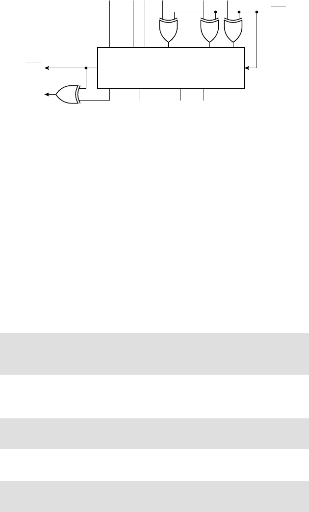
128 CHAPTER THREE numeric basics
y
0
y
1
y
n–1
y
0
c
0
c
n
y
1
y
n–1
…
…
…
…
x
0
x
1
x
n–1
x
0
x
1
x
n–1
… s
0
s
1
s
n–1
s
n–1
/d
n–1
s
1
/d
1
s
0
/d
0
…
c
n–1
adder
add/sub
unsigned
ovf/und
signed
ovf
FIGURE 3.18 An adder/
subtracter for both unsigned and
2s-complement numbers.
This suggests that we can use the same adder/subtracter, shown in
Figure 3.9, that we described for unsigned numbers. The revised form
that deals with both kinds of numbers, unsigned and 2s-complement, is
shown in Figure 3.18. For signed numbers, when the
__
add /sub control
input is 0, the y operand is passed through the XOR gates unchanged
and the carry in to the adder is 0. When the
__
add /sub input is 1, the y
operand is complemented by the XOR gates, and the carry in is 1. Thus
the circuit subtracts by adding to x the complement of y and 1. Depending
on whether the operands are interpreted as unsigned or signed operands,
we use one or the other of the overflow condition outputs.
In Verilog, we express subtraction of signed values using the operator.
For signed values, if we want to allow for a result that would overflow if rep-
resented as the same number of bits as the operands, we can resize the oper-
and values, as we described for signed addition. Thus, given the declarations
wire signed [11:0] v1, v2;
wire signed [12:0] diff;
we can calculate the 13-bit difference between the two 12-bit values using
the assignment
assign diff = {v1[11], v1} – {v2[11], v2};
or in simplified form, relying on Verilog’s implicit sign extension,
assign diff = v1 – v2;

Again, a Verilog model that represents the difference using the same
number of bits as the operands and that derives the overflow condition is
somewhat more involved. Since x y is the same as x ( y), and the sign
of y is the complement of the sign of y (except when y is zero), we can
work out the overflow condition by examining sign bits in a way similar
to that for addition. We just need to use the logical negation of the sign bit
of y in the overflow expression. Thus, for the declarations
wire signed [7:0] x, y, z;
wire ovf;
we can write the following assignments to derive the required difference
and overflow condition bit:
assign z = x – y;
assign ovf = ~x[7] & y[7] & z[7] | x[7] & ~y[7] & ~z[7];
The case of y being zero is handled correctly by this expression, since in
that case, the result z is the same as x, and so the sign of z is the same as
the sign of x.
A further case to consider is subtraction of two unsigned numbers
to give a signed result, rather than underflowing when the difference is
negative. In order to determine the size to use for the result, we can con-
sider the range of possible result values. Suppose we are subtracting n-bit
unsigned values. The greatest result arises from subtraction of zero from
the greatest unsigned value, giving 2
n
1. The least (most negative) result
arises from subtraction of 2
n
1 from zero, giving 2
n
1. This range is
encompassed by a result with n 1 bits. So the simplest way to express
the subtraction is to zero extend the operands by one bit, treat them as
signed, and then apply the signed subtraction operation. In Verilog, given
8-bit operands and a 9-bit result declared as
wire [7:0] v1, v2;
wire signed [8:0] diff;
we could write the subtraction as
assign diff = $signed({1'b0, v1}) – $signed({1'b0, v2});
3.2 Signed Integers
CHAPTER THREE 129

130 CHAPTER THREE numeric basics
Other Arithmetic Operations on Signed Integers
As part of our examination of unsigned integers, we saw that we could
use simplified forms of adder and subtracter to implement the increment
and decrement operations. The same argument applies to incrementing
and decrementing 2s-complement signed integers. However, we won’t go
into the details here. As with unsigned integers, we can use the operator
in Verilog models to add 1 to a signed value to increment, and use the
operator to subtract 1 to decrement the value.
Comparison of signed integers is also done similarly to comparison
of unsigned integers. The main difference arises from the negative weight
for the sign bit. Hence, instead of using x
n 1
___
y
n 1
to compare the most
significant bits in the comparator for x y, we substitute
___
x
n 1
y
n 1
to
compare the sign bits. This follows, since a nonnegative number, with a
sign bit of 0 is greater than a negative number with a sign bit of 1. We
make the corresponding adjustment in a comparator for x y. The Ver-
ilog comparison operators, , , , and , all work on signed values
in an analogous way to unsigned integers.
Scaling a signed integer by a constant power of 2 is slightly different
for signed integers than for unsigned integers. Multiplying by 2
k
involves
shifting to the left by k positions and appending k bits of 0 to the least
significant end. This is the same logical shift left operation that we say for
unsigned numbers. However, if we need to represent the result in the same
number of bits as the original unscaled number, we must truncate using
the resizing rules for 2s-complement described earlier. Thus, the truncated
bits must all be the same as the original sign bit, and the sign of the result
must also have that same sign. Dividing by 2
k
involves shifting the bits
right by k positions, discarding the k least significant bits and appending
k copies of the original sign bit at the most significant end. This operation
is called an arithmetic shift right. It differs from a logical shift right in the
replication of the sign bit instead of filling with 0 bits. Proof that these
operations correctly implement scaling is left to Exercise 3.54.
In Verilog, we can apply the and operators to signed oper-
ands. The operator, like the operator, performs a logical shift
left, but the operator performs an arithmetic shift right. For exam-
ple, if the signed net or variable s has the value 11110011, representing
the value 13
10
, the Verilog expression
s <<< 2
would yield the value 11001100, representing the value 52
10
. The
expression
s >>> 2
would yield the value 11111100, representing the value 4
10
.
The final operation that we discussed in the context of unsigned
integers was multiplication. Extending the multiplier design that we
described there to deal with 2s-complement signed numbers gets quite
complicated, since we need to deal with sign extension within partial
products. In real designs, signed multipliers are based on transformations
of this basic approach to reduce the amount of circuitry required and to
improve performance. We will not go into detail here, but refer to the
books listed in Section 3.6, Further Reading. In any case, using our design
methodology, we can simply express multiplication in Verilog using the *
operator on signed values and let synthesis CAD tools choose an appro-
priate multiplier circuit to use.
1. What is the difference in representation between unsigned binary
and 2s-complement signed binary?
2. What is the range of values that can be represented using 12-bit
2s-complement signed binary form?
3. Write a Verilog declaration for a net that represents a number in the
range 512 to 511 in 2s-complement signed form.
4. Resize the 2s-complement numbers 01110001 and 11110011 to
12 bits and 6 bits. In each case, does the result correctly represent
the same value as the original?
5. Negate the 2s-complement signed number 11110010.
6. How is a signed adder used to perform signed subtraction?
7. How is a 2s-complement signed number multiplied by 16? How is it
divided by 16?
3.3 FIXED-POINT NUMBERS
While many applications deal with integer data, there is a growing list of
applications that also deal with fractional numeric data. Many such appli-
cations involve digital signal processing, in which time-varying analog
signals are sampled, converted to a digital representation and subject to
numerical operations. For example, most modern audio devices deal with
sampled audio signals and perform operations such as filtering, amplifi-
cation and equalization. The audio samples are approximations to real
numbers within a given range. The circuits representing and operating
upon the samples need to deal with fractional values, that is, values that
lie between integers. In this section, we will introduce the notion of fixed-
point representation of nonintegral values.
3.3.1 CODING FIXED-POINT NUMBERS
Suppose we need to represent numeric values that lie in the range 12.0
to 12.0. Since there are an infinite number of real numbers in that range,
KNOWLEDGE
TEST QUIZ
KNOWLEDGE
TEST QUIZ
3.3 Fixed-Point Numbers CHAPTER THREE 131

132 CHAPTER THREE numeric basics
we cannot represent all of them. Instead, we determine a precision, based
on the requirements of our application, and approximate values with a
multiple of that precision. For example, if our chosen precision is 0.01, we
would round each value to the nearest multiple of 0.01. Thus an original
value of 10.23683 would be approximated with a value of 10.24.
When we write decimal numbers in this way, we are extending the
positional notation that we described for integers in Section 3.1. We use
the decimal point to mark the boundary between digits whose weight is a
nonnegative power of 10 and digits whose weight is a negative power of
ten. For example, the number 10.24
10
is
10.24
10
1 10
1
0 10
0
2 10
1
4 10
2
We can extend this idea to binary, in which the digits are weighted
with powers of 2 and each binary digit (each bit) is 0 or 1. Thus, the
binary number 101.01
2
is
101.01
2
1 2
2
0 2
1
1 2
0
0 2
1
1 2
2
Since we are dealing with nonintegral numbers, we use negative powers of
2 for the fractional part. We refer to the period dividing the binary num-
ber into its integral and fractional parts as the binary point.
When we come to implement nonintegral numbers in digital systems,
the question arises of how to represent the binary point. The fixed-point
representation relies on the position of the binary point being implicit. We
just represent the bits, as we did for integral values, as a vector with one
element per bit position. Thus, the number 101.01
2
could be represented
by the bit vector 10101, with the assumption that the binary point lies
two places from the right.
example 3.18 What number is represented by the fi xed-point binary
number 01100010, assuming the binary point is four places from the right?
solution The number is
0110.0010
2
0 2
3
1 2
2
1 2
1
0 2
0
0 2
1
0 2
2
1 2
3
0 2
4
0 4 2 0 0 0
1
8
0 6.125
10
In general, we write an n-bit unsigned fixed-point number with m
bits before the assumed binary point and f bits after the assumed binary
point, where n m f. The number x represented by the bits x
m 1
, . . . ,
x
0
, x
1
, . . . , x
f
is
x x
m 1
2
m 1
. . .
x
0
2
0
x
1
2
1
. . .
x
f
2
f

The smallest number representable using such a code is 0, with a code
word of all 0 bits. The largest number representable has a code word of
all 1 bits, and represents 2
m
2
f
. In between those bounds, numbers are
represented as multiples of the precision, 2
f
.
Note that a code with no digits before the assumed binary point
is permissible, and indeed, practical. This would correspond to a code
with m 0. In such a code, all of the bits represent the fractional part
of the number, so the range is between 0 and 1 2
f
. We can even go
so far as to have the assumed binary point several positions to the left of
the left-most bit, that is, for m to be negative. For example, a code with
m 3 and f 13 would be a 10-bit code with values ranging from 0 to
2
3
2
13
in steps of 2
13
, or in decimal, from 0 to 0.12487. . . in steps
of 0.000122. . . .
Similarly, we can have a fixed-point code with no digits to the right of
the binary point, that is, with f 0. Numbers represented in such a code
are, in fact, unsigned integers. If we substitute f 0 in the expressions for
the upper bound and precision, we get an upper bound of 2
m
1 and a
precision of 1, as we would expect for integers. Thus, integers are just a
special case of fixed-point representation.
We can also use fixed-point representation for signed fractional num-
bers. We use the same approach as we did for integers, changing the weight
of the most significant digit to be negative. This gives us a 2s-complement
fixed-point signed representation. In this case, the number x represented
with m bits before and f bits after the assumed binary point is
x x
m 1
2
m 1
. . . x
0
2
0
x
1
2
1
. . . x
f
2
f
The range of numbers represented using this form is from 2
m 1
to
2
m 1
2
f
, with a precision of 2
f
. Again, we can have a code with
m being zero or negative. Since the left-most bit in a signed fixed-point
representation is the sign bit, a code that represents values between 1
and just less than 1 has m 1, with the single bit before the binary point
being the sign bit.
example 3.19 What number is represented by the signed fi xed-point
binary number 111101, assuming the binary point is four places from the right?
solution The number is
11.1101
2
1 2
1
1 2
0
1 2
1
1 2
2
0 2
3
1 2
4
2 1
1
2
1
4
0
1
16
0.1875
10
Having described how we can represent fixed-point numbers with
a given range and precision, the question arises of determining what
3.3 Fixed-Point Numbers CHAPTER THREE 133

134 CHAPTER THREE numeric basics
range and precision to use in a given application. The answer is not
simple, and depends on the application. In digital signal processing
applications, where fixed-point numbers are used to represent samples
of analog signals, the range of the representation affects the dynamic
range (the ratio of maximum to minimum amplitude) of signals that
can be processed, and the precision affects the signal-to-noise ratio (a
measure of quality or fidelity) of the system. If the system is to per-
form arithmetic operations on the fixed-point values to implement
some processing algorithm, the precision affects the numerical behavior
of the algorithm. The finite precision of the representation means that
analog signal values are only represented approximately, thus, there
is an inherent error in the representation. Some numerical processing
steps can magnify the effect of the error. Also, processing steps might
yield intermediate values whose range differs from that of the samples,
requiring a greater range, and thus more bits, for their representation.
Mathematical analysis of the behavior and sensitivity of numerical
computations is beyond the scope of this book. Nonetheless, it is a vital
early design step in applications that implement numerical processing
procedures. More information is provided in the reference books cited
in Section 3.6, Further Reading.
Fixed-Point Representation in Verilog
We can represent fixed-point numbers in Verilog using vectors. When we
use vectors for integers, we have consistently declared them with index
values corresponding to the binary weights. We can follow the same con-
vention when declaring vectors representing fixed-point numbers. We
specify the left and right index bounds, indicating the power of two for
the weights of the most-significant and least-significant bits, respectively.
We assume that the binary point is between indices 0 and 1, whether
those indices actually occur in a given vector or not.
example 3.20 Write Verilog module declarations for a code converter
that has an input representing an unsigned number in the range 0 to 48 with
a precision of at least 0.01, and an output representing a signed number in the
range 100 to 100 with a precision of at least 0.01.
solution For the input, we need 6 bits before the binary point,
since élog
2
48ù 6. We need a precision that is smaller than 0.01. Since
log
2
0.016.64, we need 7 bits after the binary point. For the output,
élog
2
100ù 7, so we need 7 bits, plus one for the sign bit, giving 8 bits before
the binary point. We just need to extend the 6 pre-binary-point input bits with
two zero bits to get the 8 pre-binary-point output bits. Since we need the same
output precision as the input, we use the same number of bits after the binary
point, namely, 7. The module definition is

module fixed_converter ( input [5:–7] in,
output signed [7:–7] out );
assign out = {2'b0, in};
endmodule
In our discussion of integers, we mentioned that Verilog provides the
type integer for abstract representation of numbers. Unfortunately, Veri-
log does not provide a corresponding type for abstract representation of
fixed-point numbers. Abstract fixed-point types could, in principle, be
included in the language, as has been done in the Ada programming lan-
guage, for example. While we might hope that abstract fixed-point types
might be included in a future version of Verilog as applications become
more common, for now, we will just make use of the vector types.
For testbenches in Verilog, however, we can make use of a built-in
type real. We can declare a variable (but not a net) to be of this type as
follows:
real x;
Real variables are actually represented using floating-point format,
described in Section 3.4. However, we can use them for nonintegral val-
ues to be applied to the inputs or checked at the outputs of models using
fixed-point representation. Some examples are
real r1, r2;
wire [5:-16] x, y;
wire [8:-14] z;
r1 <= $itor(x)/2**16;
r2 <= r1 / ($itor(y)/2**16);
z <= $rtoi(r2 * 2**14);
The conversion function $itor used here converts from a vector value,
interpreted as an integer, to a real-number value. The scaling is required,
since our actual interpretation of the vector is a fixed-point value. The
conversion function $rtoi works in the reverse direction, from a real-
number value to a vector interpreted as an integer. Again, scaling is
required to take account of our actual interpretation of the vector as a
fixed-point value.
3.3 Fixed-Point Numbers CHAPTER THREE 135
136 CHAPTER THREE numeric basics
3.3.2 OPERATIONS ON FIXED-POINT NUMBERS
We now turn to implementation of arithmetic operations on fixed-point
numbers. We have already covered most of what we need in our discus-
sion of arithmetic operations on integers, since fixed-point numbers can
be viewed as scaled integers. For example, if x and y are fixed-point num-
bers with the binary point f positions from the right, then x 2
f
and y 2
f
are integers represented by the same bit vectors as x and y, respectively.
Furthermore,
x y ( x 2
f
y 2
f
)/2
f
We know how to add the two integers, and dividing by 2
f
simply consists
of moving the binary point f places to the left, giving us the result in the
same fixed-point format as x and y. Thus, we can use the same kinds of
adder circuits for fixed-point numbers as for integers. Similar arguments
hold for subtraction, incrementing, decrementing, scaling by constant
powers of 2, and resizing.
One issue we need to be aware of is that a design might represent dif-
ferent signals as fixed-point numbers of different lengths or with the binary
point in different positions. When we perform operations such as addition
or subtraction, we need to ensure that we add or subtract the bits with
corresponding binary weights, wherever they occur in a vector. We may
need to resize one operand to align it with the other. If we need to add or
truncate on the left-hand end of a fixed-point number, the same consider-
ations apply for resizing integers. Thus, in the case of unsigned fixed-point
numbers, we add 0 bits to the left to extend the number, and we truncate
0 bits to reduce its size. In the case of 2s-complement signed numbers, we
replicate the sign bit to extend the number, and we truncate bits to reduce
the number, provided the truncated bits and the resulting sign bit are all
the same as the original sign bit. If we need to add or truncate on the right-
hand end of a number, things are simpler, since the right-most bits all have
positive weight. For both unsigned and 2s-complement representations,
we add 0 bits to extend and truncate bits to reduce the size.
example 3.21 Show how to use an adder for two signed fi xed-point
signals: a, with 4 pre-binary-point and 7 post-binary-point bits, and b, with
6 pre-binary-point and 4 post-binary-point bits. The result c should have
6 pre-binary-point and 4 post-binary-point bits.
solution The operand a needs to be sign extended by two bits on the
left-hand end and can be truncated by three bits on the right-hand end. A 10-bit
adder is needed, connected as shown in Figure 3.19.
Unfortunately, the Verilog and operators applied to vector oper-
ands representing fixed-point numbers do not take care of alignment. They
x
0
10-bit
adder
…
…
a
–4
a
–5
a
–6
a
–7
x
7
a
3
x
8
x
9
y
0
…
…
b
–4
y
7
b
3
b
4
b
5
c
–4
c
3
c
4
c
5
…
y
8
y
9
s
0
…
s
7
s
8
s
9
FIGURE 3.19 Alignment of
operands for fi xed-point addition.

just perform the operations assuming the right-most bits of the operands
are the corresponding least significant bits. If both operands are declared
with the same index bounds, the operations are performed correctly for
the fixed-point interpretation of the values. If, however, the index bounds
are not the same, we need to extend or truncate both ends of the operands
to make sure that the assumed binary points align.
example 3.22 Write Verilog declarations and an assignment to perform
the addition described in Example 3.21.
solution The declarations for the nets a, b and c are
wire signed [3:-7] a;
wire signed [5:-4] b, c;
We could try the following assignment as a first attempt:
assign c = a + b;
Since a is 11 bits and b is 10 bits, the operator would sign extend b to 11 bits
and perform an 11-bit addition. The implicit binary points would be misaligned
by three places. To correct this, we need to sign extend the value of
a by 2
bits, and to truncate the 3 least signficant bits of
a. We can use a part select to
perform the truncation, but the result of a part select is treated as unsigned in
Verilog. We can use the
$signed conversion operation to re-interpret it as signed.
The following assignment incorporates these corrections:
assign c = {{2{a[3]}}, $signed(a[3:–4])} + b;
Another related issue to be aware of is the position of the binary point
in the result of a multiplication. We can appeal to the way in which we
do multiplication of decimals for an analogy. Suppose, for example, that
we wish to multiply 23.76 by 3.128. We first multiply the digits without
regard to the decimal points to get 7432128. We then add the number of
post-decimal digits in the operands, namely, 2 and 3, to get the number of
post-decimal digits in the result, namely, 5. Thus the product is 74.32128.
By analogy, multiplying two fixed-point binary numbers with m
1
and m
2
pre-binary-point bits and f
1
and f
2
post-binary-point bits, respectively, gives
us a product with m
1
m
2
pre-binary-point bits and f
1
f
2
post-binary-
point bits. For example, multiplying 1.101
2
by 10.1
2
gives 100.0001
2
. If
3.3 Fixed-Point Numbers CHAPTER THREE 137
138 CHAPTER THREE numeric basics
we are to use the Verilog * operator to produce a product of this length, we
must extend each operand on the left to the final product size.
1. How is a nonnegative number x represented as a sum of powers of
2 in fi xed-point form?
2. What range of values can be represented as signed fi xed-point
numbers with m pre-binary-point bits and f post-binary-point bits?
3. Write a Verilog declaration for a net x, not to represent numbers in
the range 0.0 to 359.9 with a precision of 0.1.
4. Write a Verilog assignment to subtract the value of a net s2 from the
value of a net s1, where both are of type wire [7:–7], to get a result
net s3 of the same type. No overfl ow detection is required.
5. How many bits are required for the product of two fi xed-point
numbers with 5 pre-binary-point bits and 9 post-binary-point bits?
3.4 FLOATING-POINT NUMBERS
The final number representation that we will discuss in this chapter is
floating-point, which is another representation for approximating real
numbers. They allow for representation of a greater range of numbers
than a fixed-point representation with the same number of bits. However,
implementation of arithmetic operations is considerably more complex.
Indeed, most circuits for floating-point arithmetic are not combinational,
since they would otherwise be too complex and reduce overall system per-
formance. Since we have deferred detailed discussion of sequential circuit
design to a later chapter, we will not go into circuits for floating-point
arithmetic here. For completeness of our survey of numeric representa-
tions in this chapter, we will just introduce floating-point format. Unfor-
tunately, Verilog only provides rudimentary features for dealing with
floating-point numbers. They are not sufficient for modeling floating-
point circuits, so we will not discuss them here.
3.4.1 CODING FLOATING-POINT NUMBERS
Floating-point representation in digital systems is based on the same ideas
as scientific notation for decimal numbers. We can write numbers that are
very small or very large as the product of a fixed-point decimal fraction and
a power of 10. This saves us from writing long strings of leading or trailing
zeros and makes the number much easier to read and understand. Exam-
ples of numbers expressed in scientific notation are 6.02214199 10
23
(Avogadro’s number) and 1.60217653 10
19
(the charge, in Coulombs,
of an electron). We call the fractional part before the sign the mantissa
and the power to which 10 is raised the exponent.
KNOWLEDGE
TEST QUIZ
KNOWLEDGE
TEST QUIZ

Floating-point representations adopt these ideas, but use binary instead
of decimal. The mantissa is expressed as a fixed-point binary number, the
base of the exponent is 2, and the exponent is a signed binary number.
Within these general guidelines, there are many alternative floating-point
representations, and, historically, several have been implemented in com-
puter designs. However, modern general-purpose computers have almost
universally adopted a floating-point representation standardized as IEEE
Standard 754, the so called IEEE floating-point format. In this section,
we will describe this format and formats that differ from it only in the
number of bits used for the mantissa and exponent.
A floating-point number is represented as a vector of bits arranged
as shown in Figure 3.20. The mantissa is represented using a sign bit, s,
located in the left-most bit of the vector, and the unsigned magnitude,
located in the right-most m bits of the vector. The exponent is repre-
sented using e bits between the sign bit and the mantissa magnitude. The
IEEE floating-point standard defines two standard floating-point sizes:
32-bit single precision, with m 23 bits and e 8 bits; and 64-bit double
precision, with m 52 bits and e 11 bits. These are implemented by
most computers. However, if we are designing custom digital circuits for
specific applications, we need not be constrained to these sizes. We can
choose smaller or larger sizes in order to meet the requirements and con-
straints of the application. After we’ve explored some more of the details
of the way in which numbers are represented, we will see how the sizes
of the exponent and mantissa affect the range and precision of numbers
represented.
A floating-point number is usually normalized, meaning that the
magnitude of the mantissa is greater than or equal to 1.0
10
(that is, 1.0
2
)
and less than 2.0
10
(that is, less than or equal to, 1.111. . .1
2
), with the
exponent being adjusted to give the required value for the number. The
mantissa magnitude could be represented as a fixed-point fraction with
the binary point located just to the right of the most significant bit. How-
ever, as a consequence of normalizing, the most significant bit is always 1.
So we can gain an extra bit of precision by not explicitly representing
the most significant bit, but assuming that it is 1. This implicit bit in the
floating-point format is called the hidden bit. Note that the mantissa is
not represented using 2s-complement encoding, even though it is a signed
value. The sign/magnitude representation turns out to have several advan-
tages, including simplification of circuits for some arithmetic operations.
We won’t go into details here.
Similarly, though the exponent is a signed number, it also is not
represented in 2s-complement form. Rather, it is represented in excess
form. That is, for a given actual exponent value E, we represent it with the
e-bit unsigned binary code for E 2
e 1
1. The value 2
e 1
1 is called
the bias, and is chosen so that a symmetric range of positive and nega-
tive actual exponent values can be represented. For example, if 5 bits are
s
e bits m bits
exp mantissa
FIGURE 3.20 Floating-point
format.
3.4 Floating-Point Numbers
CHAPTER THREE 139
used for the exponent, the bias would be 2
4
1 15, that is, 01111
2
. An
actual exponent value of 3 would be represented using the 5-bit unsigned
binary code for 3 15 18, that is 10010
2
. The reason for using excess
coding is that all exponent codes are unsigned. Given the position of the
exponent within a floating-point code word, and the fact that numbers
with smaller exponents are smaller than numbers with larger exponents
(due to normalization), floating-point numbers can be compared using
the same hardware as for comparing integers. This is a useful trick for
saving cost and execution time in floating-point arithmetic hardware.
Let’s now consider the range and precision of values that can be
represented using floating-point format. As with fixed-point numbers,
the range and precision are important factors that influence the numeri-
cal behavior of computations. The range of values is determined by the
length of the exponent, since the most positive exponent determines the
largest value and the most negative exponent determines the smallest
value. The IEEE floating-point format reserves two exponent encodings
for special purposes: the largest encoding, 2
e
1, with all 1 bits; and the
smallest encoding, with all 0 bits. We will return to these shortly. Setting
them aside, the smallest exponent has an encoding of 1, representing an
actual exponent value of 2
e 1
2. Putting this together with the smallest
mantissa magnitude of 1.0 gives us the smallest representable value of
1.0 2
2
e 1
2
. The largest exponent has an encoding of 2
e
2, repre-
senting an actual exponent value of 2
e 1
1. Putting this together with
the largest mantissa magnitude of just under 2.0 gives us the largest rep-
resentable value of just under 2.0 2
2
e 1
1
, that is, 2
2
e 1
. For IEEE
single-precision format, this corresponds to a range of approximately
1.2 10
38
to 3.4 10
38
, and for IEEE double-precision format,
a range of approximately 2.2 10
308
to 1.8 10
308
. A custom
floating-point representation with a 5-bit exponent, on the other hand,
would give us a range of approximately 6.1 10
5
to 6.6 10
4
.
When considering the precision of floating-point numbers, we usually
talk about relative precision, since absolute precision varies with the
exponent. The relative precision is determined by the number of bits in
the mantissa magnitude. All of the bits are significant, since there are
no leading zeros in the mantissa (taking into account the hidden bit). So
the relative precision remains the same across the full range of values,
and is approximately 2
m
. Another way of thinking about precision is to
specify the number of significant decimal digits, which is approximately
m log
10
2, that is m 0.3 digits. For example, IEEE single-precision for-
mat gives a precision of approximately 7 decimal digits, and IEEE double-
precision format gives approximately 16 decimal digits. A custom format
with 16 bits of mantissa magnitude would give a precision of approxi-
mately 5 decimal digits.
140
CHAPTER THREE numeric basics
We can return now to the special exponent encodings that we mentioned
above. First, the smallest exponent encoding, all zeros, is used for denormal
numbers, in which the hidden bit is 0. The actual exponent is still repre-
sented using excess form, and so has a value of 2
e 1
1. Thus, denormal
numbers are all smaller in magnitude than the smallest normalized number,
though they have fewer significant bits. They allow for gradual under-
flow in a computation, where the results diminish toward 0.0 once the
limit of precision has been reached. This feature of the representation
improves the numerical behavior of some algorithms. If all the mantissa
bits in a denormal number are 0, we get 0.0 2
2
e 1
1
. Thus, there
are two alternate representations for 0.0, one with a sign bit of 0 and the
other with a sign bit of 1. The IEEE standard specifies that a zero result
in most cases be represented by the nonnegative version, but that in any
case, the two versions should be deemed equal.
The other special exponent encoding, all 1s, has two uses. If the man-
tissa magnitude bits are all 0 (not counting the hidden bit), the number
represents an infinite value. The value of the sign bit determines whether
it is a positive or negative infinity. Operations that overflow generally
yield an infinite result, which is maintained in subsequent computations.
This avoids having to check for overflow until completion of a multistep
computation, thus improving performance. If the exponent encoding is
all 1s and the mantissa magnitude is other than all 0s, the value is said
to represent not a number (NaN). NaN results arise from computations
such as division of 0 by 0, and can also be maintained through a multistep
computation.
In addition to the representation for floating-point numbers, the IEEE
standard also specifies how arithmetic operations are to be performed,
provides options for specifying how operations are to be rounded, and
specifies the conditions under which exceptions may occur. (A system may
abort a computation or take recovery action when an exception occurs.)
The details are beyond the scope of this book, but can be found in the
Further Reading references.
For a given number of bits of representation, floating-point representa-
tion can give a larger range of values than fixed-point, albeit at the expense
of precision. The choice between floating-point and fixed-point in a given
application will depend largely on the range of values that must be repre-
sented, both for the input and output signals, as well as for intermediate
results during computation. There is also a trade-off with the complexity of
circuits needed to perform the computations. Fixed-point circuits are gen-
erally simpler, but if significantly more bits are needed to get the required
range, the circuits may consume more area. In many cases, the choice will
only be made after thorough exploration of the numerical behavior of
the computations to be performed and comparison of implementation
3.4 Floating-Point Numbers CHAPTER THREE 141
142 CHAPTER THREE numeric basics
complexities of alternate representations. This exploration will usually be
performed by a system architect early in the development process. The
result of the exploration will be a design specification that includes details
of number representations to be used within the system. In a circuit that
is customized for a particular application, a floating-point representation
can use exponent and mantissa sizes other than those defined by the IEEE
standard, thus reducing cost and potentially improving performance.
1. Express the number 4.5
10
in fl oating-point format with 5 bits of
exponent and 12 bits of mantissa magnitude.
2. What values are represented by the following bit vectors, interpreted
in fl oating-point format with 4 bits of exponent and 11 bits of
mantissa magnitude: 0000000000000000, 0111100000000000 and
0100010000000000?
3. Determine the minimum number of exponent and mantissa bits
required to represent a fl oating-point value in the range 100 to
100 with a precision of at least 4 decimal digits.
KNOWLEDGE
TEST QUIZ
KNOWLEDGE
TEST QUIZ

3.5 CHAPTER SUMMARY
A nonnegative integer x less than or equal to 2
n
1 is represented in
n-bit unsigned binary form as
x x
n 1
2
n 1
x
n 2
2
n 2
. . .
x
0
2
0
A signed integer x between 2
n 1
and 2
n 1
1 inclusive is repre-
sented in n-bit 2s-complement form as
x x
n 1
2
n 1
x
n 2
2
n 2
. . .
x
0
2
0
Octal (base 8) and hexadecimal (base 16) are shorthand codes for
binary codes.
Unsigned and signed integers are modeled in Verilog using vector
values, or using the type
integer. For signed integers the keyword
signed is used in the net or variable declaration. Arithmetic opera-
tors can be used for these types.
An unsigned number is zero-extended by adding 0s to the left, and is
truncated by discarding leading 0s. A 2s-complement signed number
is sign-extended by replicating the sign bit to the left, and is trun-
cated by discarding leading copies of the sign bit.
Addition of binary-coded integers is performed by an adder circuit.
The simplest form of adder is a ripple-carry adder. Fast carry chain,
carry-lookahead and other adder structures improve performance at
the cost of circuit area and power.
A 2s-complement signed integer is negated by complementing and
adding 1.
Subtraction of binary-coded integers can be implemented using an
adder by complementing the second operand and setting the carry in
to 1.
A magnitude comparator compares two binary-coded integers for
equality or inequality (greater than or less than comparison).
Binary-coded integers are multiplied by a power of two by a logical
shift left. Unsigned integers are divided by a power of 2 by a logical
shift right. 2s-complement signed integers are divided by a power of
2 by an arithmetic shift right.
A combinational multiplier forms partial products by multiplying
one operand by each bit of the other operand, then adds the partial
products to form the product.
왘
왘
왘
왘
왘
왘
왘
왘
왘
왘
왘
3.5 Chapter Summary CHAPTER THREE 143

144 CHAPTER THREE numeric basics
Gray codes change only in one bit position between adjacent
|code words. They are commonly used in electromechanical
position sensors.
A fractional number can be represented in fixed-point binary form
by assuming a fixed position for the binary point. Arithmetic circuits
for integers can be used, since fixed-point numbers can be inter-
preted as scaled integers.
Fixed-point numbers are modeled in Verilog using vector values.
Arithmetic operators can be used for these types, provided the
implicit binary points are properly aligned.
A fractional number can be represented in floating-point binary form
with a signed mantissa and an exponent. IEEE format specifies sign/
magnitude representation for the mantissa and excess representation
for the exponent. Special representations are provided for denormal
numbers, infinities and not-a-number values.
Modeling a design using vector types and arithmetic operations allows
a synthesis tool to choose arithmetic components optimized for the
target fabric, subject to performance requirements and constraints.
3.6 FURTHER READING
Digital Arithmetic, Miloš D. Ercegovac and Tomás Lang, Morgan
Kaufmann Publishers, 2004. A comprehensive reference on numeri-
cal representations and algorithms and circuit structures for arith-
metic operations.
Understanding Digital Signal Processing, Richard G. Lyons, Prentice
Hall, 2001. An introduction to the theory of digital signal process-
ing (DSP), including a discussion of the effects of finite fixed-point
representation.
IEEE Standard for Binary Floating-Point Arithmetic, IEEE Std 754-
1985. This standard defined the representation for single- precision
(32-bit) and double-precision (64-bit) and extended-precision
floating-point numbers. It also specifies how arithmetic operations
on such numbers are to be performed.
exercise 3.1
Express the following decimal numbers in 8-bit unsigned
binary form: 5, 83 and 240.
exercise 3.2 What decimal numbers are represented by the following
8-bit unsigned binary numbers: 00100101 and 11000000?
왘
왘
왘
왘
왘
EXERCISESEXERCISES

exercise 3.3 What range of numbers can be represented in unsigned
binary form in 6 bits, in 14 bits and in 30 bits?
exercise 3.4 How many bits are required to represent numbers in each
of the following ranges in unsigned binary form: 0 to 31, 0 to 100, 0 to 1000
and 0 to 8191?
exercise 3.5 How many bits would be required to represent:
a) An angle in degrees between 0˚ and 360˚.
b) The milage on a car odometer, assuming six decimal digits.
c) The delay in a radar echo in ns, assuming a maximum delay of 1ms.
exercise 3.6 Express the following unsigned binary numbers in octal:
001110010, 00000000 and 1111011111.
exercise 3.7 Express the following unsigned binary numbers in hexadeci-
mal: 10000101, 01111101, 1111001001 and 000011111.
exercise 3.8 What numbers, expressed in unsigned binary form, are
represented by the following octal numbers: 7024 and 0001?
exercise 3.9 What numbers, expressed in 8-bit unsigned binary form,
are represented by the following octal numbers: 055 and 307?
exercise 3.10 Is 2901 a valid octal number? If so, what unsigned binary
number does it represent? If not, why not?
exercise 3.11 What numbers, expressed in unsigned binary form, are
represented by the following hexadecimal numbers: 7F39BA, C108 and 7024?
exercise 3.12 What numbers, expressed in 10-bit unsigned binary form,
are represented by the following hexadecimal numbers: 06C and 307?
exercise 3.13 Is 2GA1 a valid hexadecimal number? If so, what
unsigned binary number does it represent? If not, why not?
exercise 3.14 Resize the following unsigned binary numbers to 8 bits:
01101, 111000, 0001011001, 0011110000 and 000110001001. In which cases
does the result not represent the same numeric value as the original number?
Exercises CHAPTER THREE 145

146 CHAPTER THREE numeric basics
exercise 3.15 Perform the following unsigned binary additions. In each
case, can the result be represented in the same number of bits as the operands, or
is an extra bit required?
a) 01011001 01011110
b) 11110001 01110100
c) 10000010 11000001
exercise 3.16 Perform the following unsigned binary additions to
produce 8-bit results. In each case does the addition overflow or not?
a) 00111000 10010000
b) 11110000 00010010
c) 11111100 10000111
exercise 3.17 Draw circuits composed of gates that implement a half
adder and a full adder.
exercise 3.18 Identify two unsigned binary numbers for which a
ripple-carry adder exhibits its worst-case delay. Show how the propagation of
signals through the components of the adder cause the delay to be the worst-
case delay.
exercise 3.19 For the addition of the two 14-bit unsigned binary num-
bers 01110001010101 and 11100011000110, with c
0
= 1, determine the values
of k
i
, p
i
and g
i
for each bit position
i
, and thus determine the values of s
i
and
c
i +1
. What is the longest chain of propagated carries in this addition?
exercise 3.20 Draw a circuit composed of gates that implements the
4-bit-wide carry-lookahead generator shown in Figure 3.7.
exercise 3.21 We have shown that addition of two n-bit unsigned binary
numbers requires n 1 bits for the result to be represented without overflow.
Show that addition of three n-bit unsigned binary numbers also requires no more
than n 1 bits.
exercise 3.22 Write a Verilog model of a circuit that adds three 12-bit
unsigned binary numbers to produce a 13-bit result with no overflow detection.
exercise 3.23 Develop a Verilog testbench model for the adder described
in Exercise 3.22.
exercise 3.24 Write a Verilog model of a circuit that adds three 12-bit
unsigned binary numbers to produce a 12-bit result with overflow detection.

exercise 3.25 Develop a Verilog testbench model for the adder described
in Exercise 3.24.
exercise 3.26 Perform the following unsigned binary subtractions to
produce 8-bit results. In each case does the subtraction underflow or not?
a) 10111000 01010000
b) 01110000 00110010
c) 01111100 10000111
exercise 3.27 Prove Equations 3.11 and 3.12.
exercise 3.28 Determine the Boolean equations for an unsigned decre-
menter by simplifying Equations 3.11 and 3.12 for an unsigned subtracter.
exercise 3.29 Revise the equality comparator of Figure 3.11, for 16-bit
x and y inputs, by replacing the n-input AND gate with two-input NAND and
NOR gates. Hint: DeMorgan’s law tells us that
___
a b
_
a
_
b.
exercise 3.30 The magnitude comparator of Figure 3.12 suffers from
similar worst-case delay behavior to that of a ripple-carry adder. The final result
may require the result of comparison of the least significant bits to ripple up the
chain of AND and OR gates. Devise a 4-bit lookahead magnitude comparator
that avoids the ripple behavior.
exercise 3.31 Perform a logical shift left by 4 positions on each of
the following unsigned numbers to form a 12-bit result: 000111000110 and
000010110100. In each case, does an overflow occur?
exercise 3.32 Perform a logical shift right by 4 positions on each of
the following unsigned numbers to form a 12-bit result: 100101010000 and
000101001000. In each case, does the result exactly represent division by 16?
exercise 3.33 Perform the following unsigned binary multiplication to
form a 12-bit result: 101001 010101.
exercise 3.34 Suppose we use a 4-bit unsigned binary representation to
encode the rotational position of the shaft in Figure 3.14 instead of a Gray code.
Identify all cases where more than one bit changes between adjacent code words.
exercise 3.35 Devise a 5-bit Gray code using the scheme described in
Section 3.1.3.
exercise 3.36 Develop a Verilog model of a converter that converts
from a 4-bit unsigned binary code input to a 4-bit Gray coded output.
Exercises CHAPTER THREE 147

148 CHAPTER THREE numeric basics
exercise 3.37 Express the following decimal numbers in 8-bit
2s-complement signed form: 5, 83 and 120.
exercise 3.38 What decimal numbers are represented by the following
8-bit 2s-complement signed numbers: 00100101 and 11000000?
exercise 3.39 What range of numbers can be represented in
2s-complement signed form in 6 bits, in 14 bits and in 30 bits?
exercise 3.40 How many bits are required to represent numbers in each
of the following ranges in 2s-complement signed form: 32 to 31, 100 to 100,
1000 to 1000 and 8192 to 8191?
exercise 3.41 How many bits would be required to represent:
a) A temperature in ˚C between absolute zero (273˚C) and 5000˚C.
b) An altitude in meters, between 5000 (below sea level) and 20,000 (above
sea level).
exercise 3.42 Resize the following 2s-complement signed numbers to 8
bits: 01101, 111000, 0001011001, 0011110000 and 111110001001. In which
cases does the result not represent the same numeric value as the original number?
exercise 3.43 Negate the following 2s-complement signed numbers:
00111010, 11101111 and 00000000.
exercise 3.44 Perform the following 2s-complement signed additions to
produce 8-bit results. In each case, can the result be represented correctly in the
same number of bits as the operands?
a) 01011001 01011110
b) 11110001 01110100
c) 11111100 11110010
d) 10000010 11000001
exercise 3.45 Write a Verilog model of a circuit that adds three
12-bit 2s-complement signed numbers to produce a 12-bit result with overflow
detection.
exercise 3.46 Develop a Verilog testbench model for the adder described
in Exercise 3.45.
exercise 3.47 Perform the following 2s-complement signed subtractions
to produce 8-bit results. In each case does the subtraction overflow?

a) 10111000 01010000
b) 01110000 00110010
c) 01111100 10000111
d) 11110001 10001010
exercise 3.48 Show how a 2s-complement adder/subtractor can be used
to compute the absolute value of number. Hint: y 0 y and y 0 y.
exercise 3.49 Draw a circuit composed of gates, similar to that of
Figure 3.12, that implements a 2s-complement signed magnitude comparator.
exercise 3.50 Perform a logical shift left by 4 positions on each
of the following 2s-complement signed numbers to form a 12-bit result:
000111000110, 111111100101 and 000000110100. In each case, does an
overflow occur?
exercise 3.51 Perform an arithmetic shift right by 4 positions on
each of the following 2s-complement signed numbers to form a 12-bit result:
100101010000 and 000101001000. In each case, does the result exactly repre-
sent division by 16?
exercise 3.52 Write a Verilog model of a circuit that calculates the
average of four 16-bit 2s-complement signed numbers, without checking for
overflow. Hint: use a shift operation to perform the division by 4.
exercise 3.53 Develop a Verilog testbench model for the averager
described in Exercise 3.52.
exercise 3.54 Prove that the shift-left and arithmetic shift-right opera-
tions described in Section 3.2.2 correctly implement scaling by a power of 2.
exercise 3.55 What numbers are represented by the following unsigned
fixed-point binary numbers, assuming the binary point is three places from the
right: 1001001 and 0011110?
exercise 3.56 What is the range and precision of each of the following
unsigned fixed-point representations, with m pre-binary-point and f post-binary-
point bits:
a) 12 bits, with m 5 and f 7
b) 10 bits, with m 2 and f 12
c) 8 bits, with m 12 and f 4
Exercises CHAPTER THREE 149

150 CHAPTER THREE numeric basics
exercise 3.57 How many pre-binary-point and post-binary-point bits
would be required to represent numbers in the range 0.0 to 12.0 with a precision
of 0.003?
exercise 3.58 What numbers are represented by the following signed
2s-complement fixed-point numbers, assuming the binary point is four places
from the right: 00101100 and 11111101?
exercise 3.59 What is the range and precision of each of the following
signed 2s-complement fixed-point representations, with m pre-binary-point and
f post-binary-point bits:
a) 14 bits, with m 6 and f 8
b) 8 bits, with m 4 and f 12
exercise 3.60 How many pre-binary-point and post-binary-point bits
would be required to represent numbers in the range 5.0 to 5.0 with a preci-
sion of 0.02?
exercise 3.61 Write a Verilog entity declaration for a component that
calculates the square of a signed fixed-point number with 4 pre-binary-point and
6 post-binary-point bits. The result is unsigned, with 8 pre-binary-point
and 6 post-binary-point bits.
exercise 3.62 Show how a 16-bit signed integer adder/subtracter can be
used to add two signed operands, a, with 3 pre-binary-point and 9 post-binary-
point bits, and b, with 7 pre-binary-point and 5 post-binary-point bits, to produce
a result with 7 pre-binary-point and 9 post-binary-point bits and no carry or
overflow outputs.
exercise 3.63 Given a floating-point representation with 7 exponent bits
and 16 mantissa bits:
a) How would the following numbers be represented: 5.625 and 0.3125?
b) What values are represented by the following floating point numbers,
shown in hexadecimal shorthand: 44F000 and BC4000?
c) What is the range and precision of the floating-point representation?
exercise 3.64 Determine the smallest floating-point representation that
includes values whose absolute value is in the range 10
6
to 10
6
and that has a
precision of 6 decimal digits.
sequential basics
Sequential circuits are the mainstay of digital systems. In this chapter,
we start by examining several sequential circuit elements that are widely
used in digital systems for storing information and for counting events.
We then see how a system can be built from two main sections: a data-
path and a control section. We complete the chapter with a discussion of
a clocked synchronous timing methodology based on the abstraction of
discrete time. This methodology is central to design of complex digital
systems.
4.1 STORAGE ELEMENTS
In Chapter 1, we briefly introduced the idea of sequential circuits. We
described a sequential circuit as one whose outputs depend not only on
the current values of inputs, but also on the previous values of inputs.
Such circuits have some form of memory, or storage, of the history of
input values. We mentioned that sequential circuits are commonly regu-
lated by a periodic clock signal that divides the passage of time into dis-
crete clock cycles. We also showed one of the simplest elements for storing
values, a D flip-flop, that can store one bit of information. In this section,
we will look at further uses of the D flip-flop and other storage elements.
4.1.1 FLIP-FLOPS AND REGISTERS
As a reminder, the symbol for a D flip-flop is shown in Figure 4.1, and
a timing diagram is shown in Figure 4.2. The flip-flop is edge-triggered,
meaning that on each rising edge of the clk input, the current value of the
D input is stored within the flip-flop and reflected on the Q output. We
illustrated use of D flip-flops in sequential circuits in Example 1.2, where
we stored the previous two values of an input signal on successive clock
edges so that we could detect a given sequence of input values.
While it is possible to implement a flip-flop as a combination of gates,
it is not very instructive to do so. Moreover, flip-flops are provided as
DQ
clk
FIGURE 4.1 A D fl ip-fl op.
151
4
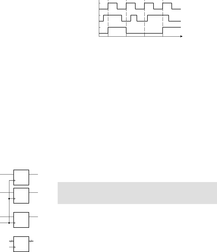
primitive elements in most implementation fabrics, so we would only need
to implement one using gates in very exceptional circumstances. Advanced
books on IC design typically include more detailed treatment of flip-flop
implementation (see Section 4.6, Further Reading).
In most digital circuits, flip-flops are not used individually, but in
groups to store binary-coded values. A group of flip-flops used in this
way is called a register. Each flip-flop in the register stores one bit of the
code word of the stored value, as shown in Figure 4.3. The circuit at the
top of the figure shows that each bit of an input and an output signal is
connected to the input and output, respectively, of one of the flip-flops,
and that the clock signal is connected in common to the clock input of all
of the flip-flops. When there is a rising edge on the clock input, each flip-
flop in the register updates its stored bit from the signal connected to its
data input and drives the new value on its data output. The symbol for the
register is shown at the bottom of Figure 4.3. The difference, compared
to the symbol for a single flip-flop, is in the thick lines used for the data
input and output, denoting multiple bits. We can think of this as a more
abstract component that has similar behavior to a D flip-flop, except that
it stores a complete code word rather than a single bit.
We can model simple D flip-flops and registers in Verilog using an
always block of the form
always @(posedge clk)
q <= d;
This is the first of a small number of always-block templates that we will
introduce for modeling sequential circuits. It is important that we adhere
to the template structures, since synthesis tools can generally only syn-
thesize sequential circuits that use the templates. A complete description
of the templates and the way synthesis tools process them is included in
Appendix C.
We would place a block representing a flip-flop or register in the
statement part of a module. The notation @(...) after the always keyword
is called the block’s event list, and specifies an event to which the block
responds. In this case, the keyword posedge specifies that the event is a
positive (rising) edge, a change from 0 to 1, on the clock input clk. When
DQ
DQ
DQ
d(0)
…
…
…
d(1)
d(n)
nn
q(0)
q(1)
q(n)
clk
DQ
clk
clk
clk
clk
FIGURE 4.3 A register com-
posed of D fl ip-fl ops (top), and the
symbol for the register (bottom).
152 CHAPTER FOUR sequential basics
D
clk
Q
FIGURE 4.2 Timing diagram
for a D fl ip-fl op.
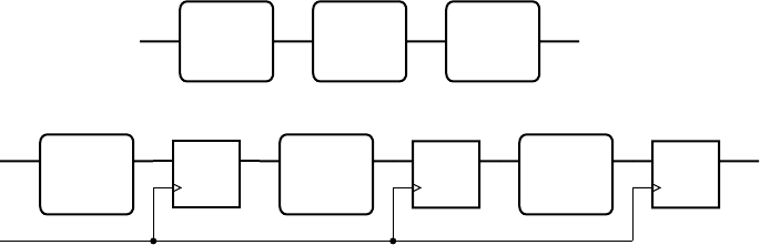
the event occurs, the block performs the statement that follows. (If there is
more than one statement to perform, we can group them using begin . . .
end
keywords.) The statement in this case assigns the current value of the
data input d to the data output q. Since this assignment only happens on
rising edges of clk, and the value of q remains unchanged between rising
edges, the block models the behavior we described for an edge-triggered D
flip-flop or a register. The distinction between the two arises from the sizes
of d and q. If they are single bits, the block models a D flip-flop, storing
just a single bit of data. If d and q are vectors, the block models a register.
There are two further points to note about this model for a flip-flop
or register. First, the output q must be declared as a variable, for example,
using a reg or integer keyword. As we have previously mentioned, assign-
ments within procedural blocks must be made to variables, not nets. Sec-
ond, we have used a different form of assignment symbol, instead of ,
in this block. The form using is called a blocking assignment, and can be
used in blocks that model combinational logic, as we saw in Chapter 2.
The form using is called a nonblocking assignment, and should be
used in assignments to variables representing the outputs of flip-flops or
registers. The reason for the distinctions arise from subtleties in the way
variables are updated during simulation of Verilog models. We will not go
into details in this book. (The details are covered in reference books on
Verilog.) Instead, we will simply follow the convention of using nonblock-
ing assignments in blocks modeling outputs of sequential logic.
One use for a register constructed from simple D flip-flops is as a
pipeline register in a sequential design. We will discuss this in further
detail in Chapter 9, focusing on the use of pipelining as a technique for
improving performance of a digital system. For now, consider the circuit
outlined at the top of Figure 4.4. Successive values of data arriving at
the input are processed by a number of combinational subcircuits, for
example, by arithmetic subcircuits built from components described in
Chapter 3. The total propagation delay of the circuit is the sum of the
propagation delays of the individual subcircuits. This total delay must be
less than the interval between arriving data values, otherwise data values
may be lost. If the total delay is too long, we can divide the circuit into
segments by inserting a register after each subcircuit, as shown at the
4.1 Storage Elements CHAPTER FOUR 153
DQ
combi-
national
circuit 1
DQ
combi-
national
circuit 2
DQ
combi-
national
circuit 3
d_in
clk
d_out
combi-
national
circuit 1
combi-
national
circuit 2
combi-
national
circuit 3
d_in d_out
clk clk clk
FIGURE 4.4 A circuit
composed of combinational
subcircuits (top), and a pipeline
containing the same subcircuits.

bottom of Figure 4.4. This arrangement is called a pipeline, as it allows
data and intermediate results to flow through over several clock cycles.
A new input value arrives at the beginning of each clock cycle. During
a clock cycle, each subcircuit uses the value from the preceding regis-
ter (or from the input, in the case of the first subcircuit) to perform its
combinational function and to yield an intermediate result. On the next
rising clock edge, the intermediate results are stored in the registers at the
outputs of the subcircuits. Each intermediate result is then used by the next
subcircuit during the next clock cycle. Computation is thus performed in
assembly-line fashion. A new final result reaches the output on each clock
edge, having taken several clock cycles to be computed.
example 4.1 Develop a Verilog model for a pipelined circuit that com-
putes the average of corresponding values in three streams of input values,
a, b
and c. The pipeline consists of three stages: the fi rst stage sums values of a and
b and saves the value of c; the second stage adds on the saved value of c; and
the third stage divides by three. The inputs and output are all signed fi xed-point
numbers indexed from 5 down to 8.
solution The module definition is
module average_pipeline ( output reg signed [5:–8] avg,
input signed [5:–8] a, b, c,
input clk );
wire signed [5:–8] a_plus_b, sum, sum_div_3;
reg signed [5:–8] saved_a_plus_b, saved_c, saved_sum;
assign a_plus_b = a + b;
always @(posedge clk) begin // Pipeline register 1
saved_a_plus_b <= a_plus_b;
saved_c <= c;
end
assign sum = saved_a_plus_b + saved_c;
always @(posedge clk) // Pipeline register 2
saved_sum <= sum;
assign sum_div_3 = saved_sum * 14'b00000001010101;
always @(posedge clk) // Pipeline register 3
avg <= sum_div_3;
endmodule
154 CHAPTER FOUR sequential basics
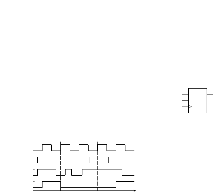
The nets and variables declared within the module are used for the intermediate
results of the arithmetic operations and for the values saved in registers. The sim-
ple assignment statements model the arithmetic operations (two additions and a
multiplication). We express the division by three as a multiplication by one-third
(expressed as the binary fixed-point number 14'b00000001010101), as multipli-
ers are generally simpler circuits than dividers. Moreover, some implementation
fabrics have built-in multipliers that can be used. The three always blocks model
the pipeline regi
sters storing the intermediate results. Note that the first register
actually stores two values together: the sum of
a and b, and the input value c. If
c were not saved in this way, the wrong value from the input stream c would be
added by the second adder, rather than the value corresponding to the saved sum
of
a and b. Also note that the third register assigns directly to the output avg, as
the value saved by the third register is the value required at the output.
The D flip-flop that we have considered so far is somewhat limited
in its use, since it stores a new value on every rising edge of the clock
input. Many systems only require a flip-flop to store a value when some
controlling condition arises. For that, we can use an enhanced form of D
flip-flop with a clock-enable input (sometimes call a load-enable input),
illustrated in Figure 4.5. This flip-flop only updates the stored value when
the
CE input is 1 at the time of a rising clock edge. If the CE input is 0 on a
rising clock edge, the flip-flop maintains the stored value unchanged. This
behavior is shown in the timing diagram in Figure 4.6. As we mentioned
in Section 1.3.6, the value on the data input must be stable for the setup
time before and the hold time after the clock edge. A similar constraint
applies to the clock-enable input. We say that the clock-enable input is a
synchronous control input, meaning that it must be stable around a clock
edge, and its effect is only acted upon when a clock edge occurs.
As with the simple D flip-flop, we can use multiple flip-flops with
clock enable in parallel to form a register with clock enable. This form of
register is probably the most common used in sequential digital systems, as
it allows for storage of an intermediate result computed during one clock
cycle to be used as an input to a subsequent computation any number of
4.1 Storage Elements CHAPTER FOUR 155
D
CE
Q
clk
FIGURE 4.5 A D fl ip-fl op
with clock-enable input.
D
CE
clk
Q
FIGURE 4.6 Timing diagram
for a D fl ip-fl op with clock enable.
clock cycles later. We will see in Section 4.3 how we can develop control
conditions that govern when data is stored in registers.
We can model flip-flops and registers with clock enable inputs by
extending the always-block template used to model simple D flip-flops
and registers. The revised template is
always @(posedge clk)
if (ce) q <= d;
The difference between this and the previous template is the addition of
the if statement. When a rising edge occurs on the clk input, the output
signal is only updated if the ce input is 1; otherwise, the stored value is
unchanged. As before, the sizes of d and q determine whether the block
models a single-bit flip-flop or a multibit register.
A further extension to the simple flip-flop involves adding an input
to reset the stored value to 0. This is useful for ensuring that the flip-flop
is initialized to a known state when power is first applied to a sequential
circuit or when the circuit must be restarted from an initial state. Some
circuits include a push button to allow the user to reset the circuit, for
example, when it has encountered an error condition from which it cannot
recover. Figure 4.7 shows a symbol for a flip-flop with both a clock-enable
input and a reset input. The reset input overrides the clock-enable and
data inputs. That is, when reset is 1, the stored value and the output Q are
both changed to 0, regardless of the values on the CE and D inputs.
An important question to consider is the timing of changes on the
reset input and when the reset operation occurs. There are two alternative
behaviors, and a flip-flop with reset exhibits one or the other. The first
reset behavior is called synchronous reset, and treats the reset input as a
synchronous control input. This behavior is illustrated in Figure 4.8, in
which the reset input causes the flip-flop to be reset on the first, fourth
and fifth rising clock edges. Notice that, during the seventh clock cycle,
reset changes to 1, but then changes back to 0 before a clock edge occurs.
Since reset is 0 at the time of the next clock edge, the flip-flop is not reset.
D
CE
Q
reset
clk
FIGURE 4.7 A D fl ip-fl op
with clock-enable and reset inputs.
D
CE
reset
clk
Q
12345678
FIGURE 4.8 Timing diagram
for a fl ip-fl op with clock-enable
and synchronous reset inputs.
156 CHAPTER FOUR sequential basics
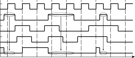
Notice also that we have shown the initial value of the Q output as neither
0 nor 1, but some unknown value, denoted by the grey shading. The fact
that reset is 1 at the first clock edge forces the output to the known 0
value. Finally, we have ensured that the value of reset, like other data and
control inputs is stable around each clock edge.
The second reset behavior for flip-flops is called asynchronous reset.
In this case, the reset input is treated as an asynchronous control input,
that is, when it changes to 1, it has an immediate effect regardless of
the value of the clock or occurrence of clock edges. Moreover, the effect
continues for as long as the reset input is 1. This behavior is illustrated in
Figure 4.9. The timing of the inputs is the same as in Figure 4.8, but the
output timing is different. At the start and in the third cycle, Q changes
to 0 as soon as reset changes to 1, rather than waiting until the next clock
edge. Furthermore, in the seventh cycle, the reset pulse that was ignored
in the previous diagram takes effect in this case.
There is a potential problem that we should be aware of when design-
ing circuits with asynchronous reset. The effect of changing the reset
input from 1 back to 0 is to allow flip-flops to resume normal operation.
However, if the change occurs close to a clock rising edge, the effect may
occur at that edge or be delayed until the subsequent edge. This can cause
problems in a system with numerous flip-flops, all of which are connected
to the same clock and reset signals. Differences in the wiring delays can
cause the change of reset from 1 to 0 to occur at slightly different times
relative to clock edges for different flip-flops. Consequently, some flip-
flops may be released from reset and resume storing values at one clock
edge, whereas others might not resume until the subsequent clock edge,
resulting in incorrect circuit operation. The solution to this problem is
to ensure that the release of the reset signal from 1 to 0 always occurs
synchronously with the clock; that is, to ensure that the change occurs
sufficiently before a clock edge that the reset signal is stable around the
edge for all flip-flops in the system.
4.1 Storage Elements CHAPTER FOUR 157
D
CE
reset
clk
Q
12345678
FIGURE 4.9 Timing diagram
for a fl ip-fl op with clock-enable
and asynchronous reset inputs.

The choice between synchronous and asynchronous reset may be
influenced by the implementation fabric used for a design. Some fabrics
only provide flip-flops with one or the other form of reset. Others, such
as many FPGAs, allow us to program each flip-flop to use one or the
other form of reset. Alternatively, the choice between the two forms of
reset may be made by a system architect based on requirements for the
design or the timing practices adopted for the design project. In that case,
the chosen form of reset would be incorporated as a design specification
for the subcircuits of the larger system. Generally, we should simplify the
timing of a design by adopting one form of reset, either synchronous or
asynchronous, uniformly throughout the design.
Just as we can use simpler flip-flops in parallel to form registers, so we
can use flip-flops with reset in parallel. The result is a register that can be
reset to a code word of all 0s. We can model flip-flops and registers with
reset in Verilog by extending our previous always-block templates. The
template for a flip-flop with synchronous reset and clock enable is
always @(posedge clk)
if (reset) q <= 1'b0;
else if (ce) q <= d;
On a rising clock edge, the block first checks whether the reset input is
active, since this input has priority over all of the other logic in the flip-
flop. If the reset input is active, the output is reset to 0. If we are modeling
a multibit register, we would change the assignment to something like
q <= 6'b0;
to clear all output bits. The length of the vector will, of course, depend on
the number of elements in the vector output signal. The remainder of the
always-block template, after the test for reset, is the same as before. Only
if reset is inactive does the block check the clock-enable input.
If we need to model a flip-flop or register with asynchronous reset, we
need to take account of the fact that the reset input has an effect regardless
of the value of the clock input. The always-block template for this kind
of flip-flop is
always @(posedge clk or posedge reset)
if (reset) q <= 1'b0;
else if (ce) q <= d;
158 CHAPTER FOUR sequential basics

We have included the reset input in the event list of the block, since the
block may need to update the outputs on a change of value of the reset
input, not just on a change of value of the clock input. The revised block
checks the value of the reset input first, before it looks at the clock input.
If the reset input is 1, the block clears the output immediately. Only if the
reset input is 0 does the block proceed to check for activity of the syn-
chronous control input on a rising clock edge. As before, we can change
the assignment to the output to reflect the difference between a single-bit
flip-flop and a multibit register.
example 4.2 Develop a Verilog model for an accumulator that calculates
the sum of a sequence of fi xed-point numbers. Each input number is signed with
4 pre-binary-point and 12 post-binary-point bits. The accumulated sum has 8
pre-binary-point and 12 post-binary-point bits. A new number arrives at the
input during a clock cycle when the
data_en control input is 1. The accumulated
sum is cleared to 0 when the
reset control input is 1. Both control inputs are
synchronous.
solution The module requires a clock input, two control inputs, a data
input and a data output, as follows:
module accumulator
( output reg signed [7:-12] data_out,
input signed [3:-12] data_in,
input data_en, clk, reset );
wire signed [7:-12] new_sum;
assign new_sum = data_out + data_in;
always @(posedge clk)
if (reset) data_out <= 20'b0;
else if (data_en) data_out <= new_sum;
endmodule
The first assignment in the module models the addition of the accumulated
sum (
data_out) and the data input. The data input is implicitly sign-extended to
match the size of the sum. The always block models the register used to accumu-
late the sum. It is based on the template for a register with synchronous reset and
clock enable. When
reset is 1, the block clears the register output, represented by
the output variable
data_out. If reset is 0, the block checks whether a new data
value has arrived and been added to the sum. In that case, the register output is
updated with the new sum; otherwise, it is unchanged.
4.1 Storage Elements CHAPTER FOUR 159
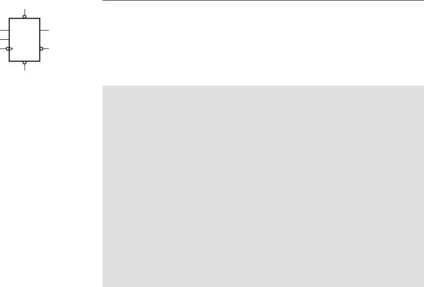
160 CHAPTER FOUR sequential basics
We have now covered the main aspects of flip-flops and registers.
There are other extensions, but they are just variations on the themes we
have seen. One such variation is the addition of a control input to preset
a flip-flop to 1. This is much like a reset control input, and may be either
synchronous or asynchronous. Another variation is for the reset control
input to use active-low logic, that is, for a 0 on the reset input to clear the
stored data and output. Likewise, a preset control input might use active-
low logic. A further variation is to use active-low logic for the clock input.
This involves triggering a change of stored value on a falling edge of the
clock signal rather than on a rising edge.
example 4.3 The symbol in Figure 4.10 shows a negative-edge-triggered
fl ip-fl op with clock enable, negative-logic asynchronous preset and clear, and
both active-high and active-low outputs. It is illegal for both preset and clear to
be active together. Develop a Verilog model for this fl ip-fl op.
solution The module definition is
module flip_flop_n ( output reg Q,
output Q_n,
input pre_n, clr_n, D,
input clk_n, CE );
always @( negedge clk_n or
negedge pre_n or negedge clr_n ) begin
if (!pre_n && !clr_n)
$display("Illegal inputs: pre_n and clr_n both 0");
if (!pre_n) Q <= 1'b1;
else if (!clr_n) Q <= 1'b0;
else if (CE) Q <= D;
end
assign Q_n = ~Q;
endmodule
We adopt the convention of appending “_n” to a name to indicate active-low
logic. The always block models the flip-flop behavior. Since the
pre_n and clr_n
inputs are asynchronous control inputs, we include them, along with the clock
input, in the event list of the block. Since they are all active-low inputs, we use
negedge to specify that the block should respond to negative (falling) edges, that
is, to changes from 1 to 0. Within the block, we check that the illegal condition
described in the specification does not arise during use of the flip-flop in a
circuit. The remainder of the block is based on the template for a flip-flop with
asynchronous control. In this case, we have two asynchronous control inputs, so
D
CE
Q
Q
pre
clr
clk
FIGURE 4.10 A negative-
edge-triggered fl ip-fl op.
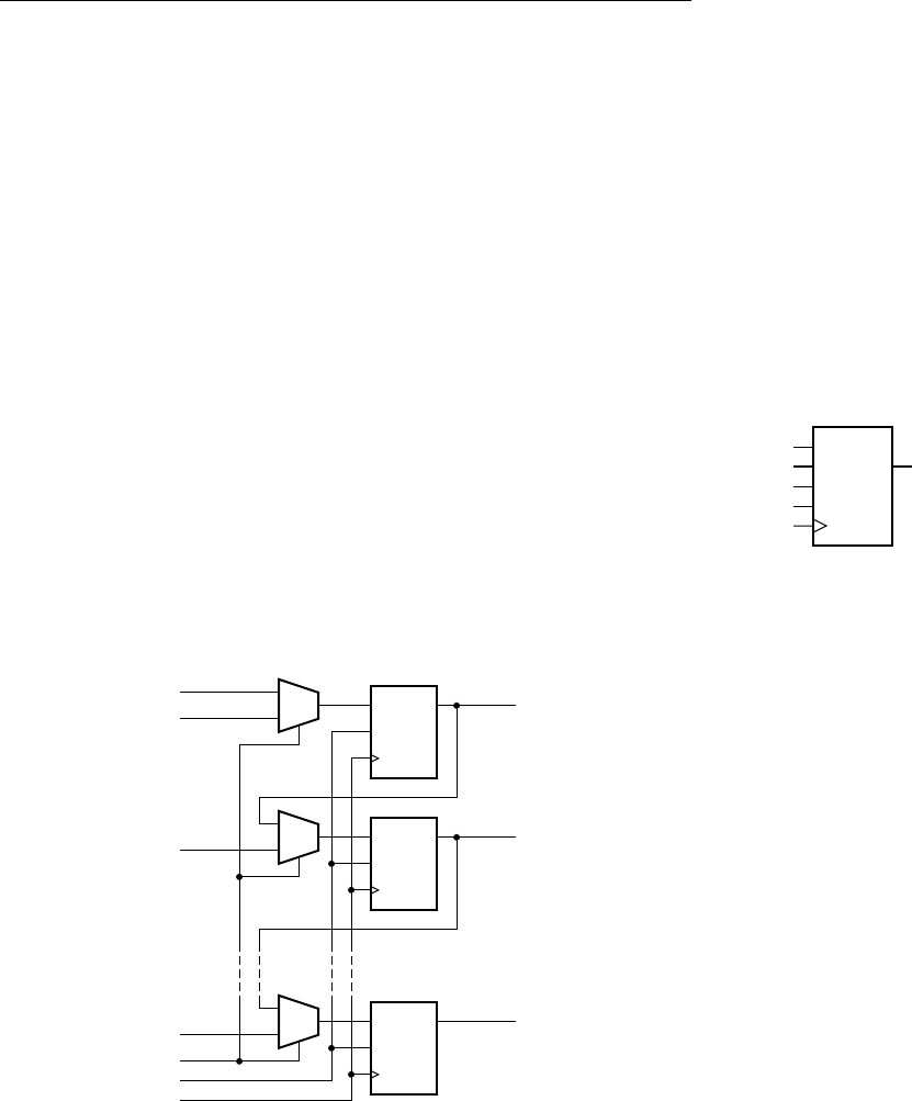
we test them, one after the other, before checking for the synchronous
clock-enable control input.
4.1.2 SHIFT REGISTERS
A register, as we have seen, stores data and makes it available at the out-
put unchanged. A shift register, on the other hand, can perform a shift
operation on the stored data. We described shift operations in Chapter 3,
and showed how a shift operation has the effect of scaling a numeric value
by a power of 2. As we will see in Chapter 8, shift operations are also used
to implement serial transfer of data, that is, transfer one bit at a time over
a single wire, instead of using separate wires for each of the bits of data.
For now, we will just focus on use of shift registers to combine arithmetic
scaling with storage functions.
Figure 4.11 shows a symbol for a shift register, and Figure 4.12 shows
how it can be implemented with D flip-flops and multiplexers. The shift
register is updated on a rising clock edge when
CE is 1. In that case, when
the load_en signal is 1, the multiplexers select new data on the D(n–1)
through
D(0) inputs for updating the register. Alternatively, when CE is 1
and load_en is 0, the multiplexers select the existing data, shifted right by
one place. The least significant bit is discarded, and the most significant
bit is updated with the value of the D_in signal. If we tie D_in to 0, the
shift register performs a logical shift right operation on the stored data.
Alternatively, if we connect the most significant output bit back to D_in,
the shift register performs an arithmetic shift right operation. We will see
in Chapter 8 how we connect the D_in input and the Q(0) output for serial
transfer of data.
4.1 Storage Elements CHAPTER FOUR 161
FIGURE 4.11 A symbol for a
shift register.
D
D_in
CE
load_en
Q
clk
FIGURE 4.12 A shift regis-
ter implemented with D fl ip-fl ops
and multiplexers.
D
CE
Q
0
1
D
CE
Q
0
1
D
CE
Q
0
1
Q(n–1)
Q(n–2)
Q(0)
D(n–1)
D(n–2)
D(0)
clk
CE
load_en
D_in
clk
clk
clk
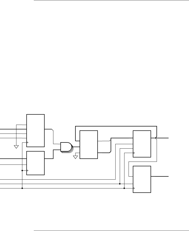
162 CHAPTER FOUR sequential basics
example 4.4 In Chapter 3, we showed how to perform multiplication of
unsigned integers by addition of partial products. Construct a multiplier for two
16-bit operands containing just one adder that adds successive partial products
over successive clock cycles. The fi nal product is 32 bits.
solution In order to perform the operation over multiple cycles, we need
a number of registers to hold intermediate results, as shown in Figure 4.13. The
x operand is stored in an ordinary register whose output connects to an array
of 16 AND gates that form a partial product. The
y operand is stored in a shift
register whose least significant bit,
Q(0), controls the AND gates. The y operand
is shifted on successive cycles, thus giving the 16 successive partial products. The
sum of the partial products are accumulated in a 17-bit ordinary register and a
15-bit shift register. Since the shift register is never required to load data other
than through the
D_in connection, the data and load_en inputs are absent. On
each clock cycle, the least significant bit of the ordinary register is shifted into
the shift register, and the remaining bits of the ordinary register are added with
the next partial product. By shifting the accumulated sum in this way, partial
products are added at successively more significant positions of the result.
FIGURE 4.13 Registers, shift
registers and other components
used to form a sequential
multiplier.
17-bit reg
reset
CE
DQ
D
16-bit reg
CE
Q
D_in
15-bit
shift reg
CE
Q
16-bit
shift reg
D_in
D
CE
load_en
Q
x
16-bit
adder
c0
y
c16
s
15...0
16
15
0
31...16
P(14...0)
P(31...15)
y(15...0)
x(15...0)
y_load_en
y_ce
x_ce
P_reset
P_ce
clk
clk
clk
clk
clk
Making the sequential multiplier perform the required operations over successive
clock cycles requires a separate control circuit. We will discuss control sequenc-
ing in detail in Section 4.3, and leave detailed design of the multiplier control to
Exercise 4.20.
4.1.3 LATCHES
As we have seen, a flip-flop is a basic sequential circuit element that stores
one bit. Most digital circuits use edge-triggered flip-flops that store a new
data value when the clock signal changes from 0 to 1. No further values
are stored while the clock remains at 1, nor when the clock returns to 0.
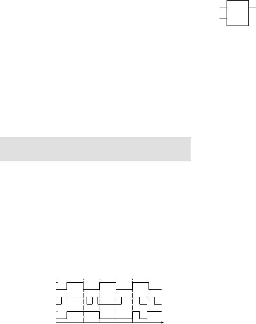
Some systems, however, use sequential elements called latches, with
slightly different timing for storage of values. Figure 4.14 shows a symbol
for a latch, and Figure 4.15 shows the timing behavior.
The latch has two inputs, a data input, D, and a latch-enable input,
LE. It also has a data output, Q. When the latch-enable input is 1, the
value at the data input is stored in the latch and transmitted through to
the output. As the timing diagram shows, provided the data input remains
unchanged for the entire time that the latch-enable input is 1, the behavior
is the same as that of a flip-flop. However, if the data input changes while
the latch-enable input is 1, the changed value is transmitted to the output.
When the latch-enable input eventually changes to 0, the value stored
in the latch just before the change is maintained in the latch and at the
output. The fact that data is transmitted through to the output while the
latch-enable input is 1 leads us also to use the name transparent latch
for this component. While the latch-enable input is 1, what we see on
the output is the value present on the input, so the latch appears to be
transparent.
We can model a latch in Verilog using an always block of the form
always @(LE or D)
if(LE) Q <= D;
This block includes both the latch-enable input and the data input in the
event list. The notation or in the event list specifies that the block responds
to changes on either input. However, it only updates the output Q when
LE is 1. If the D input changes while the LE input is 1, the change on D is
reflected on the output, modeling the transparent state of the latch. On
the other hand, if D changes while LE is 0, the output is not assigned and
maintains its previous value.
Just as we can implement multibit registers with flip-flops connected
in parallel, so we can implement multibit latches with single-bit latches
connected in parallel. The result is a latch in which multiple data bits flow
through when the latch-enable input is 1 and are stored when the latch-
enable input is 0.
4.1 Storage Elements CHAPTER FOUR 163
FIGURE 4.14 Symbol for a
latch.
DQ
LE
D
LE
Q
FIGURE 4.15 Timing
diagram for a latch.
While latch circuits are relatively simple to implement in many fabrics,
the fact that data can flow through them transparently can make it harder
to design complex systems with correct timing behavior. The usual solu-
tion is to use two-phase nonoverlapping clock signals. Since this approach
is not widely used now, the details are beyond the scope of this book. (See
the books in Section 4.6, Further Reading.) However, we do need to con-
sider how latching behavior can arise inadvertently from Verilog models,
since it is a common design error.
First, let’s return to our definition of a combinational logic circuit. We
said that such a circuit is one whose outputs are defined purely as a func-
tion of the current input values, and that have no dependence on previous
input values. The way in which a circuit’s output can depend on previous
input values is for the circuit to have a feedback path, that is, a cycle of
connections from the output of a gate through other gates and back to the
input of the gate. Perhaps the simplest such circuit is an inverter whose
output is connected to its input, as shown at the top of Figure 4.16. Since
the output of the inverter is the logical negation of its input, the output
will oscillate between 0 and 1 with a frequency that is dependent on the
propagation delay through the inverter. (Alternatively, the inverter may
exhibit analog circuit behavior and reach an intermediate voltage level
that is neither a valid logic low nor a valid logic high.) If we extend the
feedback loop with more inverters to give an odd number of inverters
in total (as shown at the bottom of Figure 4.16), we reduce the overall
frequency of oscillation. This form of oscillator is called a ring oscillator.
If we extend the ring to have an even number of inverters, the circuit will
reach a stable state in which alternate inverters have a 0 at their output
and the others have a 1. There are two possible stable states for such a
ring of inverters. We could force the ring into one or other of the states by
forcing a given node to 0 or 1, for example, by using switches as shown in
Figure 4.17. (This is an idealization. In a real circuit, the switches would
have some series resistance, thus avoiding damage to the output of the
second inverter.) When both switches are open, the circuit retains the state
into which is was forced. Hence, its output depends on the previous input
value. This is a basic form of one-bit storage, called a reset-set latch, or
RS-latch for short.
A more common implementation of an RS-latch uses cross-coupled
gates, as shown in Figure 4.18. The timing behavior of the RS-latch is
shown in Figure 4.19. Normally, the reset input R and the set input S
are both 0. Assume initially that Q is 0 and
_
Q is 1. This is a stable state,
called the reset state. If the
R input changes to 1 in this state, neither out-
put changes and the latch stays in the reset state. However, if the S input
changes to 1,
_
Q changes to 0. This value is fed back to the other gate,
which causes Q to change to 1. This is also a stable state, called the set
state. When S returns to 0, the latch stays in the set state. Further changes
FIGURE 4.16 Inverters
connected in feedback loops.
FIGURE 4.17 Using switches
to force a node of an inverter ring
to 0 or 1.
+V
FIGURE 4.18 Cross-coupled
RS-latch.
Q
Q
R
S
164 CHAPTER FOUR sequential basics
4.1 Storage Elements CHAPTER FOUR 165
Q
S
R
Q
reset reset setset illegal
FIGURE 4.19 Timing for an
RS-latch, showing the reset and
set states, as well as an illegal
operating condition.
of S to 1 while the latch is in the set state make no difference. However, if
R goes to 1, the feedback causes the latch to change back to the reset state.
Thus, which state the latch is in at any time depends on which of the S or
R inputs was 1 most recently. Note that if both R and S are 1 at the same
time, both Q and
_
Q are 0. This is usually considered an illegal operating
condition for an RS-latch.
Now that we have seen ways in which feedback can cause latching
behavior, let’s see how feedback can arise in Verilog models. In Chapter 2,
we showed how a combinational circuit is modeled using an assignment
statement in an architecture. Normally, we include the inputs to the
circuit in the expression on the right-hand side of the assignment symbol
and the output of the circuit on the left-hand side. However, if we have
an assignment with a given net appearing both on the left-hand side
and on the right-hand side, we imply a feedback loop from the output
to the input. Most synthesis CAD tools will not synthesize such circuits
without complaint, since the timing is not readily predictable and correct
operation is not guaranteed. For example, if we write the following in a
model:
assign a = a + b;
we imply an adder with the output feeding back directly into an input.
In this sense, assignments modeling combination hardware in Verilog
are different from assignments to variables in programming languages.
Depending on the propagation delay through the synthesized and imple-
mented circuit, we may add the value of b to itself once, twice, or more
times within a given time interval. Moreover, if the delays are different
for different bits, the result may not correspond to addition of the value
of
b at all. Most synthesis tools would either issue a warning or reject an
assignment in the above form as erroneous.

166 CHAPTER FOUR sequential basics
A feedback loop can also be implied by a number of assignments in
combination, where there is a cycle of dependencies between them. For
example, consider the following assignments:
assign x = y + 1;
assign y = x + z;
Due to the first assignment, the value of x depends on the value of y. Due
to the second assignment, the value of x depends on y, and thus indirectly
on x itself. A synthesis tool should also issue a warning or flag this as
erroneous.
The fact that synthesis tools object to feedback loops in combina-
tional circuits can make it hard to model circuits in which we deliberately
include such loops. For example, a Verilog model of the cross-coupled
RS-latch of Figure 4.18 might be written as
assign Q = ~(R | Q_n);
assign Q_n = ~(S | Q);
These assignments imply a cyclic dependency between Q and Q_n, which is
exactly what we want in the synthesized circuit. An alternative way of mod-
eling this behavior is to use an always block and an assignment, as follows:
always @(R or S)
if (R) Q <= 1'b0;
else if (S) Q <= 1'b1;
assign Q_n = Q;
The assignment simply negates the value of Q, which is generated by the
always block. In the block, we have included the R and S inputs in the event
list. Thus, the block will be reactivated whenever either input changes. If R
is 1, the block updates the Q output to represent the reset state, and if S is 1,
the block updates the output to represent the set state. Note that, if neither
input is 1, the block makes no assignment to Q. In that case, the outputs
remain unchanged; that is, it stores the previously updated state. In gen-
eral, if there is any execution path through an always block where we do
not update an output, then the block represents latching behavior for that
output, since the output maintains its previous value. If this is intended, as
in the block modeling the RS-latch, we don’t have a problem. However, it
is a common Verilog modeling error to inadvertently omit an assignment

to an output in an execution path, for example, in one alternative of a
complex if statement. The unintended latching behavior for that output
can be most perplexing until the error is located and corrected.
example 4.5 The following always block is intended to model multi-
plexer circuitry that selects between a number of inputs to assign to outputs
z1
and z2. Identify the error in the block and describe the behavior that results.
always @*
if (~sel) begin
z1 <= a1; z2 <= b1;
end else begin
z1 <= a2; z3 <= b2;
end
solution The assignment to z3 in the “else” part of the if statement
should assign to
z2. As a consequence, z2 is not updated on that execution path
and
z3 is not updated on the execution path in which sel is 0. Thus, the block
implies transparent latches for
z2 and z3. The latch for z2 is transparent when
sel is 0 and stores a value when sel is 1. The latch for z3 is transparent when sel
is 1 and stores a value when sel is 0. This unintended behavior can be corrected
simply by changing the target of the assignment from
z3 to z2, as it should be.
1. Write a Verilog always block for a simple rising-edge-triggered register.
2. What do we call an arrangement of combinational subcircuits and
registers that operate in assembly-line-like fashion?
3. What effect does a clock-enable input have on a register?
4. What is the distinction between an asynchronous reset and a
synchronous reset?
5. What additional function does a shift register provide compared to
an ordinary register?
6. What is meant by the term “transparent” with respect to a latch?
7. What problem is caused by omitting an assignment to an output in
a Verilog always block that models combinational logic?
4.2 COUNTERS
A counter is a sequential component that increments or decrements a
stored value. Counters occur in many digital circuit applications. For
example, if an application requires a given operation to be performed on
KNOWLEDGE
TEST QUIZ
KNOWLEDGE
TEST QUIZ
4.2 Counters CHAPTER FOUR 167
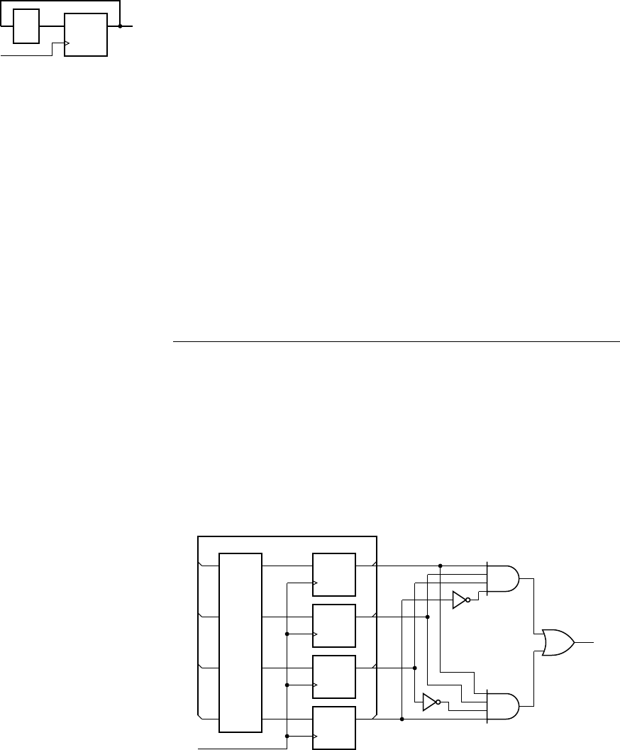
168 CHAPTER FOUR sequential basics
a number of items of data or to be repeated a number of times, a counter
can be used to keep track of how many items have been processed or how
many times the operation has been performed. Counters are also used as
timers, by counting the number of intervals of a fixed duration that have
passed.
A simple form of counter is composed of an edge-triggered register
and an incrementer, as shown in Figure 4.20. The value stored in the reg-
ister is interpreted as an unsigned binary integer. The incrementer can be
implemented using the circuit we described for an unsigned incrementer
in Section 3.1.2 on page 108. The counter increments the stored value on
every clock edge. When the stored count value reaches its maximum value
(2
n
1, for an n-bit counter), the incrementer yields a result of all zeros,
with the carry out being ignored. This result value is stored on the next
clock edge. Thus, the counter acts like the odometer in a car, rolling over
to zeros after reaching its maximum value. Mathematically speaking, the
counter increments modulo 2
n
. The counter goes through all 2
n
unsigned
binary integer values in order every 2
n
clock cycles. One use for such
a counter is in conjunction with a decoder to produce periodic control
signals.
example 4.6 Design a circuit that counts 16 clock cycles and produces a
control signal,
ctrl, that is 1 during every eighth and twelfth cycle.
solution We need a 4-bit counter, since 16 2
4
. The counter counts
from 0 to 15 and then wraps back to 0. During the eighth cycle, the counter
value is 7 (0111
2
), and during the twelfth cycle, the counter value is 11 (1011
2
).
We can generate the control signal by decoding the two required counter values
and forming the logical OR of the decoded signals. The required circuit is shown
in Figure 4.21.
DQ+1 Q
clk
clk
FIGURE 4.20 A simple
counter composed of a register
and an incrementer.
+1
clk
ctrl
0
1
2
3
0
1
2
3
DQ
DQ
DQ
DQ
clk
clk
clk
clk
FIGURE 4.21 A counter with
decoded outputs.
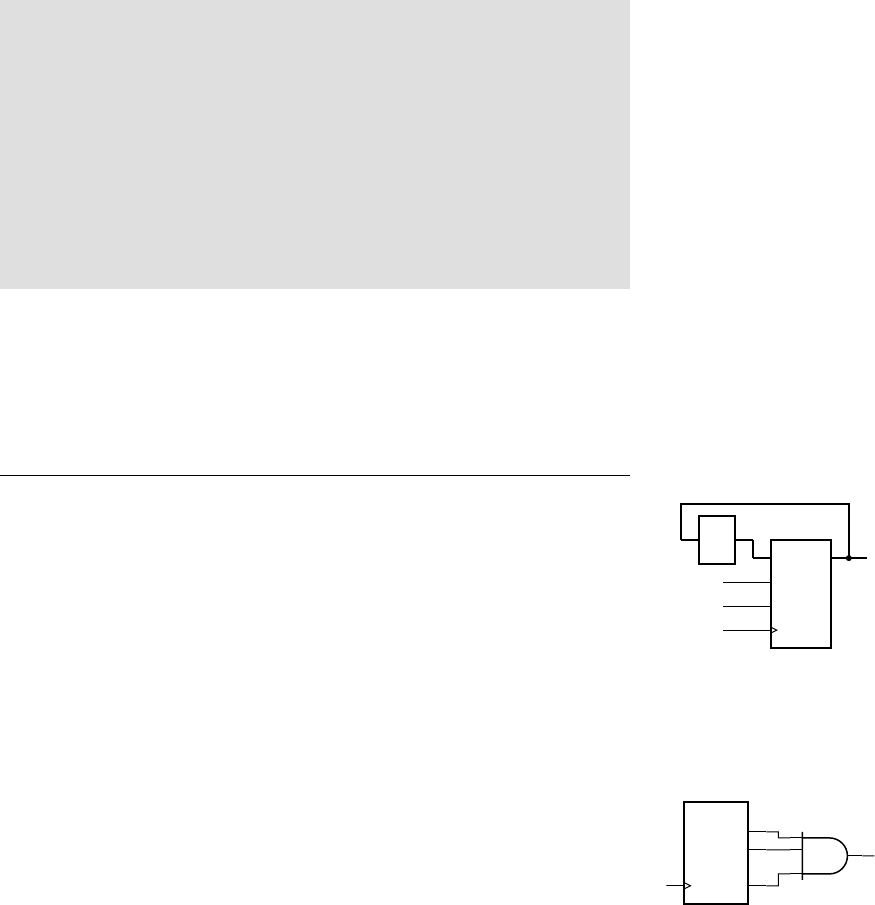
example 4.7 Develop a Verilog model of the circuit from Example 4.6.
solution The module definition is
module decoded_counter ( output ctrl,
input clk );
reg [3:0] count_value;
always @(posedge clk)
count_value <= count_value + 1;
assign ctrl = count_value = = 4'b0111 ||
count_value = = 4'b1011;
endmodule
The module contains an always block that represents the counter. It is similar
in form to a block for an edge-triggered register. The difference is that the value
assigned to the
count_value output on a rising clock edge is the incremented
count value. The assignment to
count_value represents the update of the value
stored in the register, and the addition of 1 represents the incrementer. The final
assignment statement in the module represents the decoder.
The counter that we have described so far is free running, increment-
ing the count value on every clock cycle. We can modify the counter to
make it useful in applications that require more control over the count
value. Two simple modifications involve adding a clock enable and a
reset input to the storage register within a counter. The clock-enable input
allows us to control when the counter increments its value, so this input
is often called a count-enable input. The reset input allows us to clear
the count value back to zero. A counter modified in this way is shown in
Figure 4.22. This form of counter is very useful for counting occurrences
of events. We would connect a signal indicating event occurrence to the
count-enable input of the counter. If we need to count events over several
intervals, we can reset the counter at the start of each interval.
Another modification is a terminal-count output. This is simply a
decoded output that is 1 when the counter reaches is maximum, or ter-
minal, value. For the counters we have described above, the maximum
value of 2
n
1 is represented by a count value with all 1 bits. We can use
an n-input AND gate to generate the terminal count output, as shown in
Figure 4.23. For a free-running counter, the terminal-count output is 1
for a single clock cycle every 2
n
clock cycles; that is, it is a periodic signal
whose frequency is the input clock frequency divided by 2
n
.
4.2 Counters CHAPTER FOUR 169
+1
Q
clk
CE
reset
D
CE
Q
reset
clk
FIGURE 4.22 A counter with
clock-enable and reset inputs.
counter
…
…
Q0
Q1
Qn
…
T
C
clk
FIGURE 4.23 A counter with
terminal-count output.
170 CHAPTER FOUR sequential basics
example 4.8 A digital alarm clock needs to generate a periodic signal at
a frequency of approximately 500Hz to drive the speaker for the alarm tone.
Use a counter to divide the system’s master clock signal, with a frequency of
1 MHz, to derive the alarm tone.
solution We need to divide the master clock signal by approximately
2000. We can use a divisor of 2
11
2048, which gives us an alarm tone fre-
quency of 488Hz, which is close enough to 500 Hz. Thus, we could use the
terminal-count output of an 11-bit counter for the tone signal. However, the
duty cycle (the ratio of time for which the signal is 1 to the time for which it
is 0) would only be 1/2048, which would have very low AC energy. We can
rectify this by dividing the master clock by 2
10
with a 10-bit counter, and using
the terminal-count output as the count-enable input to a divide-by-2 counter.
A circuit is shown in Figure 4.24, and a timing diagram in Figure 4.25. The
output of the divide-by-2 counter alternates between 0 and 1 for every pulse on
its clock-enable input. The output thus has a 50% duty cycle, which will drive a
speaker much more efficiently.
Not all free-running counter applications need to divide by a power
of 2. If we need to divide by some other value, k, we need the counter
to wrap back to 0 after reaching a terminal count of k 1. Mathemati-
cally speaking, the counter increments modulo k. We can construct such a
counter by decoding the unsigned binary code word for k 1 and using
that as the terminal count output. We can feed the terminal count sig-
nal back to a synchronous reset input to the storage register within the
counter.
count
tone2
tone
clk
10-bit
counter
Q
TC
D
CE
Q
clk
clk
FIGURE 4.24 An alarm clock
frequency divider.
tone
tone2
count
clk
11002 2 102 10
1023 1023 1023
FIGURE 4.25 Timing
diagram for an alarm clock
frequency divider.
example 4.9 Design a circuit for a modulo 10 counter, otherwise known
as a decade counter.
solution The maximum count value is 9, so we need 4 bits for the counter.
The unsigned binary code word for 9 is 1001
2
. We can decode this value and
use it to reset to counter to 0 on the next clock cycle. The circuit is shown in
Figure 4.26.
4.2 Counters CHAPTER FOUR 171
clk Q0
Q1
Q2
Q3
Q0
Q1
Q2
Q3reset
counter
clk
FIGURE 4.26 A decade
counter.
example 4.10 Develop a Verilog model for the decade counter of
Example 4.9.
solution The module definition is
module decade_counter ( output reg [3:0] q,
input clk );
always @(posedge clk)
q <= q = = 9 ? 0 : q + 1;
endmodule
We model the output port for the count value using an unsigned vector, since
it is represents a binary-coded integer value. On a rising clock edge, the always
block checks whether the counter has reached the terminal count value. If so,
the count value wraps back to 0; otherwise, the block adds 1 to yield the new
count value.
Another form of counter that is useful in timing applications is a
down counter with load. This counter is loaded with an input value, and
then decrements the count value. The terminal count output is activated
when the count value reaches zero. A circuit for the counter is shown in
Figure 4.27. It consists of a register whose input comes either from the
input value to be loaded or from the decremented count value. In this
case, the loading of input data is synchronous, since it occurs on a rising
clock edge.
172 CHAPTER FOUR sequential basics
If the clock input to the counter is a periodic signal with period t and
the counter is loaded with a value k, the terminal count is reached after
an interval of k t. Thus, this form of counter can be used as an interval
timer, where the terminal-count output signal is used to trigger an activity
after expiration of a given time interval.
example 4.11
Develop a Verilog model for an interval timer that has
clock, load and data input ports and a terminal-count output port. The timer
must be able to count intervals of up to 1000 clock cycles.
solution The data input and counter need to be 10 bits wide, since that is
the minimum number of bits needed to represent 1000. The module definition is
module interval_timer_rtl ( output tc,
input [9:0] data,
input load, clk );
reg [9:0] count_value;
always @(posedge clk)
if (load) count_value <= data;
else count_value <= count_value – 1;
assign tc = count_value = = 0;
endmodule
On a rising clock edge, the always block uses the load input to determine
whether to update the count value with the data input or the decremented
count value. The decrement operation is performed using an unsigned subtrac-
tion without borrow out. So after reaching zero, the count value wraps back to
the largest 10-bit value, namely, 1023. The final assignment in the architecture
drives the terminal count to 1 when the count value reaches zero.
example 4.12 Modify the interval timer so that, when it reaches zero, it
reloads the previously loaded value rather than wrapping around to the largest
count value.
DQ
–1
=0?
Q
TC
clk
load
D
0
1
clk
FIGURE 4.27 A down
counter with synchronous load.
solution We need to use a separate register to store the data value to load
into the counter. When the load input is activated, a new data value is loaded
into the storage register as well as into the counter. When the terminal count is
reached, the counter should be loaded from the storage register. The inputs and
outputs of the revised interval timer are the same, so we don’t need to change the
ports of the module definition. The revised module is
module interval_timer_repetitive ( output tc,
input [9:0] data,
input load, clk );
reg [9:0] load_value, count_value;
always @(posedge clk)
if (load) begin
load_value <= data;
count_value <= data;
end
else if (count_value = = 0)
count_value <= load_value;
else
count_value <= count_value – 1;
assign tc = count_value = = 0;
endmodule
In this module, we have added a separate variable, load_value, to represent the
storage register. The always block is revised so that, when
load is 1 on a ris-
ing clock edge, both the
load_value variable and the count_value variable are
updated from the
data input. Also, when the count value is 0 on a rising clock
edge (provided
load is not 1), the count value is updated from the load_value
variable. Otherwise, the count value is decremented as before.
The last kind of counter that we will describe in this section is a ripple
counter (distinct from ripple carry used in an incrementer of a counter),
shown in Figure 4.28. It is somewhat different in structure from the syn-
chronous counters we have previously examined. Like those counters, it
has a collection of flip-flops for storing the count value. However, unlike
them, the clock signal is not connected in common to all of the flip-flop
clock inputs. Rather, the clock input just triggers the flip-flop for the
least significant bit, causing it to toggle between 0 and 1 on each rising
clock edge. When the Q output changes to 0, the
_
Q output changes to
1, triggering the next flip-flop to toggle between 0 and 1. This flip-flop
behaves similarly, causing the third flip-flop to toggle when it (the second
4.2 Counters CHAPTER FOUR 173
D
Q
Q
D
Q
Q
D
Q
Q
D
Q
Q
Q0
Q1
Q2
Qn
clk
clk
clk
clk
clk
FIGURE 4.28 Structure of a
ripple counter.
174 CHAPTER FOUR sequential basics
flip-flop) changes from 1 to 0. In general, we can think of the flip-flops for
bits 0 to i 1 as forming an i-bit counter. The most significant bit of this
counter changes from 1 to 0 when it overflows. When that happens, the
next flip-flop, for bit i, toggles between 0 and 1. This behavior is shown
in the timing diagram of Figure 4.29.
An important timing issue arises from the fact that the flip-flops in a
ripple counter are not all clocked together. Each flip-flop has a propagation
delay between a rising edge occurring on its clock input and the outputs
changing value. These propagation delays are shown in Figure 4.29.
Since each flip-flop is clocked from the output of the previous flip-flop,
the propagation delays accumulate. The outputs of the counter don’t all
change at once on a change of the counter’s clock input. Instead, the out-
put changes “ripple” along the counter as they propagate through the
flip-flops; hence, the name of this kind of counter. The shaded areas in the
timing diagram show intervals where the count value is not correct, due to
changes not having propagated completely through the counter. Whether
this lack of synchronization among output changes is a problem or not
depends on the particular application under consideration. Some factors
to consider include:
The length of the counter. For longer counters, there are more flip-
flops through which changes have to propagate, making the maxi-
mum accumulated delay larger. For short counters, the delay may
be acceptable.
The period of the input clock relative to the propagation delays of
the counter. For a short clock period, the accumulated delay may
exceed the clock period. In that case, there will be clock cycles dur-
ing which the counter outputs don’t reach the correct value before
the end of the cycle. For systems with long clock periods, the count
value will settle early in the clock cycle.
왘
왘
Q1
Q0
Q0
clk
Q1
Q2
Q2
FIGURE 4.29 Timing
diagram for a ripple counter.
The tolerance for transient incorrect count values. If the count value
may be sampled before it has settled, incorrect operation may result.
However, if the count value is not sampled until it is guaranteed
settled, operation is correct.
The main advantages of a ripple counter are that it uses much less
circuitry in its implementation (since an incrementer is not required) and
that it consumes less power. Hence, it is useful in those applications that
are sensitive to area, cost and power and that have less stringent timing
constraints. As an example, a digital alarm clock might use ripple coun-
ters to count the time, since changes occur infrequently relative to the
propagation delay (seconds compared to nanoseconds).
1. Show in a diagram how an incrementer and a register can be
connected to form a simple counter.
2. What is the maximum count value for an n-bit counter? What value
does it then advance to?
3. How is a modulo k counter constructed?
4. What is a decade counter?
5. What is an interval timer?
6. Why might a long ripple counter be unsuitable for an application
with a fast clock?
4.3 SEQUENTIAL DATAPATHS
AND CONTROL
We have now arrived at a key point in our discussion of digital logic
design. We have seen how information can be binary encoded, how
encoded information can be operated upon using combinational circuits,
and how encoded information can be stored using registers. We have also
seen that registers are needed both to avoid feedback loops in combina-
tional circuits and to deal with data that arrives at the inputs sequentially.
We have discussed counters as examples of combining registers and com-
binational circuits to perform sequential operations, that is, operations
that proceed over a number of discrete intervals of time. We are now
in a position to take a more general view of sequential operations. This
general view will form the basis of our subsequent discussions of digital
systems and embedded systems.
In many digital systems, the operations to be performed on input data
are expressed as a combination of simpler operations, such as arithmetic
operations and selection between alternative data values. Our general view
of a digital system divides the circuit that implements the operations into a
왘
KNOWLEDGE
TEST QUIZ
KNOWLEDGE
TEST QUIZ
4.3 Sequential Datapaths and Control CHAPTER FOUR 175

176 CHAPTER FOUR sequential basics
datapath and a control section. The datapath contains the combinational
circuits that implement the basic operations and the registers that store
intermediate results. The control section generates control signals that
govern the operation of the datapath elements: selecting operations to
be performed and enabling registers. In particular, the control section
ensures that control signals are activated in the right order and at the right
times to cause the datapath to perform the required operations on the
data flowing through it. Hence, we say that the control section performs
control sequencing. In many cases, the control section makes use of status
signals generated by the datapath. The status signals indicate whether cer-
tain conditions of interest are true, for example, whether data has certain
values, or whether input data is available. The values of the status signals
can influence the control sequence.
One of the most challenging tasks in digital design is designing a data-
path and corresponding control section to meet the given requirements
and constraints. There are usually many alternative datapaths that could
meet the functional requirements. Choosing among them usually involves
trading off between area and performance.
example 4.13 Develop a datapath to perform a complex multiplication
of two complex numbers. The operands and product are all in Cartesian form.
The real and imaginary parts of the operands are represented as signed fi xed-
point numbers with 4 pre-binary-point and 12 post-binary-point bits. The real
and imaginary parts of the product are similarly represented, but with 8 pre-
binary-point and 24 post-binary-point bits. The complex multiplier is subject to
constraints that strongly limit the circuit area.
solution Given two complex numbers a a
r
ja
i
and b b
r
jb
i
, the
complex product is
p abp
r
jp
i
( a
r
b
r
a
i
b
i
) j(a
r
b
i
a
i
b
r
) (4.1)
This computation requires four fixed-point multiplications, one subtraction and
one addition. If we were to implement the complex multiplier as a combinational
circuit, separate components would be needed for each of these operations,
consuming a large amount of circuit area. Since area is a strong constraint, we
can reduce the area by using one multiplier to perform the four multiplications
in sequence, and one adder/subtracter to form the real and imaginary parts of
the product. We will need registers to store the intermediate results. The full
computation will take place over several clock cycles.
A datapath to perform the sequential complex multiplication is shown in
Figure 4.30. Since the multiplier is shared, multiplexers at the multiplier inputs
are needed to select the operands. The result of a given multiplication is stored
in one or other of the partial-product registers. To form the real part of the
complex product, two partial products are subtracted by the adder/subtracter.
In the diagram, the signals upon which data flows are drawn with thicker lines,
since they carry multibit binary-coded values. The remaining signals, drawn with
lighter weight lines, are the clock and the control signals. They include select
signals for the multiplexers, clock-enable signals for the registers, and a signal
to choose the operation to be performed by the adder/subtracter. The values of
the control signals are driven by a separate control section, not shown on the
diagram.
example 4.14 Develop a Verilog model of the complex multiplier
datapath.
solution The module includes ports for the data inputs and outputs, as
well as clock and reset inputs and an input to indicate the arrival of new data.
We will return to the last of these inputs later. The module definition is
4.3 Sequential Datapaths and Control CHAPTER FOUR 177
0
1
0
1
D
CE
Q
D
CE
Q
×±
D
CE
Q
D
CE
Q
p_r
p_i
a_r
a_i
b_r
b_i
a_sel
b_sel
pp1_ce
pp2_ce
sub
p_r_ce
p_i_ce
clk
clk
clk
clk
clk
FIGURE 4.30 Datapath for a
sequential complex multiplier.
module multiplier
( output reg signed [7:-24] p_r, p_i,
input signed [3:-12] a_r, a_i, b_r, b_i,
input clk, reset, input_rdy );
reg a_sel, b_sel, pp1_ce, pp2_ce, sub, p_r_ce, p_i_ce;
wire signed [3:-12] a_operand, b_operand;
wire signed [7:-24] pp, sum;
reg signed [7:-24] pp1, pp2;
...
(continued)
To form the imaginary part, two partial products are added. In each case, the
part of the complex product is stored in an output register.

178 CHAPTER FOUR sequential basics
The nets and variables declared within the module represent the control signals
and the internal data connections. There are further declarations for the control
section that we will return to later. In the statement part of the architecture, the
assignments to
a_operand and b_operand represent the multiplexers, and the
assignment to
pp represents the multiplier. (The multiplier operands are extended
so that the result size matches the sizes of the real and imaginary parts of the
product.) The first two always blocks represent the partial-product registers. The
assignment to
sum represents the adder/subtracter, and the second two always
blocks represent the output registers. We will return to further statements that
represent the control section later.
example 4.15 Design a control sequence for the control signals of the
sequential complex multiplier.
solution We first need to determine a sequence of operations to be
performed by the datapath to implement the required function expressed in
Equation 4.1. There are many possible sequences, but we must ensure that there
is no conflict for resources; that is, we must ensure that we don’t try to use an
element of the datapath for more than one operation at a time. One possible
sequence, initiated by
input_rdy being 1, is:
1. Multiply a_r and b_r, and store the result in partial product register 1.
2. Multiply a_i and b_i, and store the result in partial product register 2.
assign a_operand = ~a_sel ? a_r : a_i;
assign b_operand = ~b_sel ? b_r : b_i;
assign pp = {{4{a_operand[3]}}, a_operand, 12'b0} *
{{4{b_operand[3]}}, b_operand, 12'b0};
always @(posedge clk) // Partial product 1 register
if (pp1_ce) pp1 <= pp;
always @(posedge clk) // Partial product 2 register
if (pp2_ce) pp2 <= pp;
assign sum ~sub ? pp1 + pp2 : pp1 – pp2;
always @(posedge clk) // Product real-part register
if (p_r_ce) p_r <= sum;
always @(posedge clk) // Product imaginary-part register
if (p_i_ce) p_i <= sum;
...
endmodule

3. Subtract the partial product register values and store the result in the
product real part register.
4. Multiply
a_r and b_i, and store the result in partial product register 1.
5. Multiply a_i and b_r, and store the result in partial product register 2.
6. Add the partial product register values and store the result in the product
imaginary part register.
This sequence would take six clock cycles to complete. In each cycle, only one of
the arithmetic components is used, so there is no conflict for resources. However,
we can reduce the number of cycles required, without creating conflict, by using
the multiplier and the adder/subtracter concurrently. Specifically, we can merge
steps 3 and 4 into one step, in which we subtract partial products to form the
real part of the product and we multiply
a_r and b_i to form a further partial
product.
Given this 5-step sequence, the control signals that need to be activated in
each step are shown in Table 4.1. The combination of control signal values in
each step cause the datapath components to perform the required operations
for that step. Note that in some steps, the multiplexers and adder/subtracter are
not used. We don’t care what values are driven for the control signals governing
those components in those steps.
4.3 Sequential Datapaths and Control CHAPTER FOUR 179
4.3.1 FINITE-STATE MACHINES
Example 4.15 describes a control sequence for a sequential datapath, but
we have yet to show how to design a circuit for the control section that
generates the control sequence. We will introduce an abstraction called
a finite-state machine for this purpose. There is a substantial body of
mathematical theory underlying finite-state machines. Some of the useful
results from this theory are implemented in CAD tools that transform
finite-state machines to optimize sequential circuits. However, we will
take a pragmatic approach, focusing on the design of control sections to
sequence the operation of datapaths.
step a_sel b_sel pp1_ce pp2_ce sub p_r_ce p_i_ce
10010–00
21101–00
30110110
41001–00
5– –00001
TABLE 4.1 Control sequence
for the complex multiplier.

180 CHAPTER FOUR sequential basics
D
reset
Q
current_state
outputs
inputs
clk
reset
next
state
logic
output
logic
clk
FIGURE 4.31 Circuit structure
for a fi nite-state machine.
In general terms, a finite-state machine is defined by a set of inputs,
a set of outputs, a set of states, a transition function that governs transi-
tions between states, and an output function. The states are just abstract
values that mark steps in a sequence of operations. The machine is called
“finite-state” because the set of states is finite in size. The finite-state
machine has a current state in a given clock cycle. The transition function
determines the next state for the next clock cycle based on the current
state and, possibly, the values of inputs in the given clock cycle. The out-
put function determines the values of the outputs in a given clock cycle
based on the current state and, possibly, the values of inputs in the given
clock cycle.
Figure 4.31 shows a schematic representation of a finite-state machine.
The register stores the current state in binary coded form. One of the states
in the state set is designated the initial state. When the system is reset, the
register is reset to the binary code for the initial state; thus, the finite-state
machine assumes the initial state as its current state. During each clock
cycle, the value of the next state is computed by the next state logic, which
is a combinational circuit that implements the transition function. Also,
the outputs are driven with the value computed by the output logic, which
is a combinational circuit that implements the output function. The out-
puts are the control signals that govern operation of a datapath. On the
rising clock edge marking the beginning of the next clock cycle, the cur-
rent state is updated with the computed next-state value. The next state
may be the same as the previous state, or it may be a different state.
Finite-state machines are often divided into two classes. In a Mealy
finite-state machine, the output function depends on both the current
state and the values of the inputs. In such a machine, the connection
drawn with a dashed line in Figure 4.31 is present. If the input values
change during a clock cycle, the output values may change as a conse-
quence. In a Moore finite-state machine, on the other hand, the output
function depends only on the current state, and not on the input values.
The dashed connection in Figure 4.31 is absent in a Moore machine. If the
input values change during a clock cycle, the outputs remain unchanged.

In theory, for any Mealy machine, there is an equivalent Moore machine,
and vice versa. However, in practice, one or the other kind of machine will
be most appropriate. A Mealy machine may be able to implement a given
control sequence with fewer states, but it may be harder to meet timing
constraints, due to delays in arrival of inputs used to compute the next
state. As we present examples of finite-state machines, we will identify
whether they are Mealy or Moore machines.
In many finite-state machines, there is an idle state that indicates
that the system is waiting to start a sequence of operations. When an
input indicates that the sequence should start, the finite-state machine
follows a sequence of states on successive clock cycles, with the output
values controlling the operations in a datapath. Eventually, when the
sequence of operations is complete, the finite-state machine returns to
the idle state.
example 4.16 Design a fi nite-state machine to implement the control
sequence for the complex multiplier described in Example 4.15. The control
sequence is initiated by
input_rdy being 1 during the clock cycle in which new
data arrives at the datapath inputs.
solution Our finite-state machine needs five states, one for each of the
steps of the control sequence. Let’s call them
step1 through step5. We also need
to deal with the case of waiting for input data to arrive. We could consider a
separate idle state for that case. When, in the idle state,
input_rdy is 1, we would
then transition to
state1 to start the multiplication; otherwise, we would stay
in the idle state. The problem with this is that it wastes a clock cycle, since we
would not perform the first multiplication until after the cycle in which data
arrived.
The alternative is to use
step1 as the idle state. If it turns out that new data has
not arrived in a given clock cycle while in this state, we simply repeat
step1 as
the next state. On the other hand, if new data has arrived, indicated by
input_rdy
being 1 in the clock cycle, the real parts are multiplied during that clock cycle
and can be stored on the next clock edge. We would then transition to
step2,
and on subsequent clock cycles to
step3, step4 and step5. At the end of the
step5 clock cycle, the complete complex product is stored in the output registers
of the datapath, so we can transition back to
step1 in the next clock cycle.
In summary, our finite-state machine has the signal input_rdy as its single input,
and the control signals listed in Example 4.15 as outputs. The state set is {
step1,
step2, step3, step4, step5}, with step1 being the initial state. The transition
function is defined in Table 4.2. The output function is defined in Table 4.1.
Since the output function depends only on the current state and not on the input
value, this finite-state machine is a Moore machine.
4.3 Sequential Datapaths and Control CHAPTER FOUR 181
current_
state
input_
rdy
next_
state
step1 0 step1
step1 1 step2
step2 – step3
step3 – step4
step4 – step5
step5 – step1
TABLE 4.2 The transition
function for the complex multiplier
fi nite-state machine.

182 CHAPTER FOUR sequential basics
An important issue to consider when designing a finite-state machine
is how to encode the state values. We glossed over that in Example 4.16
by treating the states as abstract values. As we discussed in Chapter 2,
if we have N states, we need at least ⎡log
2
N⎤ bits in our code. However,
we may choose to have more if that simplifies circuitry that uses encoded
states. In particular, while a longer than minimal code length requires
more flip-flops in the state register and more wires for the state signals,
it may make the next-state and output logic circuits simpler and smaller.
In general choosing an optimal state encoding is a complex mathematical
problem. However, synthesis CAD tools incorporate methods for choos-
ing a state encoding, so we may be able to let a tool make the choice for
us. One aspect of state encoding is the choice of a code word to represent
the initial state. In many cases, a good choice is a code word with all 0
bits, since that allows us to use a simple register with reset for the state
register. If some other code word is chosen for the initial state, that code
word must be loaded into the register on system reset.
Modeling Finite-State Machines in Verilog
Since a finite-state machine is composed of a register, next-state logic and
output logic, a straightforward way to model a finite-state machine is
to use the Verilog features that we already know for modeling registers
and combinational logic. The only aspect we have not addressed is how
to represent the state set, particularly when we want to take an abstract
view and leave state encoding to the synthesis tool. In Verilog, we can use
parameter definitions to specify a set of symbolic names associated with
the binary code words for the states. For example, we can define param-
eters for the states in Example 4.16 as follows:
parameter [2:0] step1 = 3'b000, step2 = 3'b001,
step3 = 3'b010, step4 = 3'b011,
step5 = 3'b100;
This defines five parameters, named step1 through step5, corresponding
to the binary code words 000 through 100, respectively. In the rest of the
state machine model, we just use the symbolic names, not the code word
values. A synthesis tool may be able to recode the state parameters, that is,
to choose an alternate encoding for the state set, to optimize the generated
hardware for the state machine.
We can declare a variable to represent the current state of a state
machine as follows:
reg [2:0] current_state;

This specifies that current_state is a vector that can take on parameter
values representing states. So, for example, we could make the following
assignment in a procedural block:
current_state <= step4;
to assign the value step4 to the variable.
example 4.17 Develop a Verilog model of the fi nite-state machine in
Example 4.16.
solution We will augment the architecture declaration of Example 4.14
with the Verilog representation of the control section. The additional declarations
of parameters for the set of states and variables for the current and next state are
parameter [2:0] step1 = 3'b000, step2 = 3'b001,
step3 = 3'b010, step4 = 3'b011,
step5 = 3'b100;
reg [2:0] current_state, next_state ;
4.3 Sequential Datapaths and Control
CHAPTER FOUR 183
The additional statements added to the module are
always @(posedge clk or posedge reset) // State register
if (reset) current_state <= step1;
else current_state <= next_state;
always @* // Next-state logic
case (current_state)
step1: if (!input_rdy) next_state = step1;
else next_state = step2;
step2: next_state = step3;
step3: next_state = step4;
step4: next_state = step5;
step5: next_state = step1;
endcase
always @* begin // Output_logic
a_sel = 1'b0; b_sel = 1'b0; pp1_ce = 1'b0; pp2_ce = 1'b0;
sub = 1'b0; p_r_ce = 1'b0; p_i_ce = 1'b0;
case (current_state)
step1: begin
pp1_ce = 1'b1;
end
(continued)

184 CHAPTER FOUR sequential basics
The first always block models the state storage for the finite-state machine.
It is based on the template for a register with asynchronous reset. When the
reset input is active, the block resets the current state to the initial state, step1.
Otherwise, on a rising clock edge, the block updates the current state with the
computed next state.
The next state is computed by the second always block, which models the transi-
tion function of Table 4.2. The statement inside the block is a case statement.
It uses the value of the
current_state variable to choose among alternatives for
updating
next_state. The alternative for step1 uses a nested if statement to
determine whether to proceed to
step2 or stay in step1, depending on the value
of
input_rdy. All other alternatives simply advance the state unconditionally.
The output values are computed by the third always block, which models the
output function of Table 4.1. This block also includes a case statement that
chooses alternatives for assigning values to the outputs depending on the value of
current_state. Rather than including an assignment for every output in each alter-
native of the case statement, we precede the case statement with a default assign-
ment of 0 for each output, and only include overriding assignments of 1 in those
alternatives where they are required. This style for modeling the output function
usually makes the always block more succinct, and helps to avoid inadvertent
introduction of latches due to omission of an output assignment in an alternative.
State Transition Diagrams
A state transition diagram is an abstract diagrammatic representation of a
finite-state machine. It uses a circle, or “bubble,” to represent each state.
Directed arcs between state bubbles represent transitions from one state
to another. An arc may be labeled with a combination of input values
step2: begin
a_sel = 1'b1; b_sel = 1'b1; pp2_ce = 1'b1;
end
step3: begin
b_sel = 1'b1; pp1_ce = 1'b1;
sub = 1'b1; p_r_ce = 1'b1;
end
step4: begin
a_sel = 1'b1; pp2_ce = 1'b1;
end
step5: begin
p_i_ce = 1'b1;
end
endcase
end
that allow the transition to occur. To illustrate, Figure 4.32 shows a state
transition diagram for a finite-state machine with states s1, s2 and s3.
Each arc is labeled with the values of two inputs, a
1
and a
2
, that are
required for the transition. Thus, when the finite-state machine is in state
s1 and the inputs are both 1, the state of the machine in the next clock
cycles is s3. If the machine is in state s1 and both inputs are 0, the machine
stays in state s1. From state s1, if the inputs are 0 and 1, or 1 and 0, the
machine transitions to state s2. Note that we have omitted a label on the
arc from s2 to s3. This is a common convention to indicate an uncondi-
tional transition; that is, when the machine is in state s2, the next state
is s3 regardless of the input values. Another important point is that all
possible combinations of input values are accounted for in each state,
and that no combination is repeated on more than one arc from a given
state.
A bubble diagram may also be labeled with the values of outputs.
Since Moore-machine outputs depend only on the current state, we attach
the labels for such outputs to the state bubbles. This is shown on the aug-
mented bubble diagram in Figure 4.33. For each state, we list the values
of two Moore-style outputs, x
1
and x
2
, in that order.
Mealy-machine outputs, on the other hand, depend on both the cur-
rent state and the current input values. Usually, the input conditions are
the same as those that determine the next state, so we usually attach
Mealy-output labels to the arcs. This does not imply that the outputs
change at the time of the transition, only that the output values are driven
when the current state is the source state of the arc and the input val-
ues are those of the arc label. If the inputs change while in the source
state, the outputs change to those listed on some other arc labeled with
4.3 Sequential Datapaths and Control CHAPTER FOUR 185
s1 s2
s3
0, 0
0, 0
0, 1
1, 0
0, 1
1, 0
1, 1
1, 1
FIGURE 4.32 A state
transition diagram.
s1 s2
s3
0, 0 / 0, 0, 0
1, 0 0, 0
0, 1
0, 0 / 0, 0, 0
0, 1 / 0, 1, 1
/ 0, 1, 1
1, 0 / 1, 0, 0
0, 1 / 0, 1, 1
1, 0 / 1, 0, 0
1, 1 / 1, 1, 1
1, 1 / 1, 1, 1
FIGURE 4.33 A state
transition diagram augmented with
Moore- and Mealy-style output
values.
186 CHAPTER FOUR sequential basics
the new input values. Mealy-style outputs are also shown on the arcs in
Figure 4.33. In each case, the output values are listed after the “/” in the
order y
1
, y
2
and y
3
.
example 4.18 Draw a state transition diagram for the fi nite-state
machine of Example 4.16. Include the output values in the order of their occur-
rence in Table 4.1.
solution The diagram is shown in Figure 4.34. There is a transition
from
step1 to step2 that occurs when input_rdy is 1, and a transition from
step1 back to itself when input_rdy is 0. All other transitions are uncondi-
tional. Since it is a Moore machine, the output values are all drawn in the state
bubbles.
In many applications, a state transition diagram is a useful notation,
since it graphically conveys the control organization of a sequential design.
Many CAD tools provide graphical editors for entering state transition
diagrams, and can automatically generate Verilog code for simulation
and synthesis. The disadvantage of the notation is that the annotations
of input conditions and output values can clutter the diagram, obscuring
the control organization. Also, for large and complex state machines, the
diagram can become unwieldy. In those cases, a Verilog model in textual
form may be more intelligible. Ultimately, since state transition diagrams
and Verilog models of state machines encapsulate the same information,
it is a question of personal preference or project guidelines that determine
the method to use.
1. What is the purpose of the datapath in a digital system?
2. What is the purpose of the control section in a digital system?
3. What are control signals and status signals?
4. What is the distinction between a Moore and a Mealy fi nite-state
machine?
KNOWLEDGE
TEST QUIZ
KNOWLEDGE
TEST QUIZ
step1
0, 0, 1, 0, –, 0, 0
0
1 step2
1, 1, 0, 1, –, 0, 0
step4
1, 0, 0, 1, –, 0, 0
step5
–, –, 0, 0, 0, 0, 1
step3
0, 1, 1, 0, 1, 1, 0
FIGURE 4.34 State transition
diagram for the complex multiplier.
5. Write a Verilog parameter defi nition for the set of states s0, s1, s2
and s3.
6. In a state transition diagram, where are labels written for Mealy-
style outputs and for Moore-style outputs?
4.4 CLOCKED SYNCHRONOUS TIMING
METHODOLOGY
We now have a general view of a digital system, shown in Figure 4.35. It
comprises a datapath that stores and transforms binary-coded informa-
tion and a control section that sequences operations within the datapath.
The datapath, in turn, includes combinational subcircuits that perform
operations on the data and registers that store the data. Stored data can
be fed back to earlier stages of the datapath or fed forward to subsequent
stages. The control section drives the control signals that govern opera-
tion of the combinational subcircuits and storage of data in the regis-
ters. The control section can also use status information about the data
values to determine what operations to perform and in what sequence.
Given that data is transferred between registers through combinational
subcircuits, this view of a system is often called a register-transfer level
(RTL) view. The word “level” refers to the level of abstraction. Register-
transfer level is more abstract than a gate-level view, but less abstract than
an algorithmic view.
In Chapter 1, we identified division of time into discrete intervals as a
key abstraction for managing the complexity of timing in digital systems.
We also described some of the specific timing characteristics of flip-flops
(and hence registers) over which the discrete-timing approach abstracts.
Now that we have seen some more complex digital systems, we can begin
to see the value of the discrete-timing abstraction. It is based on driving
all of the registers shown in Figure 4.35 with a common periodic clock
signal. We say that the registers are all clocked synchronously on each
rising clock edge. The combinational subcircuits perform their opera-
tions in the interval between one clock edge and the next, called a clock
4.4 Clocked Synchronous Timing Methodology CHAPTER FOUR 187
control section
outputs
inputs
FIGURE 4.35 A general view
of a digital system.
188 CHAPTER FOUR sequential basics
cycle. This clocked synchronous timing methodology helps us ensure
that operations are completed by combinational subcircuits by the time
their results are needed, and simplifies composition of large systems from
smaller subsystems.
Since registers are composed of flip-flops connected in parallel, we
can derive the timing characteristics of registers from those of flip-flops.
We will make the simplifying assumption that all of the flip-flops in a
given register have the same timing characteristics, or that any differences
are negligible. We can thus identify the setup time (t
su
), hold time (t
h
) and
clock-to-output delay (t
co
) of a register as being the same as those char-
acteristics of the constituent flip-flops. All of the bits of data to be stored
in a register must be stable at the input for at least the setup time before a
clock edge and for at least the hold time after the clock edge. We can only
guarantee that all bits of the stored data will be available at the output
after the clock-to-output delay following the clock edge.
These considerations lead us to the register-to-register timing for a
path in the system shown in Figure 4.36. Q1 is the output of one register
that feeds into a combinational subcircuit. D2 is the output of the subcir-
cuit, feeding into the next register. The timing parameters are illustrated
in Figure 4.37. After a clock rising edge, Q1 changes to the new stored
value and stabilizes by the end of the interval t
co
. The new value then
propagates through the combinational subcircuit, stabilizing at the output
D2 by the end of the interval t
pd
, the propagation delay of the subcircuit.
The value on D2 must be stable at least t
su
before the next clock edge, so
there is a slack period, t
slack
, where nothing changes. The diagram shows
that the sum of these intervals must be equal to the clock cycle time, t
c
.
Alternatively, we can express this as an inequality:
t
co
t
pd
t
su
t
c
(4.2)
Another important path in the digital system is the control path
shown in Figure 4.38. At the top of the figure is a register-to-register
section of the datapath, and at the bottom is the finite-state machine in
Q1 D2
t
pd
t
co
t
su
FIGURE 4.36 A register-
to-register path.
Q1
clk
D2
t
co
t
c
t
pd
t
su
t
slack
FIGURE 4.37 Register-
to-register timing.
the control section. The status signals driven by the combinational subcir-
cuit are inputs to the output logic and next-state logic in the control sec-
tion. The control signals driven by the output logic govern the operation
of the combinational subcircuit and the target register. (In general, status
signals from one combinational subcircuit would influence operation of
some other combinational subcircuit, but the same timing considerations
apply.) Our timing analysis for these control paths is similar to that for
the register-to-register datapath. We simply aggregate the combinational
propagation delays through the combinational subcircuit and output logic
to derive the inequality:
t
co
t
pd-s
t
pd-o
t
pd-c
t
su
t
c
(4.3)
Here, t
pds
is the propagation delay through the combinational subcir-
cuit to drive the status signals, t
pdo
is the propagation delay through
the output logic to drive the control signals, and t
pdc
is the propagation
delay through the combinational subcircuit for a change in the control
signal to affect the output data. For a Moore-style control signal that does
not depend on a status input, we can ignore the parameter t
pds
in this
inequality. In a similar way, we can derive the following inequality for the
path that generates the next-state value:
t
co
t
pd-s
t
pd-ns
t
su
t
c
(4.4)
where t
pdns
is the propagation delay through the next-state logic.
The inequalities in Equations 4.2 through 4.4 must hold for all of
the register-to-register and control paths in the system. Since the clock
is common to all registers, t
c
is the same for all paths. Similarly, if we
assume that the same kinds of registers are used throughout the system
(which is the case in fabrics such as FPGAs), t
co
and t
su
are the same for
all paths. That only leaves the propagation delay parameters as the differ-
ence among paths.
The path with the longest propagation delay is called the critical path.
It determines the shortest possible clock cycle time for the system. Since
all operations are performed in times determined by the clock, the critical
path determines the overall system performance. Hence, if we need to
address performance issues, we need to identify which combinational sub-
circuit is on the critical path and attempt to reduce its delay. In most sys-
tems, the critical path will be a register-to-register path in the datapath of
the system. For example, if there is such a path that performs an arithme-
tic operation or that includes a counter, the carry chain may be the critical
path. Alternatively, if a system uses a Mealy finite-state machine and a
control path corresponding to Equation 4.3 is on the critical path, it may
be possible to use an equivalent Moore machine to avoid the status-signal
delay in the control path. Of course, once the delay on the critical path is
reduced below that of another path, that other path becomes the critical
4.4 Clocked Synchronous Timing Methodology CHAPTER FOUR 189
FIGURE 4.38 Control path in
a digital system.
t
pd-s
t
pd-c
t
pd-o
t
pd-ns
t
co
t
su
t
su

190 CHAPTER FOUR sequential basics
path. Hence, attention may need to be paid to several paths in a system to
address performance issues.
Depending on the requirements and constraints for the system, we
can interpret Equations 4.2 through 4.4 in two ways. One interpreta-
tion involves treating the propagation delays as independent parameters
and determining the resulting minimum clock period. The system can
then be operated with any clock period greater than the minimum. This
interpretation is appropriate for systems where high performance is not
a requirement.
The other interpretation involves treating the clock cycle time as the
independent parameter and determining the propagation delays from it.
We might be given a target clock cycle time by a system architect or our
marketing department and be asked to design the system to meet that
target. In that case, the inequalities place constraints on the propagation
delays through the combinational data and control paths. If we meet the
constraints with plenty of slack, we might try to optimize the design to
reduce cost, for example, by using subcircuits with less area. If we don’t
meet the constraints, we need to focus attention on the critical path or paths
to reduce their delay. It may be that we have designed the system with too
much computation to be performed in one or more combinational subcir-
cuits to allow sufficient reduction of the critical path propagation delay.
In that case, we could divide the computation into a number of smaller
steps that can be done sequentially or in parallel. The combinational sub-
circuits for the simpler steps should have smaller propagation delay than
the original. Thus, even if more steps are required overall to perform the
system’s operation, the fact that the clock cycle time is reduced may allow
us to meet our performance target.
example 4.19 Suppose we have designed a system that includes a
multiplication operation on 16-bit unsigned binary-coded integers. The system is
required to operate at 50 MHz (a clock cycle time of 20 ns). We have included a
combinational multiplier to perform the multiplication, but its propagation delay
is 35 ns. All other data and control paths have plenty of slack with the 20 ns
clock cycle time. The result of the multiplication is not needed until 20 cycles
after the operands are available. Describe how use of the sequential multiplier of
Example 4.4 could help us meet our timing requirement.
solution The sequential multiplier performs the multiplication operation
in 17 steps with one adder. In the first step, we store the operands and reset the
output register to zero. Then on each of the 16 subsequent steps, we add the par-
tial products. Each step involves only an AND operation and an addition. Thus,
the combinational subcircuit between the operand registers and the product
output registers will have significantly smaller propagation delay than the 35 ns
delay of the full combinational multiplier. This reduction should allow the clock
period to be reduced to meet the timing constraint.
Further timing considerations arise from the way the clock signal is
connected to all of the registers in a circuit. Suppose, in a register-to-
register path, the clock signal to the target register is connected via a long
wire with significant delay, as shown in Figure 4.39. A rising clock edge
arrives at the source register earlier than at the target register. This phe-
nomenon is called clock skew. If the propagation delay through the com-
binational subcircuit is small (for example, if the subcircuit is just a direct
connection to the target register with negligible delay), the value from
the previous cycle may not remain stable for the hold time after the clock
edge, as shown in Figure 4.40. In most implementation fabrics, the hold
time is very small, or may even be negative, thus reducing the likelihood
of this problem. (A negative hold time simply means that the data may
start changing before the clock edge.) However, if we don’t take care to
minimize clock skew in a design, the circuit may operate unreliably. Given
the importance of minimizing skew across the clock connection network,
together with the need for buffers to drive the large number of flip-flop
clock inputs as described in Section 2.1.1, we usually leave implementa-
tion of the clock signal to CAD tools. As part of the physical design, a tool
will insert clock buffers into the circuit and route the connections so as
to minimize skew. In FPGA fabrics, dedicated buffer and wiring resources
for clock distribution are built into the chip.
The timing parameters and constraints that we have considered so far
apply to the datapath and control section within an integrated circuit chip.
When we use that chip as a component of a larger system, we also need
to take account of the effect of the input and output pins that connect the
chip to other components via wires on a printed circuit board. The inputs
have internal buffers that protect the chip from excessive voltage swings
and static discharge, and the outputs have buffers to drive the relatively
large capacitances and inductances that occur outside the chip. These
buffers, together with the associated wiring connecting the integrated
circuit chip to the package pins, introduce propagation delays. So when
we analyze the timing behavior of the complete system, we need to include
the pin and wiring delays. We can apply the same path-based analysis that
we used for internal paths. Figure 4.41 shows a register-to-register path
between a source register on one chip and a target register on another.
The path includes output combinational logic, the output buffer and
pin, the printed-circuit-board wiring, the input pin and buffer, and input
combinational logic. The sum of the propagation delays plus the register
clock-to-output and setup times must be less than the system’s clock cycle
time. For high-speed systems, this can be a difficult constraint to meet.
In such systems, we usually avoid having any combinational input or
4.4 Clocked Synchronous Timing Methodology CHAPTER FOUR 191
Q1 D2
FIGURE 4.39 A register-
to-register path with clock skew.
Q1
clk1
clk2
D2
t
h
FIGURE 4.40 A timing
problem arising from clock skew.
Q1 D2
FIGURE 4.41 A register-
to-register path between chips.
192 CHAPTER FOUR sequential basics
output logic. An input that connects directly to an input register is often
called a registered input, and an output that is driven directly from
an output register is called a registered output. High-speed design meth-
odologies often require registered inputs, registered outputs or a com-
bination of both. Using both allows a whole clock cycle for inter-chip
transmission.
4.4.1 ASYNCHRONOUS INPUTS
Our clocked synchronous timing methodology requires us to ensure that
inputs to registers are stable during an interval around each clock edge.
For those signals that are generated within the circuit, we can ensure that
we meet this constraint. However, most circuits must deal with some
inputs that are generated externally, either by transducers whose outputs
represent real-world quantities or events, or by separate systems that do
not share a common clock. We call such signals asynchronous inputs. We
have no control over the times at which they change value; hence, we can-
not guarantee that they meet our timing constraints for register inputs.
Before we describe how to deal with asynchronous inputs, let’s exam-
ine the behavior of a register, or more specifically, a flip-flop, when its
input can change at any time. A flip-flop circuit internally uses a combi-
nation of charge storage and positive feedback to store a 0 or a 1 value.
Figure 4.17 on page 164 gives a general idea of how this might work in
a latch. A D flip-flop circuit elaborates on this structure to make storage
edge-triggered. In order to change from storing a 0 to storing a 1, or vice
versa, some energy input is required. A common analogy is to consider
a ball resting in one of two holes, with a hill in between, as shown in
Figure 4.42. The ball resting in one hole corresponds to storing a 0, and
the ball resting in the other to storing a 1. In order to change the stored
value, energy must be supplied to push the ball over the hill. In the case
of a D flip-flop, a pulse of energy is sampled from the D input when the
clock rises. If the input is 0, the ball is pushed toward the 0 hole, and if the
input is 1, the ball is pushed toward the 1 hole.
Now if the input changes close to the time the clock rises, insufficient
energy may be sampled. For example, if the ball is in the 0 hole and the
input changes to 1, there may be insufficient energy to push the ball to the
1 hole. The ball may get close to the top of the hill then fall back again.
This corresponds to the flip-flop output starting to change from 0 to 1,
but then reverting to 0. A particularly significant case arises if there is
just sufficient energy to push the ball to the top of the hill, as shown in
Figure 4.43, but not to push it straight over. In that case, the ball teeters
on the top for some time before falling one way or the other. The time for
which it teeters and the direction in which it falls are unpredictable. This
condition is called metastability. The behavior of a real flip-flop in a meta-
stable state depends on the details of the internal electrical and physical
01
FIGURE 4.42 An analogy for
the behavior of a fl ip-fl op.
01
FIGURE 4.43 An analogy for
the behavior of a fl ip-fl op.
design of the flip-flop. Some flip-flops may delay a change between 0
and 1, some may oscillate, and others may have an invalid logic level at
the output for some time. The problem is not so much the indeterminate
behavior of the flip-flop output while the metastable state persists, but
the fact that the delay until the output is stable is not bounded. As a con-
sequence, we can’t guarantee that the timing constraints for the circuits
connected to the flip-flop output will be met.
Mathematical models of flip-flop behavior can be developed to help
us understand how asynchronous inputs affect circuit operation. The
details of these models are beyond the scope of this book, so we just sum-
marize the conclusions here. Suppose an asynchronous input changes with
a frequency of f
1
and the clock frequency of the system is f
2
. We sample
the output value of the flip-flop to which the asynchronous input is con-
nected after a period t. Occasionally, the sampled value will be incorrect
due to metastability in the flip-flop, and that will cause some form of
failure. The mathematical model gives us the mean time between failures
(MTBF):
MTBF
e
k
2
t
k
1
f
1
f
2
(4.5)
The constants k
1
and k
2
are measured for a particular flip-flop. Since
the MTBF is inversely proportional to the frequencies, higher frequencies
lead to shorter MTBF, that is, to more frequent failure. More significant,
however, is that the MTBF is nonlinearly related to the time before sam-
pling. The value of k
2
is typically large and positive, so a small increase in
the time before sampling yields a significant increase in the MTBF.
The usual approach to dealing with asynchronous inputs is to connect
them to a synchronizer, and to use the output of the synchronizer in the
rest of the system. A simple synchronizer is shown in Figure 4.44. The
first flip-flop samples the value of the asynchronous input at each clock
edge. Usually, the value is passed on to the flip-flop’s output within the
clock-to-output delay of the flip-flop and sampled on the next clock edge
by the second flip-flop. The output of the second flip-flop is used in the
rest of the system. On those occasions where the asynchronous input
changes close to a clock edge, the first flip-flop may enter the metastable
state. However, its output is not sampled for an entire clock cycle, giving
the flip-flop time to resolve the metastability. In terms of Equation 4.5,
the sampling interval t is one clock cycle period, t
c
.
4.4 Clocked Synchronous Timing Methodology CHAPTER FOUR 193
DQ DQ
clk
asynch_in
synch_in
clk clk
FIGURE 4.44 A synchro-
nizer for an asynchronous input.
194 CHAPTER FOUR sequential basics
It is only in fairly recent times that component manufacturers have
developed a complete understanding of metastability and its effects on
system reliability. Earlier than 15 years or so ago, published data on the
metastability characteristics of flip-flops was hard to find. Since then,
manufacturers have improved both their device behavior and their pub-
lished data. For most applications using modern implementation fabrics,
the simple synchronizer shown in Figure 4.44 is sufficient to give a MTBF
that is much longer than the lifetime of the system. However, for those
applications in which reliability is a key requirement and that have many
asynchronous inputs, we should study the published data for implementa-
tion fabric we use and follow the manufacturer’s advice on synchronizing
inputs.
Switch Inputs and Debouncing
We mentioned that externally generated signals are often asynchronous
inputs to a system. A common example is connection of switches that
form a user interface to the system. This includes push-button, slider, tog-
gle and rotary switches. A user can change a switch position at random
times, so we cannot assume synchronization with a clock signal. Similarly,
a microswitch used to sense mechanical input may change asynchronously.
There is a further problem that we must also deal with. Switches are elec-
tromechanical devices containing electrical contacts that open and close
a circuit in response to mechanical movement. As the contacts close, they
bounce, causing the circuit to open and close one or more times before
finally setting in the closed position. Similarly, as the contacts open, they
may also bounce. If we are to avoid spurious activation of the system’s
response to switch movements, we must debounce the switch input. This
involves waiting for some period of time after an initial change in circuit
closure is detected before treating the switch input as valid. For most
switches, the time taken to settle is of the order of a few millisecond,
so a debounce delay of up to 10ms is common practice. Delaying too
long causes the user to notice the lag in response to switch activation.
A response time of less than 50ms is generally imperceptible.
There are probably as many solutions to switch debouncing as there
are design engineers. One simple approach is shown in Figure 4.45.
Q
R
S
+V
FIGURE 4.45 A switch
debouncer using an RS-latch.

It uses an RS-latch with negative-logic inputs and a double-throw switch.
When the switch is in the position shown, it holds the reset input of the
latch active, producing a 0 at the Q output. When the switch is toggled,
we assume that one contact is opened before the other contact is closed.
(This is sometimes called “break before make.”) Bouncing on the con-
tact to be opened simply leaves the latch in the reset state. When the
first bounce occurs on the contact to be closed, the set input is activated,
causing the Q output to change to 1. Subsequent bounces leave the latch
in the set state. The behavior is similar when the switch is toggled in the
other direction.
While this approach is very effective, it has two drawbacks. First,
it requires two inputs to the digital system for what is really just one
input. Second, it requires a double-throw switch, whereas many low-cost
applications require a single-throw switch consisting of two contacts that
are shorted together by a push button. Simple circuits for debouncing
single-throw switches generally rely on analog circuit design techniques
and require components external to the main digital chip. We will not
discuss them here, but refer to Section 4.6, Further Reading. Instead, we
will outline a fully digital approach to debouncing that can be designed
into the main digital circuit of a system.
A simple way of connecting a single-throw or momentary-contact
switch to a digital circuit input is shown in Figure 4.46. When the switch
is open, the input is pulled to 1, and when the switch is closed, the input
is pulled to 0. A change of switch position causes the input to toggle
between 0 and 1 until the bouncing stops and the input settles at its final
value. Rather than using the input value directly within the system, we
sample it at intervals longer than the bounce time. When we get two suc-
cessive samples that have the same value, we use that value as the stable
state of the switch input.
example 4.20 Develop a Verilog model of a debouncer for a push-
button switch that uses a debounce interval of 10ms. Assume the system clock
frequency is 50MHz.
solution The module definition is
4.4 Clocked Synchronous Timing Methodology CHAPTER FOUR 195
+V
FIGURE 4.46 Simple switch
input connection.
module debouncer ( output reg pb_debounced,
input pb,
input clk, reset );
reg [18:0] count500000; // values are in the range
// 0 to 499999
wire clk_100 Hz;
reg pb_sampled;
(continued)

196 CHAPTER FOUR sequential basics
The first always block represents a down counter that divides the clock by
500,000. The assignment following the block decodes the terminal count to
derive a sampling clock that pulses to 1 every 10ms. When the sampling clock
is 1, the second always block compares the current push-button input value
(
pb) with a previously sampled value (pb_sampled). If they are the same, the
block updates the debounced output with the current value. If they are not the
same, the output is unchanged. Also, when the sampling clock is 1, the block
updates the sampled value with the current value.
It is important to note that, even though the debouncer of Example 4.20
uses much more circuitry than the simple debouncer of Figure 4.45, it will
probably be cheaper to implement. It uses a simple single-throw switch
and only a single resistor external to the integrated circuit, and only
requires one input pin. The saving in packaging resources and printed
circuit board assembly costs would be more significant in a large-volume
application than the expense of additional circuit resources used within
the integrated circuit. We might also consider implementing the debounce
operation in software run on an embedded processor, if the application
requires a processor to be included anyway. If the processor has sufficient
time in its task schedule to perform debouncing, that might be a more
efficient use of resources. The lesson to learn is that, when we make these
trade-off decisions, we must consider all of the costs and resources for the
entire system, not just for one aspect in isolation.
4.4.2 VERIFICATION OF SEQUENTIAL CIRCUITS
Now that we have described the design of clocked sequential circuits
and the timing constraints that apply, we can return to the verification
steps outlined in the design methodology in Section 1.5. We need to
consider functional verification (that the sequential circuit performs its
always @(posedge clk or posedge reset)
if (reset) count500000 <= 499999;
else if (clk_100Hz) count500000 <= 499999;
else count500000 <= count500000 – 1;
assign clk_100Hz = count500000 == 499999;
always @(posedge clk)
if (clk_100Hz) begin
if (pb == pb_sampled) pb_debounced <= pb;
pb_sampled <= pb;
end
endmodule

function correctly) and timing verification (that the circuit meets timing
constraints). We outlined in Section 1.5 how tools perform static tim-
ing analysis to verify timing constraints. Here, we will discuss functional
verification using Verilog models, expanding on the ideas introduced in
Section 2.4 relating to verification of combinational circuits.
When verifying a combinational circuit, we saw that we need to wait
for some time after applying a test case to the circuit’s inputs before check-
ing the circuit’s outputs, to allow for the propagation delay of the circuit.
Similarly, when verifying a sequential circuit, we need to take account of
the fact that operations take one or more clock cycles to complete. We need
to ensure that the procedural block that checks the output is synchronized
with the stimulus block, and knows how many clock cycles after application
of a test case to wait before checking the output. If all operations com-
plete in the same number of cycles, and only one operation takes place at
a time, this is relatively straightforward. On the other hand, if operations
take varying numbers of cycles to complete, the checker needs to check
both that the operation completes at the correct time and that the correct
result is produced. If multiple operations can take place concurrently, for
example, if the datapath is a pipeline, the checker needs to ensure that
all operations that start also complete, and that no spurious results are
produced.
Developing testbench models for complex sequential circuits can
itself become a complex endeavor. We will discuss some of the general
techniques that can be used in Chapter 10. For now, we will illustrate a
simulation-based approach for verifying circuits that we introduced in
previous examples.
example 4.21 Develop a testbench model for the sequential multiplier
of Example 4.14. Verify that the result computed by the multiplier is the same
(within the limits of the precision of the operands) as that produced using multi-
plication with the built-in Verilog type
real.
solution The testbench has no external connections, and so the module
definition is
4.4 Clocked Synchronous Timing Methodology CHAPTER FOUR 197
`timescale 1 ns/1ns
module multiplier_testbench;
parameter t_c = 50;
reg clk, reset;
reg input_rdy;
(continued)

198 CHAPTER FOUR sequential basics
wire signed [3:–12] a_r, a_i, b_r, b_i;
wire signed [7:–24] p_r, p_i;
real real_a_r, real_a_i, real_b_r, real_b_i,
real_p_r, real_p_i, err_p_r, err_p_i;
task apply_test ( input real a_r_test, a_i_test,
b_r_test, b_i_test );
begin
real_a_r = a_r_test; real_a_i = a_i_test;
real_b_r = b_r_test; real_b_i = b_i_test;
input_rdy = 1'b1;
@(negedge clk) input_rdy = 1'b0;
repeat (5) @(negedge clk);
end
endtask
multiplier duv ( .clk(clk), .reset(reset),
.input_rdy(input_rdy),
.a_r(a_r), .a_i(a_i),
.b_r(b_r), .b_i(b_i),
.p_r(p_r), .p_i(p_i) );
always begin // Clock generator
#(t_c/2) clk = 1'b1;
#(t_c – t_c/2) clk = 1'b0;
end
initial begin // Reset generator
reset <= 1'b1;
#(2*t_c) reset = 1'b0;
end
initial begin // Apply test cases
@(negedge reset)
@(negedge clk)
apply_test(0.0, 0.0, 1.0, 2.0);
apply_test(1.0, 1.0, 1.0, 1.0);
// further test cases ...
$finish;
end
assign a_r = $rtoi(real_a_r * 2**12);
assign a_i = $rtoi(real_a_i * 2**12);
assign b_r = $rtoi(real_b_r * 2**12);
assign b_i = $rtoi(real_b_i * 2**12);
always @(posedge clk) // Check outputs
if (input_rdy) begin
real_p_r = real_a_r * real_b_r – real_a_i * real_b_i;
(continued)

Within the module, we have instantiated the multiplier module as the device
under verification. The instance is connected to testbench nets and variables
declared in the module.
Since the multiplier is clocked, we need to generate a clock signal to drive it.
This is done by the first always block. It uses a parameter, called
t_c, for the
clock cycle time. Using a parameter like this allows us to change the clock cycle
time without having to chase down every number that varies as a consequence
of the change. The block delays for half a clock cycle time, sets the clock to 1,
delays a further half a clock cycle time, then sets the clock to 0. (The expres-
sion for the duration of the second half clock cycle time is structured so as to
compensate for any rounding that may occur in the expression for the first half
cycle duration.) After that, the block repeats from the beginning. We also need to
generate a reset pulse for the device under verification. This is done by the first
initial block. The block sets
reset to 1 immediately, then back to 0 after a delay
of two clock cycles.
The second initial block stimulates the device under verification with input
data. The block uses a task to abstract out the common operations in applying
each test-case. Rather than generating fixed-point values directly, the block
generates test-case operands of type
real on the variables real_a_r, real_a_i,
real_b_r and real_b_i. The assignments following the stimulus initial block use
the
$rtoi conversion function, which converts a real value to an integer value, to
assign test-case values to the input inputs of the device under verification. The
scaling by 2
12
is required, since the binary point in each input is 12 places from
the right.
Within the stimulus initial block, we must ensure that we generate input stimulus
values that meet the timing requirements of the device under verification. The
operand values and the
input_rdy signal must be set up before a clock edge. The
operand values must be held for four cycles while the operation proceeds. To
satisfy these requirements, we wait until the first falling clock edge after
reset has
returned to 0. We do this using the
@ notation to delay until the required events
occur. The call to the
apply_test task then assigns the first test-case operands to
4.4 Clocked Synchronous Timing Methodology CHAPTER FOUR 199
real_p_i = real_a_r * real_b_i + real_a_i * real_b_r;
repeat (5) @(negedge clk);
err_p_r = $itor(p_r)/2**(–24) – real_p_r;
err_p_i = $itor(p_i)/2**(–24) – real_p_i;
if (!( –(2.0**(–12)) < err_p_r && err_p_r < 2.0**(–12) &&
–(2.0**(–12)) < err_p_i && err_p_i < 2.0**(–12) ))
$display("Result precision requirement not met");
end
endmodule

200 CHAPTER FOUR sequential basics
the inputs and sets input_rdy to 1. Next, the task waits for the subsequent falling
clock edge before resetting
input_rdy back to 0. It then waits a further five cycles,
giving the device under verification time to produce its output. After that, subse-
quent calls to the task repeat these steps with the further test-case operands.
The output-checking always block verifies that the multiplier produces the cor-
rect results. It must synchronize with the input stimulus to ensure that it checks
the results at the right time. It waits on the same condition as the multiplier’s
controller finite-state machine, namely,
input_rdy being 1 on a rising clock edge.
When that occurs, the block reads the stimulus operand values from the vari-
ables
real_a_r, real_a_i, real_b_r and real_b_i, forms the complex product using
the real multiplication operator, and saves the product in the variables
real_p_r
and real_p_i. The block then waits until the fifth subsequent falling clock edge,
by which time the device under verification has stored its result in its output
registers. The results are available on the
p_r and p_i nets. The block converts
them to real form and compares them with the real and imaginary parts saved in
real_p_r and real_p_i. It uses the $itor conversion function to convert values from
integer to real, and scales by 2
24
to deal with the assumed position of the binary
point 24 places from the right. Since the type
real and our fixed-point repre-
sentation are discrete approximations to mathematical real numbers, an exact
equality test is unlikely to succeed. Instead, we check whether the absolute value
of the difference is within the required precision, in this case, the precision of the
input-operand representation.
4.4.3 ASYNCHRONOUS TIMING METHODOLOGIES
We will close this section on timing methodology with a brief discussion
of some alternative approaches. While the clocked synchronous approach
yields significant simplifications, there are some applications where it
breaks down. Two key assumptions are that the clock signal is distributed
globally (that is, across the entire system) with minimal skew, and that
the propagation delay between registers is less than a clock cycle. In large
high-speed systems, these assumptions are very difficult to maintain. For
example, in a large integrated circuit operating with a clock frequency
of several GHz, the time taken for a change of signal value to propagate
along a wire that stretches across the chip may be a large proportion of a
clock cycle, or even more than a clock cycle.
One emerging solution is to reconsider the assumption of a single
global clock signal for the entire chip or system. Instead, the system is
divided into several regions, each with its own local clock. Where signals
connect from one region to another, they are treated as asynchronous
inputs. The timing for the system is said to be globally asynchronous,
locally synchronous (GALS). The benefit of this approach is that it makes
the constraints on clock distribution and timing within each region
simpler to manage. The downside is that inter-region connections must be
synchronized, thus adding delay to communication. The challenge for the
system architect is to find a partitioning for the system that minimizes the
amount of communication between regions, or that avoids sensitivity to
delay in inter-region communication.
The difficulty in distributing high-speed clock signals and managing
timing is even greater in the context of a complete circuit board consist-
ing of several integrated circuits, or a large system consisting of several
circuit boards. It is simply not practical to distribute a high-speed clock
across a large system. Instead, a slower clock is often used externally
to high-speed chips, and operations between chips are synchronized to
that external clock. The internal clocks operate at a frequency that is
a multiple of the external clock, allowing for synchronization of clock
edges. The separate boards in a high-speed system typically are not
synchronized, but have independent clocks. Data transmitted from one
board to another is treated as an asynchronous input by the receiving
board.
Another aspect of timing in clocked synchronous systems is that all
register-to-register operations take one clock cycle, whether the combina-
tional subcircuit is on the critical path or not. In principle, the slack time
in a clock cycle is wasted; all operations are held back to the time taken by
the slowest. It is possible to design asynchronous circuits in which com-
pletion of one operation triggers dependent operations. Such circuits are
also called delay insensitive, since they operate as fast as the components
and the data allow. However, appropriate design techniques are far less
mature than those for clocked circuits, and there is negligible CAD tool
support for asynchronous methodologies. Hence, products using asyn-
chronous circuits are very uncommon.
A separate issue with the clocked approach is that clocked circuits
consume significant amounts of power. Even if a flip-flop does not change
its stored value, changing the clock input between 0 and 1 involves switch-
ing transistors on and off, thus consuming extra power. In applications
with very low power budgets, such as battery powered mobile devices,
this waste of power is unacceptable. One approach to dealing with it
is to avoid clocking parts of a system that are inactive. Clock gating, as
it is called, is becoming a more common design technique as the num-
ber of low-power applications increases. Asynchronous circuits are an
alternative, since logic levels only change when data values change. If
there is no new data to operate upon, the circuit becomes quiescent. A few
low-power products using asynchronous circuits have been successfully
fielded. Low-power applications may be a more significant motivation for
asynchronous design than the potential performance gains.
4.4 Clocked Synchronous Timing Methodology CHAPTER FOUR 201
202 CHAPTER FOUR sequential basics
1. What is meant by the term register transfer level?
2. Write the timing condition that must apply on a register-to-register
path.
3. What is the critical path in a system?
4. How does the critical path delay affect the clock cycle time of the
system?
5. If a given clock cycle time is required, but the critical path delay is
too long to achieve it, where should optimization effort be focused?
6. What is meant by the term clock skew?
7. Why are registered inputs and outputs used in high-speed systems?
8. What problem can be caused in input registers by asynchronous
inputs?
9. Why must inputs from electromechanical switches be debounced?
10. What is the main difference between a testbench for a
combinational circuit and a testbench for a sequential circuit?
11. What is meant by the term globally asynchronous, locally
synchronous (GALS)?
KNOWLEDGE
TEST QUIZ
KNOWLEDGE
TEST QUIZ

4.5 CHAPTER SUMMARY
Registers are storage components composed of flip-flops. Simple
registers can be augmented with clock-enable, reset and preset
control inputs.
Synchronous control inputs are acted upon on a clock edge.
Asynchronous control inputs are acted upon immediately.
Latching behavior is produced by feedback paths in digital circuits.
A transparent latch passes data through while the enable input is 1
and stores data when the enable input is 0.
A simple free-running counter consists of an incrementer and a
register. Substituting a decrementer for the incrementer causes the
counter to count down instead of up. Adding a clock-enable input to
the register allows control over when the counter increments. Adding
a reset input to the register allows the count value to be cleared to 0.
An n-bit counter counts modulo 2
n
; that is, it counts to 2
n
1 then
wraps to 0. A modulo k up counter decodes the value k 1 and uses
it to reset the counter. A modulo k down counter decrements down
to 0 and then reloads the value k 1.
A ripple counter uses the output of one flip-flop to trigger the
next flip-flop. It uses less circuitry and consumes less power than a
synchronous counter, and can be used in applications where timing
constraints allow and power constraints are significant.
A digital system, in general, consists of a datapath and a control
section. The datapath contains combinational subcircuits for oper-
ating on data and registers for storing data. The control section
sequences operations in the datapath by activating control signals at
various times. The control section uses status signals to influence the
control sequence.
A finite-state machine (FSM) has a set of inputs, a set of outputs,
a set of states, a transition function and an output function. For a
given clock cycle, the FSM has a current state. The transition func-
tion determines the next state given the current state and the input
values. The output function determines the output values given just
the current state (Moore machine), or given the current state and the
input values (Mealy machine).
The state encoding of an FSM can influence the complexity of the
next-state and output logic. Synthesis CAD tools are usually able
to optimize the state encoding.
왘
왘
왘
왘
왘
왘
왘
왘
왘
4.5 Chapter Summary CHAPTER FOUR 203

204 CHAPTER FOUR sequential basics
A state transition diagram represents a finite state machine with
bubbles for states, arcs for transitions, and labels for input condi-
tions and output values. Labels for Moore-style outputs are written
in the bubbles, and labels for Mealy-style outputs are written on
arcs.
At the register-transfer level of abstraction, operation of a system
is described in terms of transfer of data between registers through
combinational circuits that operate on the data.
The clocked synchronous timing methodology involves a common
clock for all registers, and operation on data by combinational
circuits between clock edges.
For each path from register output to register input, the sum of the
clock-to-output delay, combinational propagation delay and setup
time must be less than the clock cycle time. The path with the least
slack time is the critical path.
The critical path delay places a lower bound on the clock cycle time.
Alternatively, a required clock cycle time places an upper bound on
the critical path delay.
Clock skew is the difference in arrival time of a clock edge at
different flip-flops in a system. Clock skew must be minimized to
ensure that clocked synchronous circuits operate correctly. CAD
tools typically implement clock distribution to minimize skew.
Registered inputs and outputs reduce combinational delays in
interchip register-to-register paths, and thus help in meeting timing
constraints.
Asynchronous inputs are those that are not guaranteed to be stable
around clock edges. They can cause metastability in input registers.
Synchronizers are required to avoid system failure due to metastability.
Testbenches for clocked sequential circuits must ensure that stimulus
inputs are applied so as to meet timing constraints, and must wait
until outputs are valid before checking them.
A globally asynchronous, locally synchronous (GALS) system has
regions with local clocks, and treats inter-region connections as
asynchronous inputs.
4.6 FURTHER READING
Digital Design: Principles and Practices, 3rd Edition, John F. Wakerly,
Prentice Hall, 2001. Describes flip-flops and latches in detail, pre-
sents detailed low-level design procedures for finite-state machines,
왘
왘
왘
왘
왘
왘
왘
왘
왘
왘

Exercises CHAPTER FOUR 205
provides an analysis procedure for feedback circuits, and discusses
metastability and synchronizers in detail.
CMOS VLSI Design: A Circuits and Systems Perspective, 3rd Edition,
Neil H. E. Weste and David Harris, Addison-Wesley, 2005. Among
many other aspects of CMOS circuit design, this book discusses
detailed design of flip-flops and latches and addresses both single-
phase and two-phase clocking schemes.
Asynchronous Circuit Design, Chris J. Myers, Wiley-Interscience, 2001.
An in-depth treatment of theory and practice.
A Guide to Debouncing, Jack G. Ganssle, The Ganssle Group, 2004,
www.ganssle.com/debouncing.pdf. Presents empirical data on
switch bounce behavior, and describes hardware and software
approaches to debouncing.
Comprehensive Functional Verification: The Complete Industry
Cycle, Bruce Wile, John C. Goss and Wolfgang Roesner, Morgan
Kaufmann Publishers, 2005. Describes strategies and techniques
for stimulus generation and result checking in simulation-based
verification.
exercise 4.1
Draw a schematic for a 6-bit register, constructed from
D flip-flops, that updates the stored value on every clock cycle.
exercise 4.2 Write a Verilog model for a 12-bit register that stores an
unsigned integer value.
exercise 4.3 Develop a Verilog model of a pipelined circuit that com-
putes the maximum of corresponding values in three streams of input values, a,
b and c. The pipeline should have two stages: the first stage determines the larger
of a and b and saves the value of c; the second stage finds the larger of c and
the maximum of a and b. The inputs and outputs are all 14-bit signed
2s-complement integers.
exercise 4.4 Revise the schematic of Exercise 4.1 to include a clock
enable and a reset input to the register, using flip-flops with clock-enable and
reset inputs.
exercise 4.5 Write a Verilog model for a register with clock-enable and
synchronous reset that stores a 16-bit 2s-complement signed integer value.
exercise 4.6 Draw a datapath for a pipelined complex multiplier. Unlike
the sequential multiplier in Example 4.13 that takes five cycles to do each
EXERCISESEXERCISES

206 CHAPTER FOUR sequential basics
multiplication, the pipelined multiplier should take just two cycles for each pair
of complex operands: one cycle for the four multiplications and one cycle for the
subtraction and addition. The multiplier should accept new operand inputs on
each clock cycle and produce a product on each clock cycle.
exercise 4.7 Develop a Verilog model for a peak detector that finds the
maximum value in a sequence of 10-bit unsigned integers. A new number arrives
at the input during a clock cycle when the
data_en input is 1. If the new number
is greater than the previously stored maximum value, the maximum value is
updated with the new number; otherwise, it is unchanged. The stored maximum
value is cleared to zero when the
reset control input is 1. Both data_en and reset
are synchronous control inputs.
exercise 4.8 Write a Verilog model of a flip-flop with a negative-logic
synchronous clock-enable input, positive-logic asynchronous preset and reset
inputs, and both positive- and negative-logic data outputs.
exercise 4.9 Suppose we replaced the edge-triggered registers in the
pipeline of Figure 4.4 with transparent latches, with the latch-enable inputs
all connected to the clock signal. Describe how the circuit would operate, and
whether it would still function as a pipeline.
exercise 4.10 Draw a circuit for a free-running counter that counts 32
clock cycles and produces a control signal that is 1 during every 4th, 20th and
24th cycle.
exercise 4.11 Develop a Verilog model of the counter of Exercise 4.10.
exercise 4.12 Draw a circuit that uses counters to divide a master clock
of 20.48MHz to generate a signal with 50% duty cycle and a frequency of
exactly 5kHz.
exercise 4.13 Design a circuit for a modulo 12 counter, similar to the
decade counter of Figure 4.26.
exercise 4.14 Develop a Verilog model of the modulo 12 counter of
Exercise 4.13.
exercise 4.15 Develop a Verilog model of a 12-bit up counter with syn-
chronous count-enable, reset and load-enable inputs, and a terminal-count output.
exercise 4.16 The schematic in Figure 4.47 shows a ripple counter
connected to a decoder. Augment the timing diagram of Figure 4.29 to show the
values on the decoder outputs, including any spurious pulses that occur when the
counter increments.
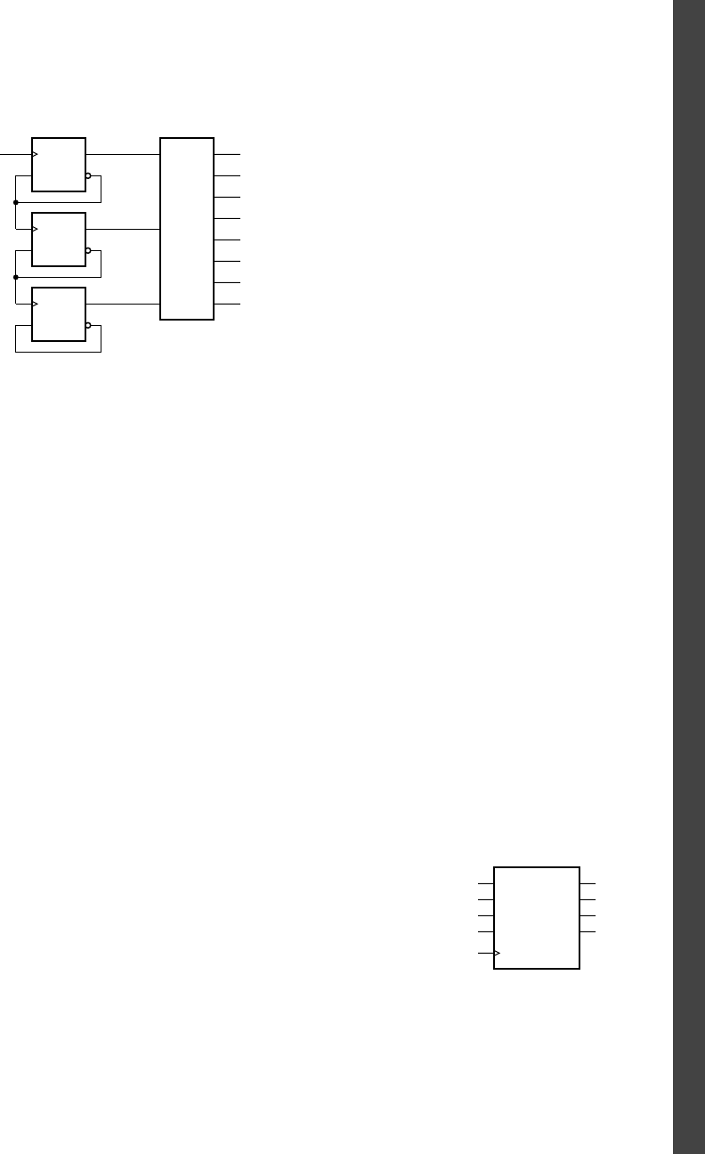
exercise 4.17 Revise the complex multiplier datapath of Example 4.13
to include two fixed-point multiplier components instead of just one. How can
the control sequence described in Example 4.15 be revised as a consequence to
reduce the time taken to perform a complex multiplication?
exercise 4.18 Develop a finite-state machine to implement the revised
control sequence from Exercise 4.17. Show the transition and output functions
both in tabular form and using a state transition diagram.
exercise 4.19 Develop a Verilog model of the complex multiplier as
revised in Exercises 4.17 and 4.18.
exercise 4.20 Identify the control steps required for sequential multipli-
cation using the datapath described in Example 4.4, and develop a finite-state
machine for the control section. Assume that the
x and y operand values are
valid on a cycle when a control signal,
start, is 1. Generate a control signal,
done, that is 1 when when the multiplication is complete. Use a 4-bit counter to
count the successive accumulation steps.
exercise 4.21 Develop a Verilog model of the sequential multiplier in
Exercise 4.20, including both the datapath and the control section.
exercise 4.22 An arbiter is a circuit that allows at most one subsystem
at a time to use a shared resource. A four-way arbiter is shown in Figure 4.48.
Each subsystem sets its request signal to 1 when it wants to use the resource.
When the arbiter sets the grant signal to 1, the subsystem uses the resource. The
subsystem sets its request back to 0 when it has finished, and waits for grant
to be 0 before starting a subsequent request. While a subsystem is granted use
of the resource, other requests must wait, rather than pre-empting the active
subsystem.
a) Develop a FSM for a priority arbiter, in which subsystem 0 has highest
priority and subsystem 3 has least priority. A pending request from a
Exercises CHAPTER FOUR 207
D
Q
Q
D
Q
Q
D
Q
Q
Q0
Y0
Y1
Y2
Y3
Y4
Y5
Y6
Y7
Q1
Q2
clk
3-to-8 decoder
clk
clk
clk
FIGURE 4.47
req3
req2
req1
req0
gnt3
gnt2
gnt1
gnt0
clk
FIGURE 4.48
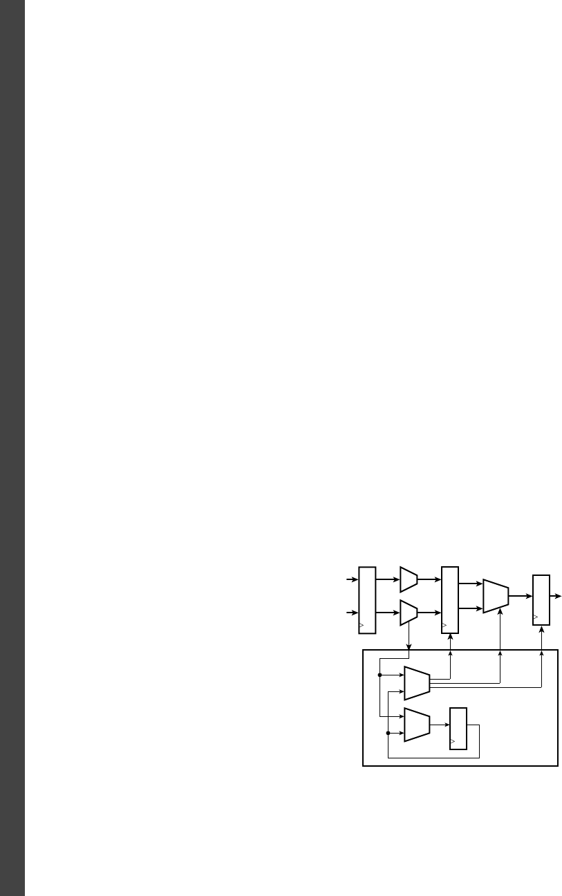
208 CHAPTER FOUR sequential basics
higher-priority subsystem takes precedence over a pending request from a
lower-priority system.
b) Develop a FSM for a round-robin arbiter. Subsystems are granted requests
in order, starting with 0, then 1, 2, 3 and back to 0. A subsystem is skipped
if it has no pending request.
exercise 4.23 Suppose a clocked synchronous system uses registers with
setup time of 150ps and clock-to-output delay of 400ps. Three register-to-
register paths in the datapath have propagation delays of 600ps, 900ps and
1.3ns, respectively.
a) What is the maximum clock frequency at which the datapath can be
operated?
b) If the path with a delay of 1.3ns is optimized to reduce its delay to 800ps,
what is the maximum clock frequency for the optimized datapath?
exercise 4.24 Suppose a clocked synchronous system, in which registers
have setup time of 100ps and clock-to-output delay of 200ps, has a timing con-
straint that the clock frequency be 800MHz. Propagation delays through combi-
national elements in the datapath and control section are shown in Figure 4.49.
The control section uses a Mealy FSM.
a) Identify the critical path in the system.
b) Is the timing constraint on the clock frequency met?
c) If the FSM were changed to be a Moore FSM, would the critical path
change, and would the constraint be met?
150ps
400ps
600ps
350ps
200ps
FIGURE 4.49
exercise 4.25 For a system that operates at a high clock frequency
and samples an asynchronous input that changes with high frequency, the
simple synchronizer of Figure 4.44 may exhibit an unacceptable MTBF.
Equation 4.5 indicates that doubling the sampling delay yields a disproportionate

improvement in MTBF. Design an enhanced synchronizer that samples the input
on alternate rising clock edges.
exercise 4.26 The debouncer circuit of Figure 4.45 uses a “break before
make” switch. What would happen if a “make before break” switch were used?
Such a switch may close the new contact before opening the other contact.
exercise 4.27 Develop a testbench model to verify operation of the
debouncer described in Example 4.20.
exercise 4.28 Develop a testbench model to verify the sequential multi-
plier of Example 4.4 with the control section as described in Exercise 4.20.
Exercises
CHAPTER FOUR 209
This page intentionally left blank
211
memories
Many digital systems use memories for storing information. Memory in
general-purpose computers takes several forms, including semiconductor
memory chips, magnetic disks (hard disks), and optical disks (CDs and
DVDs). In this chapter, we describe the various types of semiconductor
memories, since other forms of memory are much less frequently used
in application-specific digital systems. We start by introducing the gen-
eral concepts that are common to all kinds of semiconductor memory,
and then focus on the particular features of each type. We complete the
chapter with a discussion of techniques for dealing with errors in the
stored data.
5.1 GENERAL CONCEPTS
In Chapter 4 we introduced registers as components for storing binary-
coded information. We generally use separate registers when the number
of items of information to store is small, or when we need to use many
of the items concurrently. When there are numerous items that we can
use one after another, we use memory components instead to store the
information. In this section, we will discuss some of the general concepts
that apply to all kinds of memory components. Then, in the next section,
we will identify some of the specific kinds of memory that are used in
different design scenarios.
A memory is conceptually an array of storage registers, or loca-
tions, each of which has a distinct address, which is a number identifying
the location. Addresses for a memory typically start at 0 and increase
by one for each location, up to one less than the number of locations.
For most memory components, the number of locations is a power of 2.
Thus, a memory with 2
n
locations would have addresses ranging from
0 to 2
n
1, requiring an n-bit address. If each location stores m bits of
encoded information, the total number of bits in the memory component
is 2
n
m.
5
212 CHAPTER FIVE memories
example 5.1 If a memory has 32,768 locations, each of 32 bits, what is
the total capacity of the memory, and how many address bits does it require?
solution The capacity is 1,048,576 bits, that is 2
20
bits. Since
32,768 2
15
, the memory requires 15 address bits.
When referring to memory sizes, we usually use the following multi-
plier prefixes denoting powers of 2:
Kilo (K): 2
10
1,024
Mega (M): 2
20
1,024 2
10
1,048,576
Giga (G): 2
30
1,024 2
20
1,073,741,824
Thus, the memory referred to in Example 5.1 has a capacity of 1M bit.
Note that the multiplier values are close to, but slightly greater than, the
decimal multiplier values with the same names. Note also that we use an
uppercase “K” for the binary multiplier 2
10
, compared with the lowercase
“k” for the decimal multiplier 10
3
. The context of referring to a memory
size is usually assumed to indicate use of the binary multipliers rather than
the decimal multipliers.
Given a memory of a certain capacity, we can organize it in different
ways, varying the number of locations and the number of bits per location.
For example, a 1M bit memory might be organized as a 32K 32-bit
memory, as shown in Example 5.1, or as a 16K 64-bit memory,
64K 16-bit memory, and so on. In practice, the number of locations and
the size of each location are determined by the application requirements,
dictating the memory capacity required.
The two basic operations performed by a memory are writing binary
data to a location and reading the content of a location. For both opera-
tions, we need to provide the address of the location to be written or
read on a set of input signals to the memory component. For a write
operation, we provide the data to write as a further set of input signals,
and for a read operation, the memory component provides the data as
a set of output signals. We control the write operation using control
signals generated by a control section of the digital system that contains
the memory component. We will describe the particular control signals
used by different kinds of memories in a later section. For now, we will
just assume a simple form of memory component with simple control
signals. The input and output signals are shown on a symbol for a mem-
ory component in Figure 5.1. The signal a is the address, encoded as an
unsigned binary number. The signals d_in and d_out carry the data to be
written and the data read, respectively. The encoding for these signals
depends on the application. The control signals are en (enable) and wr
(write). When en is 0, the memory simply maintains all of the stored
왘
왘
왘
a(0)
…
…
a(1)
en
wr
a(n–1)
d_in(0)
…
…
d_in(1)
d_in(m–1)
d_out(0)
…
…
d_out(1)
d_out(m–1)
FIGURE 5.1 Symbol for a
basic memory component.
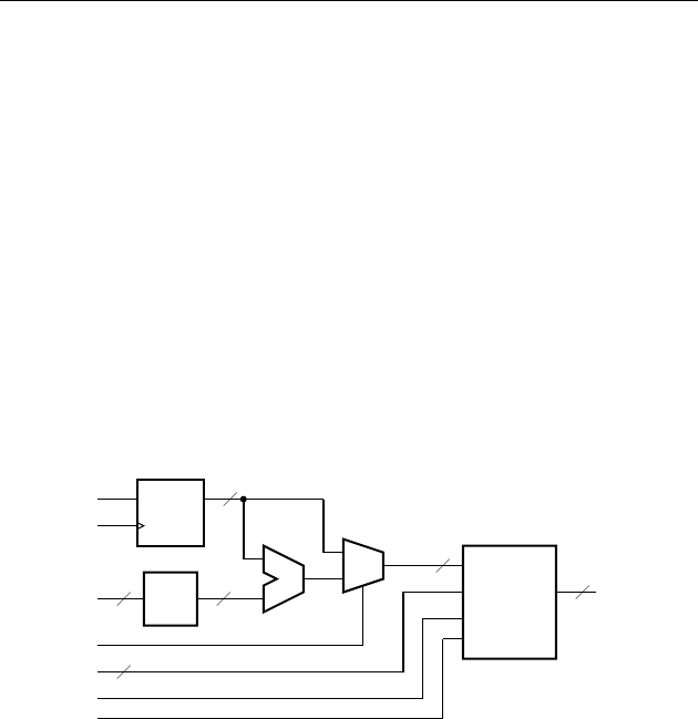
data. When en is 1 and wr is 1, the memory writes data present on the
d_in inputs at the location whose address is present on the a inputs.
When en is 1 and wr is 0, the memory reads the content of the location
whose address is present on the a inputs and drives the data value on
the d_out outputs.
example 5.2 Design an audio echo effects unit that operates by delay-
ing samples of an audio signal represented as a stream of 16-bit 2s-complement
binary-coded values. The sample rate is 50kHz. Arrival of a new input sample
is indicated by a control input,
audio_in_en, being 1 for the clock cycle in which
the sample arrives. The unit should indicate availability of an output sample
using an output control signal,
audio_out_en, in the same way. The delay time is
determined by an 8-bit unsigned input representing the number of milliseconds
of delay. The system clock frequency is 1MHz.
solution We can delay the arriving audio sample values by storing
them in a memory until they are required at the output. The maximum delay
expressed by the 8-bit unsigned input is 255ms. Since samples arrive at a rate of
50kHz (that is, 50 per millisecond), we need to store up to 255 50 12,750
samples. A 16K 16-bit memory, with 14-bit addresses (since 16K 2
14
), will
suffice. A diagram of the datapath including the memory and other components
to compute addresses is shown in Figure 5.2. The figure shows the widths of
each of the multibit signals.
5.1 General Concepts CHAPTER FIVE 213
0
1
a
d_in d_out
en
wr
en Q
×50
–
audio_out
audio_in
delay
clk
count_en
addr_sel
mem_en
mem_wr
8
14
14
14
16
16
clk
FIGURE 5.2 Datapath for an
audio echo effects unit.
We need to use a 14-bit counter to keep track of where samples are stored in the
memory. As each input sample arrives, we store it at the next available memory
location, whose address is given by the counter. We next read from the memory
the value written d milliseconds in the past (where d is the value of the
delay
input) and provide it at the output, then increment the counter to refer to the
next location in memory. This behavior is illustrated in the timing diagram of
Figure 5.3. The value written d milliseconds previously is stored 50 d locations
prior to the current location given by the address counter. Thus, we can compute
its address by multiplying d by 50 and subtracting the result from the value of
the address counter. The counter will increment to the maximum address value
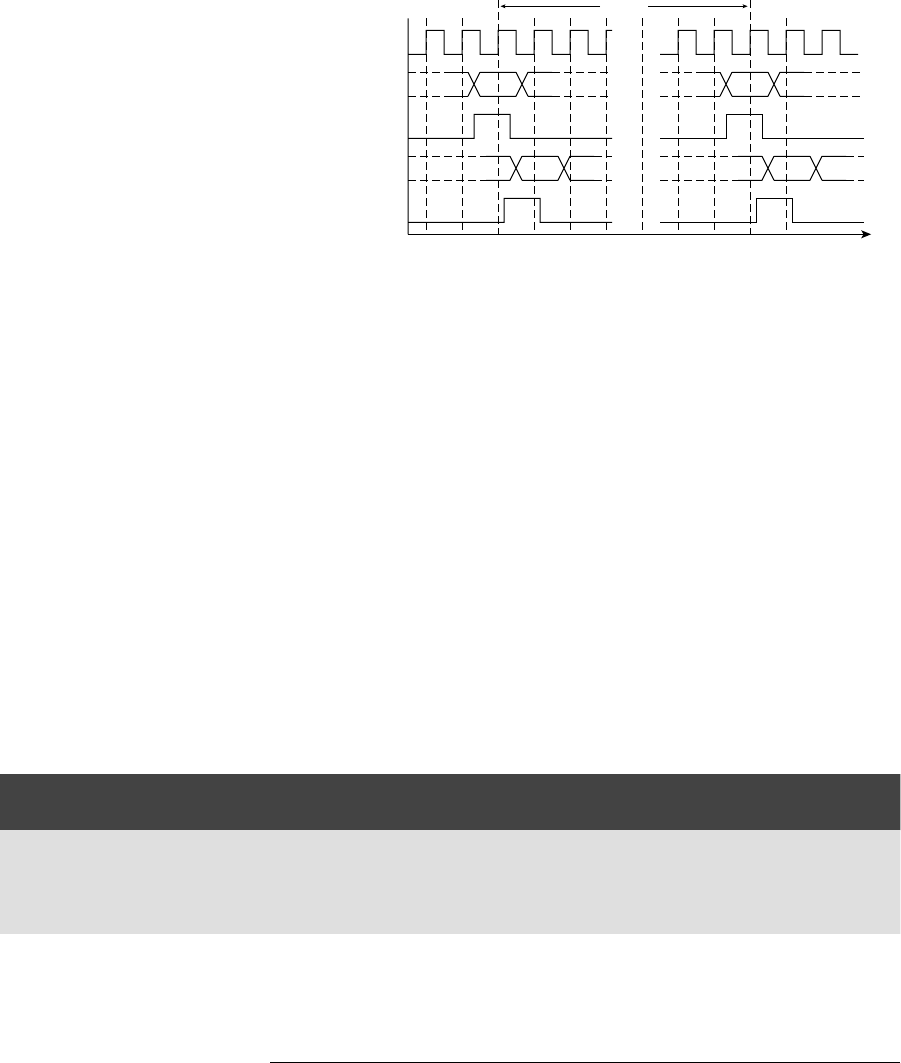
214 CHAPTER FIVE memories
then wrap around to 0, effectively incrementing modulo 16K. Thus, once the
memory is filled, old locations will be overwritten with newly arriving samples.
However, they will have been written more than the maximum delay in the
past, so they will no longer be needed. When we perform the subtraction, we
can ignore the borrow output of the subtracter. The subtracter will yield the
difference modulo 16K, and so give the correct address of the required delayed
sample.
The control sequence for the unit involves two steps:
1. When a sample arrives (indicated by
audio_in_en being 1), set the
multiplexer to use the counter value as the memory address and enable
the memory to perform a write.
2. Set the multiplexer to use the subtracter output as the memory address,
enable the memory to perform a read, set
audio_out_en to 1, and enable
the counter to increment on the next clock edge.
We can use step 1 as the idle state for a state machine that controls this
sequence, provided we use the
audio_in_en signal to gate the write control signal
to the memory. The transition and output functions are specified in Table 5.1.
20µs
s
t
s
t−d
s
t+1
s
t−d+1
clk
audio_in
audio_in_en
audio_out
audio_out_en
FIGURE 5.3 Timing diagram
for the audio echo effects unit.
state
audio_in_en
next
state
addr_sel mem_en mem_wr count_en audio_out_
en
step 1 0 step 1 00000
step 1 1 step 2 01100
step 2 – step 1 11011
TABLE 5.1 Transition and
output functions for the echo unit
control section.
The mem_en and mem_wr signals are Mealy-style outputs, since they depend on
both the state and the
audio_in_en input, whereas the remaining control signals
are all Moore-style outputs.
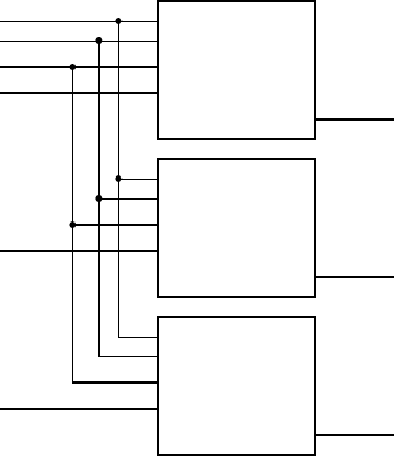
a(13…0)
en
wr
d_in(15…0)
d_out(15…0)
a(13…0)
en
wr
d_in(15…0)
d_out(15…0)
a(13…0)
en
wr
d_in(15…0)
d_out(15…0)
d_out(31…16)
d_out(47…32)
d_out(15…0)
d_in(31…16)
d_in(47…32)
d_in(15…0)
a(13…0)
en
wr
FIGURE 5.4 Connection of
memory components in parallel to
form a wider memory.
5.1 General Concepts
CHAPTER FIVE 215
Manufacturers provide semiconductor memory components in a range
of capacities, varying from a few Kbits through several Mbits and, at time
of writing, up to 2G bits for separately package memory components. Typ-
ically, for a given capacity, a manufacturer provides components organized
with differing widths (1, 4, 8 or 16 bits per location). If an application for
which we are designing a system needs a memory of some other width, we
need to use a number of memory components in parallel. For example, if
we need a 16K 48-bit memory for an application, we could construct
it using three 16K 16-bit memory components. We would connect the
address and control signals together, as shown in Figure 5.4, and use the
data input and output signals of each component for a slice of the overall
data input and output signals.
Connecting multiple memory components together to construct a
memory with more locations is somewhat more involved. We need to
partition the total number of locations among the memory components.
For each read and write operation we need to arrange for the component
containing the required location to perform the operation, and for other
components to remain passive. In many applications, the total number
of locations is a power of 2, say 2
n
, and each memory component has
a smaller number of locations, 2
k
. The number of memory components
is 2
n
/2
k
. The simplest approach to partitioning is to place the first 2
k
locations in the first component, the second 2
k
in the second component,
and so on. If we number the individual memory components 0, 1, 2, and
so on up to (2
n
/2
k
) 1, the component containing a location with address
A is ⎣A/2
k
⎦. This is represented by the most significant n k bits of the
216 CHAPTER FIVE memories
address. We can decode these bits to derive select signals to activate
the required memory component. The address of the location A within
the selected memory component is A mod 2
k
. This is represented by the
least significant k bits of the address. We simply connect these bits of
the address to each of the memory components. The data input signals
are also connected to each of the memory components. The data output
signals need to be driven by the memory component that is selected, so we
use a multiplexer to choose the appropriate data value based on the most
significant address bits.
example 5.3 Design a 64K 8-bit composite memory using four
16K 8-bit components.
solution The complete composite memory is shown in Figure 5.5.
Address bits 15 and 14 are decoded to select which of the four memory com-
ponents is enabled for read and write operations. Those bits also control the
multiplexer to select the output data from the enabled component during a read
operation.
a(13…0)
en
wr
d_in(7…0)
d_out(7…0)
a(13…0)
en
wr
d_in(7…0)
d_out(7…0)
a(13…0)
en
wr
d_in(7…0)
d_out(7…0)
a(13…0)
en
wr
d_in(7…0)
d_out(7…0)
d_out(7…0)
d_in(7…0)
a(13…0)
a(15…14)
en
wr
0
1
2
3
0
en
1
2
3
FIGURE 5.5 Connection of
four 16K 8-bit memory compo-
nents to construct a 64K 8-bit
memory.
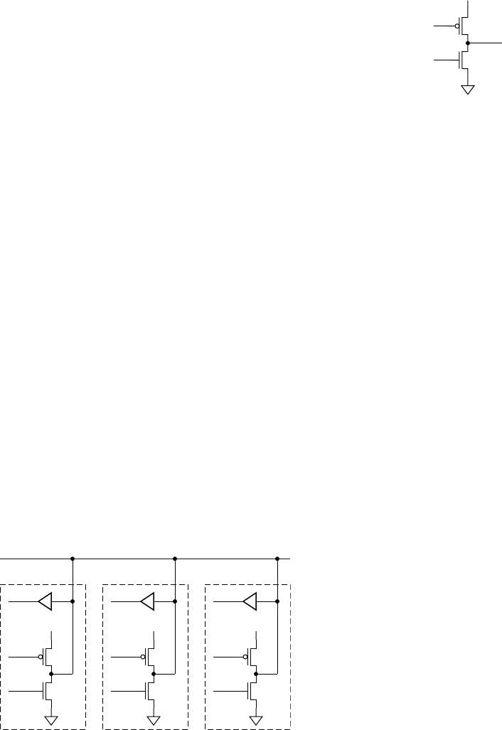
Many manufacturers simplify the connection of memory components
to form larger memories by using a special kind of output driver, called a
tristate driver, for each of the data outputs. Tristate drivers are also used
for buses that allow multiple data sources to provide data in a system. We
will discuss tristate and other bus structures in more detail in Chapter 8 as
part of our discussion of embedded computer systems. For now, we will
focus on their use in memory components.
Unlike ordinary component outputs, which always drive either a low
or high logic level, the output of a tristate driver can be turned off by
placing it in a high-impedance, or hi-Z, state. (“Z” is commonly used as
the symbol for impedance in a circuit.) Thus, a tristate driver has three
output states: logic low, logic high and high impedance; hence the name.
The output circuit of a CMOS digital component involves two transistor
switches as shown in Figure 5.6. To drive the output with a low logic
level, the component turns the bottom transistor on and the top transistor
off, and to drive a high logic level, the component turns the top transistor
on and the bottom transistor off. A tristate driver has the same output
stage, but can turn both transistors off, effectively isolating the compo-
nent from the output.
If we use memory components with tristate data outputs to construct
a larger memory, we can omit the output multiplexer shown in Figure 5.5.
Instead, we simply connect the data outputs of the memory components
together. When a read operation is performed, only the selected memory
component enables its data outputs; all of the disabled components leave
their outputs in the high-impedance state.
Many memory components that have tristate data outputs also combine
the data inputs and outputs into a single set of bidirectional connections,
illustrated in Figure 5.7. This allows a composite memory to be constructed
as shown in Figure 5.8. For memory components implemented as separate
integrated circuits for use on printed circuit boards, the use of bidirectional
connections results in significant cost savings, since there are fewer package
output
+V
FIGURE 5.6 Output stage
circuit.
+V +V +V
FIGURE 5.7 Bidirectional
tristate data connections.
5.1 General Concepts
CHAPTER FIVE 217
218 CHAPTER FIVE memories
pins and interconnecting wires. As we shall see when we study embedded
processors in more detail, this type of memory works well as part of an
embedded computer system, since memory write and read operations are
performed independently. When we perform a write operation, we drive the
data signals with the data to be written. The selected memory component
treats the data connections as inputs and accepts the data to be written. It
keeps its tristate drivers disabled so as not to interfere with the logic levels
in the data signals. When we perform a read operation, we ensure that all
other drivers connected to the data signals are in the high-impedance state
and allow the selected memory component to enable its tristate drivers. It
drives the data signals with the data read from memory.
Of course, whether we can use tristate data connections in a memory
depends on whether the implementation fabric provides them. Memory
components implemented as packaged integrated circuits, for use in a
larger system implemented on a printed circuit board, typically do have
tristate data outputs or tristate bidirectional data input/outputs. On the
other hand, memory blocks provided within ASICs and FPGAs typically
do not have tristate data connections, since tristate buses present some
design and verification challenges in those fabrics. (We will return to
this in Chapter 8.) Instead, data from individual memory blocks must be
combined using multiplexers.
In this section, we have looked at ways of connecting multiple mem-
ory components together to form a memory with wider or more storage
a(13…0)
en
wr
d(7…0)
a(13…0)
en
wr
d(7…0)
a(13…0)
en
wr
d(7…0)
a(13…0)
en
wr
d(7…0)d(7…0)
a(13…0)
a(15…14)
en
wr
0
en
1
2
3
FIGURE 5.8 A composite
memory constructed using
components with common data
inputs and outputs.
locations than provided by a single chip. In each of these schemes, the
memory performs just one operation at a time. In high performance sys-
tems, we can connect multiple memory components together in ways that
permit multiple operations to proceed concurrently, thus increasing the
total number of operations completed per second. These schemes usually
involve organizing the memory into a number of banks, each of which can
perform an operation in parallel with other banks. Successive addresses
are assigned to different banks, since, in many systems, locations are
often accessed in order. As an example, a system with four banks would
assign locations 0, 4, 8, . . . to bank 0; locations 1, 5, 9, . . . to bank 1; 2,
6, 10, . . . to bank 2; and 3, 7, 11, . . . to bank 3. When a read operation is
required for location 4, bank 0 would read that location. Moreover, the
other banks would start a read, prefetching locations 5, 6 and 7. By the
time a read operation is required for these locations (assuming access in
order), the data would already be available from the memory. We will
not describe these advanced memory organizations in any further detail
in this book. Books on computer organization, particularly those con-
centrating on high-performance computers, are a good source of further
information. (See Section 5.5, Further Reading.)
1. What is the capacity in bits of a memory with 4096 locations, each
of 24 bits? How many address bits are required?
2. What is the effect of a write operation? What is the effect of a read
operation?
3. How would we connect four 256M 4-bit memory components to
make a 256M 16-bit memory?
4. How would we connect four 256M 8-bit memory components to
make a 1G 8-bit memory?
5. Which memory component in Question 4 would contain the
location with address 5FC0000
16
?
6. What are the three states of a tristate driver?
7. How do memory components with tristate data outputs simplify
construction of large memories?
5.2 MEMORY TYPES
In this section, we will introduce the various types of memory provided
by manufacturers, either as individual integrated circuits or as resources
within ASIC or FPGA fabrics. We will discuss the distinguishing properties
of each kind of memory, including their timing characteristics and costs,
KNOWLEDGE
TEST QUIZ
KNOWLEDGE
TEST QUIZ
5.2 Memory Types CHAPTER FIVE 219
220 CHAPTER FIVE memories
and describe how to model some of them in Verilog. We will distinguish
between memory that can be both read and written, called random access
memory (RAM), and memory that can only be read, called read-only
memory (ROM). We use the term RAM instead of read/write memory
largely for historical reasons. Memories in very early computers enforced
sequential access, that is, access to locations in increasing order of address,
due to the physical medium on which the data was stored. The invention
of memories in which locations could be read and written with equal facil-
ity in any order (that is, randomly) was a significant milestone, and so the
term RAM has stuck.
5.2.1 ASYNCHRONOUS STATIC RAM
One of the simplest forms of memory is asynchronous static RAM. It is
asynchronous because it does not rely on a clock for its timing. The term
static means that the stored data persists indefinitely so long as power is
applied to the memory component. Compare this with dynamic RAM,
which we will describe later and which loses stored data if it is not peri-
odically rewritten. Static RAM is volatile, meaning that it requires power
to maintain the stored data, and loses data if power is removed. Since
engineers are fond of abbreviations, the term static RAM is usually further
shortened to SRAM.
Asynchronous SRAM internally uses 1-bit storage cells that are similar
to the D-latch circuit that we described in Chapter 4. Within the memory
component, the address is decoded to select a particular group of cells
that comprise one location. For a write operation, the selected latch cells
are enabled and the input data is stored. For a read operation, the address
activates a multiplexer that routes the outputs of the selected latch cells to
the data outputs of the memory component.
The external interface of an asynchronous SRAM is very close to our
general description of a memory component in Section 5.1. For largely
historical reasons, most manufacturers use active-low logic for the control
signals. Further, since asynchronous SRAMs are usually only available
as packaged integrated circuits, and not as blocks in ASIC libraries or
FPGAs, they usually have bidirectional tristate data input/output pins.
Figure 5.9 shows a symbol for a typical asynchronous SRAM. The address
input and the data input/output are as we described in Section 5.1. The
chip-enable input (
__
CE ) is used to enable or disable the memory chip. We
usually drive this input from a select control signal, for example, from an
address decoder in a composite memory. The write-enable input
(
__
WE ) con-
trols whether the memory, if enabled, performs a write or read operation.
The output-enable input (
__
OE ) controls the tristate data drivers during a
read operation. When
__
OE is low during a read, the drivers are enabled and
can drive the read data onto the data pins. When
__
OE is high, the drivers
are in the high-impedance state.
A
CE
WE
OE
D
FIGURE 5.9 Symbol for an
asynchronous SRAM.
Given that the storage cells in an asynchronous SRAM are basically
latches, it is not surprising that the timing is similar to that of a D-latch.
The sequencing of signals to perform a write operation is shown at the left
of Figure 5.10. The control section that sequences the datapath contain-
ing the memory must ensure that the address is stable before commencing
the write operation and is held stable during the entire operation. Oth-
erwise, locations other than the one to be updated may be affected. The
control section selects the particular memory chip by driving
__
CE low, acti-
vates the write operation by driving
__
WE low, and ensures that the chip’s
tristate drivers are disabled by driving
__
OE high. It also sets control signals
to the datapath to provide data on the data signals. The data is stored
transparently in the latch cells for the addressed location. The final data
to be stored must be stable on the data signals a setup time before the
rising edge of the
__
WE signal or the
__
CE signal, whichever occurs first. The
data and the address must also remain stable for a hold time after the
__
WE
or
__
CE signal goes high.
The typical sequencing of signals for a read operation is similar, and
is shown at the right of Figure 5.10. The difference is that the
__
WE signal
is held high, and the
__
OE signal is driven low to enable the memory chip’s
tristate drivers. While this sequence is typical for a read operation done
in isolation, we can also perform back-to-back read operations simply
by changing the address value. The read operation is essentially a combi-
national operation, involving decoding the address and multiplexing the
selected latch-cell’s value onto the data outputs. Changing the address
simply causes a different cell’s value to appear on the outputs after a prop-
agation delay.
Manufacturers of asynchronous SRAM chips publish the timing
parameters for write and read operations in data sheets. The parameters
typically include setup and hold times for address and data values, and
delays for turning tristate drivers on and off. One of the figures of merit of
a memory chip is its access time, which is the delay from the start of a read
WE
OE
CE
A
D
stored data
t
su
t
h
read data
FIGURE 5.10 Timing for
write and read operations in an
asynchronous SRAM.
5.2 Memory Types
CHAPTER FIVE 221
222 CHAPTER FIVE memories
operation to having valid data at the outputs. Other performance-related
parameters are the write cycle time and the read cycle time, which are the
times taken to complete write and read operations, respectively. Manufac-
turers offer chips in different speed grades, with faster chips usually costing
more. This allows us, as designers, to make cost/performance trade-offs in
our designs.
While asynchronous SRAMs are conceptually simple and have simple
timing behavior, the fact that they are asynchronous can make them dif-
ficult to use in clocked synchronous systems. The need to set up and hold
address and data values before and after activation of the control signals
and to keep the values stable during the entire cycle means that we must
either perform operations over multiple clock cycles, or use delay ele-
ments to ensure correct timing within a clock cycle. The former approach
reduces performance, and the latter approach violates assumptions inher-
ent in the clocked synchronous methodology, and so complicates timing
design and analysis. For these reasons, asynchronous SRAMs are usually
used only in systems with low performance requirements, where their low
cost is a benefit.
5.2.2 SYNCHRONOUS STATIC RAM
Given the difficulties associated with asynchronous SRAMs, many mem-
ory component vendors and implementation fabrics provide synchronous
SRAMs, otherwise known as SSRAMs. The internal storage cells of
SSRAMs are the same as those of asynchronous SRAMs. However, the
interface includes clocked registers for storing the address, input data
and control signal values, and in some cases, output data. In this section,
we will describe two forms of SSRAMs in general terms. The details of
control signals and timing will vary between SSRAMs provided by dif-
ferent component vendors and implementation fabrics. As always, we
need to read and understand the data sheets before using a component
in a design.
The simplest kind of SSRAM is often called a flow-through SSRAM.
It includes registers on the inputs, but not on the data outputs. The term
flow-through refers to the fact that data read from the memory cells flows
through directly to the data outputs. Having registers on the inputs allows
us to generate the address, data and control signal values according to our
clocked synchronous design methodology, ensuring that they are stable in
time for a clock edge. Figure 5.11 illustrates the timing for a flow-through
SSRAM. During the first clock cycle, we set up the address (a
1
), control
signals and input data (xx) in preparation for a write operation. These
values are stored in the input registers on the next clock edge, causing the
SSRAM to start the write operation. The data is stored and flows through
to the output during the second clock cycle. While that happens, we set up
the address (a
2
) and control signals in preparation for a read operation.
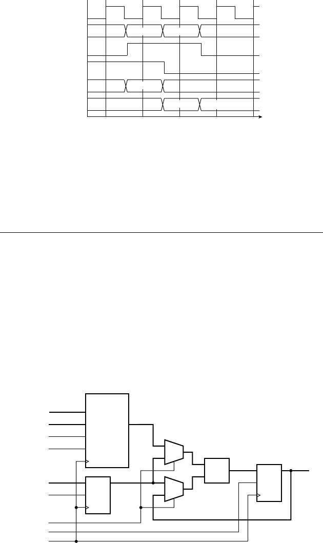
Again, these values are stored on the next clock edge, and during the
third cycle the SSRAM performs the read operation. The data, denoted
by M(a
2
), flows through from the memory to the output. Now, in the
third cycle, we set the enable signal to 0. This prevents the input registers
from being updated on the next clock edge, so the previously read data is
maintained at the output.
example 5.4 Design a circuit that computes the function y c
i
x
2
,
where x is a binary-coded input value and c
i
is a coeffi cient stored in a
fl ow-through SSRAM. x, c
i
and y are all signed fi xed-point values with 8 pre-
binary-point and 12 post-binary-point bits. The index i is also an input to the
circuit, encoded as a 12-bit unsigned integer. Values for x and i arrive at the
input during the cycle when a control input, start, is 1. The circuit should mini-
mize area by using a single multiplier to multiply c
i
by x and then by x again.
solution A datapath for the circuit is shown in Figure 5.12. The 4K
20-bit flow-through SSRAM stores the coefficients. A computation starts with
the index value,
i, being stored in the SSRAM address register, and the data
clk
A
en
wr
D_in
D_out
a
1
xx
xx M(a
2
)
a
2
FIGURE 5.11 Timing for a
fl ow-through SSRAM.
D_in
A
SSRAM
en
wr
D_out
D
ce
Q
D
ce
Q
×y
i
c_in
c_ram_wr
x_ce
c_ram_en
x
y_ce
mult_sel
clk
0
1
0
1
clk
clk
clk
FIGURE 5.12 Datapath for a
circuit to multiply the square of an
input by an indexed coeffi cient.
5.2 Memory Types
CHAPTER FIVE 223
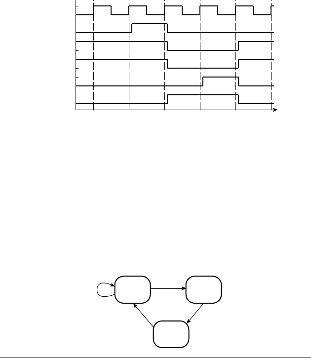
224 CHAPTER FIVE memories
input, x, being stored in the register shown below the SSRAM. On the second
clock cycle, the SSRAM performs a read operation. The coefficient read from
the SSRAM and the stored
x value are multiplied, and the result is stored in the
output register. On the third cycle, the multiplexer select inputs are changed so
that the value in the output register is further multiplied by the stored
x value,
with the result again being stored in the output register.
For the control section, we need to develop a finite state machine that sequences
the control signals. It is helpful to draw a timing diagram showing progress of
the computation in the datapath and when each of the control signals needs to
be activated. The timing diagram is shown in Figure 5.13, and includes state
names for each clock cycle. An FSM transition diagram for the control section is
shown in Figure 5.14. The FSM is a Moore machine, with the outputs shown in
each state in the order
c_ram_en, x_ce, mult_sel and y_ce. In the step1 state, we
maintain
c_ram_en and x_ce at 1 in order to capture input values. When start
changes to 1, we change
c_ram_en and x_ce to 0 and transition to the step2 state
to start computation. The
y_ce control signal is set to 1 to allow the product of
the coefficient read from the SSRAM and the
x value to be stored in the y output
register. In the next cycle, the FSM transitions to the
step3 state, changing the
mult_sel control signal to multiply the intermediate result by the x value again
and storing the final result in the
y output register. The FSM then transitions
back to the
step1 state on the next cycle.
y_ce
c_ram_en
start
clk
step1 step1 step2 step3 step1
x_ce
mult_sel
FIGURE 5.13 Timing
diagram for the computation
circuit.
step1
1, 1, 0, 0
0
1
step2
0, 0, 0, 1
step3
0, 0, 1, 1
FIGURE 5.14 Transition
diagram for the circuit control
section.
clk
A
en
wr
D_in
D_out
a
1
xx
xx M(a
2
)
a
2
FIGURE 5.15 Timing for a
pipelined SSRAM.
Another form of SSRAM is called a pipelined SSRAM. It includes a
register on the data output, as well as registers on the inputs. A pipelined
SSRAM is useful in higher-speed systems where the access time of the
memory is a significant proportion of the clock cycle time. If there is
no time in which to perform combinational operations on the read data
before the next clock edge, it needs to be stored in an output register
and used in the subsequent clock cycle. A pipelined SSRAM provides
that output register. The timing for a pipelined SSRAM is illustrated in
Figure 5.15. Timing for the inputs is the same as that for a flow-through
SSRAM. The difference is that the data output does not reflect the result
of a read or write operation until one clock cycle later, albeit immediately
after the clock edge marking the beginning of that cycle.
example 5.5 Suppose we discover that, in the datapath of Example 5.4,
the combination of the SSRAM access time plus the delays through the
multiplexer and multiplier is too long. This causes the clock frequency to be too
slow to meet our performance constraint. We change the memory from a fl ow-
through to a pipelined SSRAM. How is the circuit design affected?
solution As a consequence of the SSRAM change, the coefficient value is
available at the SSRAM output one cycle later. To accommodate this, we could
insert a cycle into the control sequence to wait for the value to be available.
Rather than wasting this time, we can use it to multiply the value of
x by itself,
and perform the multiplication by the coefficient in the third cycle. This change
requires us to swap the input to the top multiplexer in Figure 5.12, so that it
selects the stored
x value when mult_sel is 0 in state step2 and the SSRAM
output when
mult_sel is 1 in step3. The FSM control sequence is otherwise
unchanged.
Verilog Models of Synchronous Static Memories
In this section, we will describe how to model SSRAMs in such a way that
synthesis CAD tools can infer a RAM and use the appropriate memory
5.2 Memory Types CHAPTER FIVE 225

226 CHAPTER FIVE memories
resources provided in the target implementation fabric. We saw in Chapter 4
that to model a register, we declare a variable to represent the stored regis-
ter value and assign a new value to it on a rising clock edge. We can extend
this approach to model an SSRAM in Verilog. We need to declare a vari-
able that represents all of the locations in the memory. The way to do this
is to declare an array variable, which represents a collection of values, each
with an index that corresponds to its location in the array. For example, to
model a 4K 16-bit memory, we would write the following declaration:
reg [15:0] data_RAM [0:4095];
The declaration specifies a variable named data_RAM that is an array with
elements index from 0 to 4095. Each element is a 16-bit vector.
Once we have declared the variable representing the storage, we write
an always block that performs the write and read operations. The block
is similar in form to that for a register. For example, an always block to
model a flow-through SSRAM based on the variable declaration above is
always @(posedge clk)
if (en)
if (wr) begin
data_RAM[a] <= d_in; d_out <= d_in;
end
else
d_out <= data_RAM[a];
On a rising clock edge, the block checks the enable input, and only per-
forms an operation if it is 1. If the write control input is 1, the block
updates the element of the data_RAM signal indexed by the address using
the data input. The block also assigns the data input to the data output,
representing the flow-through that occurs during a write operation. If the
write control input is 0, the block performs a read operation by assigning
the value of the indexed data_RAM element to the data output.
example 5.6 Develop a Verilog model of the circuit using fl ow-through
SSRAMs, as described in Example 5.4.
solution The module definition includes the address, data and control
ports, as follows:
module scaled_square ( output reg signed [7:-12] y,
input signed [7:-12] c_in, x,
(continued)

input [11:0] i,
input start,
input clk, reset );
wire c_ram_wr;
reg c_ram_en, x_ce, mult_sel, y_ce;
reg signed [7:–12] c_out, x_out;
reg signed [7:–12] c_RAM [0:4095];
reg signed [7:–12] operand1, operand2;
parameter [1:0] step1 = 2'b00, step2 = 2'b01, step3 = 2'b10;
reg [1:0] current_state, next_state;
assign c_ram_wr = 1'b0;
always @(posedge clk) // c RAM – flow through
if (c_ram_en)
if (c_ram_wr) begin
c_RAM[i] <= c_in;
c_out <= c_in;
end
else
c_out <= c_RAM[i];
always @(posedge clk) // y register
if (y_ce) begin
if (!mult_sel) begin
operand1 = c_out;
operand2 = x_out;
end
else begin
operand1 = x_out;
operand2 = y;
end
y <= operand1 * operand2;
end
always @(posedge clk) // State register
...
always @* // Next-state logic
...
always @* begin // Output logic
...
endmodule
5.2 Memory Types
CHAPTER FIVE 227

228 CHAPTER FIVE memories
The module declares nets and variables for the internal datapath connections
and control signals. It declares an array variable to represent the coefficient
memory (
c_RAM). It also declares parameters for the state of the control section
finite-state machine, and variables for the current and next state.
After the declarations, we include always blocks and assignments for the data-
path and control section. We omit the details of the finite-state machine. They
are based on the template we described in Chapter 4, and are available on the
companion website. The first block represents the coefficient SSRAM. It uses
the
i input as its address. The second block represents both the combinational
circuits of the datapath and the output register. If the
y_ce variable is 1, the
register is updated with the value computed by the combinational circuits. We
use intermediate variables to divide the computation into two parts, correspond-
ing to the multiplexers and the multiplier, respectively. Note that we use blocking
assignments to these intermediate variables, rather than nonblocking assign-
ments, since they do not represent outputs of storage registers.
Modeling a pipelined SSRAM in Verilog is somewhat more involved,
as we must represent the internal connection from the memory storage to
the output register and ensure that the pipeline timing is correctly repre-
sented. One approach, extending our previous always block for a 16-bit-
wide memory, is
reg pipelined_en;
reg [15:0] pipelined_d_out;
...
always @(posedge clk) begin
if (pipelined_en) d_out <= pipelined_d_out;
pipelined_en <= en;
if (en)
if (wr) begin
data_RAM[a] <= d_in; pipelined_d_out <= d_in;
end
else
pipelined_d_out <= data_RAM[a];
end
In this block, the variable pipelined_en saves the value of the enable input
on a clock edge so that it can be used on the next clock edge to control
the output register. Similarly, the variable pipelined_d_out saves the value
read or written through the memory on one clock edge for assignment to
the output on the next clock edge if the output register is enabled. Since
there are many minor variations on the general concept of a pipelined
SSRAM, it is difficult to present a general template, especially one that
can be recognized by synthesis tools. A common alternative approach is
to use a CAD tool that generates a memory circuit and a Verilog model of
that circuit. We can then instantiate the generated model as a component
in a larger system.
5.2.3 MULTIPORT MEMORIES
Each of the memories that we have looked at, both in Section 5.1 and
previously in this section, is a single-port memory, with just one port for
writing and reading data. It has only one address input, even though the data
connections may be separated into input and output connections. Thus, a
single-port memory can perform only one access (a write or a read opera-
tion) at a time. In contrast, a multiport memory has multiple address inputs,
with corresponding data inputs and outputs. It can perform as many opera-
tions concurrently as there are address inputs. The most common form of
multiport memory is a dual-port memory, illustrated in Figure 5.16, which
can perform two operations concurrently. (Note that in this context, we are
using the term “port” to refer to a combination of address, data and control
connections used to access a memory, as distinct from a Verilog port.)
A multiport memory typically consumes more circuit area than a
single-port memory with the same number of bits of storage, since it has
separate address decoders and data multiplexers for each access port.
Only the internal storage cells of the memory are shared between the
multiple ports, though additional wiring is needed to connect the cells to
the access ports. However, the cost of the extra circuit area is warranted
in some applications, such as high performance graphics processing and
high-speed network connections. Suppose we have one subsystem produc-
ing data to store in the memory, and another subsystem accessing the data
to process it in some way. If we use a single-port memory, we would need
to multiplex the addresses and input data from the subsystems into the
memory, and we would have to arrange the control sections of the subsys-
tems so that they take turns to access the memory. There are two potential
problems here. First, if the combined rate at which the subsystems need
to move data in and out of the memory exceeds the rate at which a single
access port can operate, the memory becomes a bottleneck. Second, even
if the average rates don’t exceed the capacity of a single access port, if the
two subsystems need to access the memory at the same time, one must
wait, possibly causing it to lose data. Having separate access ports for the
subsystems obviates both of these problems.
The only remaining difficulty is the case of both subsystems accessing
the same memory location at the same time. If both accesses are reads, they
can proceed. If one or both is a write, the effect depends on the characteristics
of the particular dual-port memory. In an asynchronous dual-port memory,
a write operation performed concurrently with a read of the same location
will result in the written data being reflected on the read port after some
delay. Two write operations performed concurrently to the same location
result in an unpredictable value being stored. In the case of a synchronous
D_in1
A1 A2
dual-port
SSRAM
en1
D_in2
D_out1 D_out2
ren2
wr1 wr2
clk1 clk2
FIGURE 5.16 A dual-port
memory.
5.2 Memory Types
CHAPTER FIVE 229

230 CHAPTER FIVE memories
dual-port memory, the effect of concurrent write operations depends on
when the operations are performed internally by the memory. We should
consult the data sheet for the memory component to understand the effect.
Some multiport memories, particularly those manufactured as pack-
aged components, provide additional circuits that compare the addresses on
the access ports and indicate when contention arises. They may also provide
circuits to arbitrate between conflicting accesses, ensuring that one proceeds
only after the other has completed. If we are using multiport memory compo-
nents or circuit blocks that do not provide such features and our application
may result in conflicting accesses, we need to include some form of arbitra-
tion as a separate part of the control section in our design. An alternative is
to ensure that the subsystems accessing the memory through separate ports
always access separate locations, for example, by ensuring that they always
operate on different blocks of data stored in different parts of the memory.
We will discuss block processing of data in more detail in Chapter 9.
example 5.7 Develop a Verilog model of a dual-port, 4K 16-bit fl ow-
through SSRAM. One port allows data to be written and read, while the other
port only allows data to be read.
solution In the following module definition, the clk input is common to
both memory ports. The inputs and outputs with names ending in “1” are the
connections for the read/write memory port, and the inputs and outputs with
names ending in “2” are the connection for the read-only memory port.
module dual_port_SSRAM ( output reg [15:0] d_out1,
input [15:0] d_in1,
input [11:0] a1,
input en1, wr1,
output reg [15:0] d_out2,
input [11:0] a2,
input [11:0] en2,
input clk );
reg [15:0] data_RAM [0:4095];
always @(posedge clk) // read/write port
if (en1)
if (wr1) begin
data_RAM[a1] <= d_in1; d_out1 <= d_in1;
end
else
d_out1 <= data_RAM[a1];
always @(posedge clk) // read-only port
if (en2) d_out2 <= data_RAM[a2];
endmodule

This is much like our earlier model of a flow-through SSRAM, except that
there are two always blocks, one for each memory port. The declaration of the
variable for the memory storage is the same, with the variable being shared
between the two blocks. The block for the read/write port is identical in form to
the block we introduced earlier. The block for the read-only port is a simplified
version, since it does not need to deal with updating the storage variable.
In this model, we make no special provision for the possibility of concurrent write
and read accesses to the same address. During simulation of the model, one or other
block would be activated first. If the block for the read/write port is activated first,
it updates the memory locati
on, and the read operation yields the updated value.
On the other hand, if the block for the read-only port is activated first, it reads the
old value before the location is updated. When the model is synthesized, the syn-
thesis tool chooses a dual-port memory component from its library. The effect of a
concurrent write and read would depend on the behavior of the chosen component.
One specialized form of dual-port memory is a first-in first-out
memory, or FIFO. It is used to queue data arriving from a source to be
processed in order of arrival by another subsystem. The data that is first
in to the FIFO is the first that comes out; hence, the name. The most com-
mon way of building a FIFO is to use a dual-port memory as a circular
buffer for the data storage, with one port accepting data from the source
and the other port reading data to provide to the processing subsystem.
Each port has an address counter to keep track of where data is writ-
ten or read. Data written to the FIFO is stored in successive free loca-
tions. When the write-address counter reaches the last location, it wraps
to location 0. As data is read, the read-address counter is advanced to
the next available location, also wrapping to 0 when the last location is
reached. If the write address wraps around and catches up with the read
address, the FIFO is full and can accept no more data. If the read address
catches up with the write address, the FIFO is empty and can provide no
more data. This scheme is similar to that used for the audio echo effects
unit in Example 5.2, except that the distance between the write and read
addresses is not fixed. Thus, a FIFO can store a variable amount of data,
depending on the rates of writing and reading data. The size of memory
needed in a FIFO depends on the maximum amount by which reading of
data lags writing. Determining the maximum size may be difficult to do.
We may need to evaluate worst-case scenarios for our application using
mathematical or statistical models of data rates or using simulation.
example 5.8 Design a FIFO to store up to 256 data items of 16 bits each,
using a 256 16-bit dual-port SSRAM for the data storage. The FIFO should
provide status outputs, as shown in the symbol in Figure 5.17, to indicate when
the FIFO is empty and full. Assume that the FIFO will not be read when it is
5.2 Memory Types CHAPTER FIVE 231
D_wr
FIFO
wr_en
rd_en
D_rd
empty
reset full
clk
FIGURE 5.17 Symbol for a
FIFO with empty and full status
outputs.
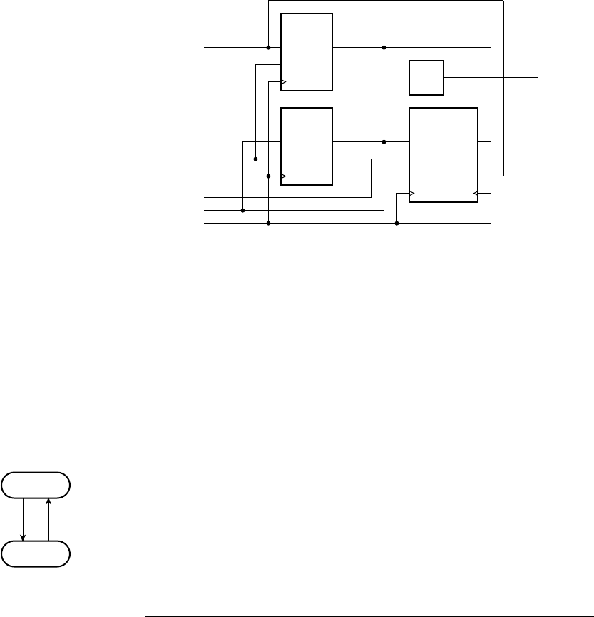
232 CHAPTER FIVE memories
empty, nor be written to when it is full, and that the write and read ports share a
common clock.
solution The datapath for the FIFO, shown in Figure 5.18, uses 8-bit
counters for the write and read addresses. The write address refers to the next
free location in the memory, provided the FIFO is not full. The read address
refers to the next location to be read, provided the FIFO is not empty. Both
counters are cleared to 0 when the
reset signal is active.
D_wr
A_wr A_rd
dual-port
SSRAM
wr_en
D_rd
rd_en
counter
8-bit
ce
reset
Q
counter
8-bit
ce
reset
Q
= equal
A_rd
A_wr
D_rd
clk
wr_en
D_wr
reset
rd_en
clk
clk
clk clk
FIGURE 5.18 Datapath for a
FIFO using a dual-port memory.
The FIFO being empty is indicated by the two address counters having the
same value. The FIFO is full when the write counter wraps around and catches
up with the read counter, in which case the counters have same value again.
So equality of the counters is not sufficient to distinguish between the cases of
the FIFO being empty or full. We could keep track of the number of items in the
FIFO, for example, by using a separate up/down counter to count the number
of items rather than trying to compare the addresses. However, a simpler way
is to keep track of whether the FIFO is filling or emptying. A write operation
without a concurrent read means the FIFO is filling. If the write address becomes
equal to the read address as a consequence of the FIFO filling, the FIFO is full.
A read operation without a concurrent write means the FIFO is emptying. If the
wr
ite address becomes equal to the read address as a consequence of the FIFO
emptying, the FIFO is empty. If a write and a read operation occur concurrently,
the amount of data in the FIFO remains unchanged, so the filling or emptying
state remains unchanged. We can describe this behavior using an FSM, as shown
in Figure 5.19, in which the transitions are labeled with the values of the
wr_en
and
rd_en control signals, respectively. The FSM starts in the emptying state. The
empty status output is 1 if the current state is
emptying and the equal signal is 1,
and the full status output is 1 if the current state is
filling and the equal signal is
1. Note that this control sequence relies on the assumption of a common clock
between the two FIFO ports, since the FSM must have a single clock to operate.
emptying
filling
1, 0 0, 1
FIGURE 5.19 Transition
diagram for the FIFO FSM.
One important use for FIFOs is to pass data between subsystems
operating with different clock frequencies, that is, between different clock
domains. As we discussed in Section 4.4.1, when data arrives asynchro-
nously, we need to resynchronize it with the clock. If the clocks of two
clock domains are not in phase, data arriving at one clock domain from
the other could change at any time with respect to the receiving domain’s
clock, and so must be treated as an asynchronous input. Resynchronizing
the data means passing it through two or more registers. If the sending
domain’s clock is faster than that of the receiving domain, the data being
resynchronized may be overrun by further arriving data. A FIFO allows
us to smooth out the flow of data between the domains. Data arriving is
written into the FIFO synchronously with the sending domain’s clock, and
the receiving domain reads data synchronously with its clock. Control of
such a FIFO is more involved than that for the FIFO with a single clock
illustrated in Example 5.8. The Xilinx Application Note, XAPP 051 (see
Section 5.5, Further Reading) describes a technique that can be used.
FIFOs are also used in applications such as computer networking,
where data arrives from multiple network connections at unpredictable
times and must be processed and forwarded at high speed. Several mem-
ory component vendors provide packaged FIFO circuits that include the
dual-port memory and the address counting and control circuits. Some of
the larger FPGA fabrics also provide FIFO address counting control cir-
cuits that can be used with built-in memory blocks. If we need a FIFO in a
system implemented in other fabrics, we can either design one, as we did
in Example 5.8, or use a FIFO block from a library or a generator tool.
5.2.4 DYNAMIC RAM
Dynamic RAM (DRAM) is another form of volatile memory that
uses a different form of storage cell for storing data. We mentioned
in Section 5.2.1 that static RAM uses storage cells that are similar to
D-latches. In contrast, a storage cell for a dynamic RAM uses a single
capacitor and a single transistor, illustrated in Figure 5.20. The DRAM
cells are thus much smaller than SRAM cells, so we can fit many more
of them on a chip, making the cost per bit of storage lower. However,
the access times of DRAMs are longer than those of SRAMs, and the
complexity of access and control is greater. Thus, there is a trade-off of
cost, performance and complexity against memory capacity. DRAMs are
most commonly used as the main memory in computer systems, since
they satisfy the need for high capacity with relatively low cost. How-
ever, they can also be used in other digital systems. The choice between
SRAM and DRAM depends on the requirements and constraints of each
application.
A DRAM represents a stored 1 or 0 bit in a cell by the presence
or absence of charge on the capacitor. When the transistor is turned
5.2 Memory Types CHAPTER FIVE 233
bit line
word line
FIGURE 5.20 A DRAM
storage cell.
234 CHAPTER FIVE memories
off, the capacitor is isolated from the bit line, thus storing the charge
on the capacitor. To write to the cell, the DRAM control circuit pulls
the bit line high or low and turns on the transistor, thus charging or
discharging the capacitor. To read from the cell, the DRAM control
circuit precharges the bit line to an intermediate level, then turns on
the transistor. As the charges on the capacitor and the bit line equalize,
the voltage on the bit line either increases slightly or decreases slightly,
depending on whether the storage capacitor was charged or discharged.
A sensor detects and amplifies the change, thus determining whether
the cell stored a 1 or a 0. Unfortunately, this process destroys the stored
value in the cell, so the control circuit must then restore the value by
pulling the bit line high or low, as appropriate, before turning off the
transistor. The time taken to complete the restoration is added to the
access time, making the overall read cycle significantly longer than than
that for an SRAM.
Another property of a DRAM cell is that, while the transistor is
turned off, charge leaks from the capacitor. This is the meaning of the term
“dynamic” applied to DRAMs. To compensate, the control circuit must
read and restore the value in each cell in the DRAM before the charge
decays too much. This process is called refreshing the DRAM. DRAM
manufacturers typically specify a period of 64ms between refreshes for
each cell. The cells in a DRAM are typically organized into several rectan-
gular arrays, called banks, and the DRAM control circuit is organized to
refresh one row of each bank at a time. Since the DRAM cannot perform
a normal write or read operation while it is refreshing a row, the refresh
operations must be interleaved between writes and reads. Depending on
the application, it may be possible to refresh all rows in a burst once every
64ms. Alternatively, we may have to refresh one row at a time between
writes and reads, making sure that all rows are refreshed within 64ms.
The important thing is to avoid scheduling a refresh when a write or read
is required and cannot be deferred.
Historically, timing of DRAM control signals used to be asynchronous,
and management of refreshing was performed by control circuits external
to the DRAM chips. More recently, manufacturers changed to synchro-
nous DRAMs (SDRAMs) that use registers on inputs to sample address,
data and control signals on clock edges. This is analogous to the differ-
ence between asynchronous and synchronous SRAMs, and makes it easier
to incorporate DRAMs into systems that use a clocked synchronous tim-
ing methodology. Manufacturers have also incorporated refresh control
circuits into the DRAM chips, also making use of DRAMs easier. Since
applications with very high data transfer rate requirements may be limited
by the relatively slow access times of DRAMs, manufacturers have more
recently incorporated further features to improve performance. These
include the ability to access a burst of data from successive locations

without having to provide the address for each, other than the first, and
the ability to transfer on both rising and falling clock edges (double-data
rate, or DDR, and its successors, DDR2 and DDR3). These features are
mainly motivated by the need to provide high-speed bursts of data in
computer systems, but they can also be of benefit in noncomputer digital
systems.
Because of the relative complexity of controlling DRAMs, we will
not go into detail of the control signals required and their sequencing. For
most implementation fabrics, we can incorporate a DRAM control block
from a library, allowing us to connect external DRAMs to the sequential
circuits in our chip. An example is the SDRAM controller, described in
Xilinx Application Note XAPP134, that allows an FPGA-based system
to connect to and control an external SDRAM memory (see Section 5.5,
Further Reading).
5.2.5 READ-ONLY MEMORIES
The memories that we have looked at so far can both read the stored data
and update it arbitrarily. In contrast, a read-only memory, or ROM, can
only read the stored data. This is useful in cases where the data is constant,
so there is no need to update it. It does, of course, beg the question of how
the constant data is placed in the ROM in the first place. The answer is
that the data is either incorporated into the circuit during its manufacture,
or is programmed into the ROM subsequently. We will describe a number
of kinds of ROM that take one or other of these approaches.
Combinational ROMs
A simple ROM is a combinational circuit that maps from an input address
to a constant data value. We could specify the ROM contents in tabular
form, with a row for each address and an entry showing the data value
for that address. Such a table is essentially a truth table, so we could, in
principle, implement the mapping using the combinational circuit design
techniques we described in Chapter 2. However, ROM circuit structures
are generally much denser than arbitrary gate-based circuits, since each
ROM cell needs at most one transistor. Indeed, for a complex combina-
tional function with multiple outputs, it may be better to use a ROM to
implement the function than a gate-based circuit. For example, a ROM
might be a good candidate for the next-state logic or the output logic of a
complex finite-state machine.
example 5.9
Design a 7-segment decoder with blanking input, as
described in Example 2.16 on page 67, using a ROM.
5.2 Memory Types CHAPTER FIVE 235

236 CHAPTER FIVE memories
solution The decoder has five input bits: four for the BCD code and one
for the blanking control. It has seven output bits: one for each segment. Thus,
we need a 32 7-bit ROM, as shown in Figure 5.21. The contents of the ROM
are given in Table 5.2.
example 5.10 Develop a Verilog model of the 7-segment decoder of
Example 5.9.
solution The module definition is
module seven_seg_decoder ( output reg [7:1] seg,
input [3:0] bcd,
input blank );
always @*
case ({blank, bcd})
5'b00000: seg = 7'b0111111; // 0
5'b00001: seg = 7'b0000110; // 1
5'b00010: seg = 7'b1011011; // 2
5'b00011: seg = 7'b1001111; // 3
5'b00100: seg = 7'b1100110; // 4
5'b00101: seg = 7'b1101101; // 5
5'b00110: seg = 7'b1111101; // 6
5'b00111: seg = 7'b0000111; // 7
5'b01000: seg = 7'b1111111; // 8
5'b01001: seg = 7'b1101111; // 9
5'b01010, 5'b01011,
5'b01100, 5'b01101,
5'b01110, 5'b01111:
seg = 7'b1000000; // "–" for invalid code
default: seg = 7'b0000000; // blank
endcase
endmodule
address content address content
0 0111111 6 1111101
1 0000110 7 0000111
2 1011011 8 1111111
3 1001111 9 1101111
4 1100110 10–15 1000000
5 1101101 16–31 0000000
TABLE 5.2 ROM contents for
the 7-segment decoder.
a
b
c
d
e
f
g
BCD0
BCD1
BCD2
BCD3
blank
A0
A1
A2
A3
A4
D0
D1
D2
D3
D4
D5
D6
FIGURE 5.21 A 32 × 7-bit
ROM used as a 7-segment decoder.

As in Example 2.16, we use a case statement in a combinational always block
to implement a truth-table form of the mapping. In this example, however, we
form the address from the concatenation of the
blank and bcd inputs. The case
statement then specifies the outputs for all possible combinations of value for the
address. A synthesis tool could then infer a ROM to implement the mapping.
In FPGA fabrics that provide SSRAM blocks, we can use an SSRAM
block as a ROM. We simply modify the always-block template for the
memory to omit the part that updates the memory content. We could
include a case statement to determine the data output, as in Example 5.10.
For example,
always @(posedge clk)
if (en)
case (a)
9'h0: d_out <= 20'h00000;
9'h1: d_out <= 20'h0126F;
...
endcase
The content of the memory is loaded into the FPGA as part of its
programming when the system is turned on. Thereafter, since the data
is not updated, it is constant. Note, in passing, that we have used the
Verilog notation for hexadecimal values in this model. The notation 9'h1
means a 9-bit vector zero-extended from the value 1
16
, and the notation
20'h0126F means a 20-bit vector with the value 0126F
16
.
For large ROMs, writing the data directly in the Verilog code like this
is very cumbersome. Fortunately, Verilog provides a way of writing the
data in a separate file that can be loaded into the ROM during simula-
tion or synthesis. We use the $readmemh or $readmemb system task, as
follows:
reg [19:0] data_ROM [0:511];
...
initial $readmemh("rom.data", data_ROM);
always @posedge clk)
if (en)
d_out <= data_ROM[a];
The $readmemh system task expects the content of the named file to be
a sequence of hexadecimal numbers, separated by spaces or line breaks.
Similarly, $readmemb expects the file to contain a sequence of binary
5.2 Memory Types CHAPTER FIVE 237

238 CHAPTER FIVE memories
numbers. Thus, the file rom.data specified in the above example could
contain the data
00000 0126F 017C0 A0018
10009 2667A 30115 00000
Values are read from the file into successive elements of the specified vari-
able until either the end of the file is reached or all elements of the variable
are loaded.
Programmable ROMs
ROMs in which the contents are manufactured into the memory are
suitable for applications where the number of manufactured parts is high
and where we are sure that the contents will not need to change over the
lifetime of the product. In other applications, we would prefer to be able
to revise the ROM contents from time to time, or to use a form of ROM
with lower costs for low-volume production. A programmable ROM
(PROM) meets these requirements. It is manufactured as a separately
packaged chip with no content stored in its memory cells. The memory
contents are programmed into the cells after manufacture, either using a
special programming device before the chip is assembled into a system, or
using special programming circuits when the chip is in the final system.
There are a number of forms of PROMs. Early PROMs used fusible
links to program the memory cells. Once a link was fused, it could not
be replaced, so programming could only be done once. These devices
are now largely obsolete. They were replaced by PROMs that could be
erased, either with ultraviolet light (so called EPROMs), or electrically
using a higher-than-normal power-supply voltage (so-called electrically
erasable PROMs, or EEPROMs).
Flash Memories
Most new designs use flash memory, which is a form of electrically erasable
programmable ROM. It is organized so that blocks of storage can be erased
at once, followed by programming of individual memory locations. A flash
memory typically allows only a limited number of erasure and program-
ming operations, typically hundreds of thousands, before the device “wears
out.” Thus, flash memories are not a suitable replacement for RAMs.
There are two kinds of flash memories, NOR and NAND flash,
referring to the organization of the transistors that make up the memory
cells. Both kinds are organized as blocks (commonly of 16, 64, 128, or
256 Kbytes) that must be erased in whole before being written. In a NOR
flash memory, locations can then be written (once per erasure) and read (an
arbitrary number of times) in random order. The IC has similar address,
data and control signals to an SRAM and can read data with a comparable
access time, making it suitable for use as a program memory for an embed-
ded processor, for storing configuration parameters to be used to control
system operation, and for storing configuration information for FPGAs.
In a NAND flash memory, on the other hand, locations are written
and read one page at a time, a page being typically 2 Kbytes. Read access
to a given location would require reading the page containing the loca-
tion, followed by selection of the required data, taking several microsec-
onds. If all of the locations in a page are required, however, sequential
reading is much faster, comparable in time to SRAM. Erasing a block and
writing a page of data are significantly slower than SRAM access times.
For example, the data sheet for the Micron Technology MT29F16G08FAA
16G bit IC specifies a random read time of 25µs, a sequential read time
of 25ns, a block erase time of 1.5ms, and a page write time of 220µs.
Given their different access behavior, NAND flash memories have a dif-
ferent interface than SRAMs, making control circuits more involved. The
advantage of NAND flash memory is that the density of storage cells is
greater than that of NOR flash. Thus, NAND flash chips are better suited
to applications in which large amounts of data must be stored cheaply.
One of the largest applications of NAND flash memories is in memory
cards for consumer devices such as digital cameras. They are also used in
USB memory sticks for general purpose computers.
1. What is the difference between RAM and ROM?
2. What is meant by the terms volatile and nonvolatile?
3. What is the difference between static and dynamic RAM?
4. What is meant by the access time of a RAM?
5. Why are asynchronous SRAMs diffi cult to use in high-speed clocked
synchronous designs?
6. What is the difference between fl ow-through and pipelined
SSRAMs?
7. What Verilog type is required for a variable to represent memory
storage?
8. What benefi t does a multiport memory have over a single-port
memory with multiplexed address and data connections?
9. How can we work out what will happen if we perform concurrent
writes to a given location in a synchronous dual-port memory?
10. What does FIFO stand for?
11. How does a FIFO facilitate communication of data between clock
domains?
KNOWLEDGE
TEST QUIZ
KNOWLEDGE
TEST QUIZ
5.2 Memory Types CHAPTER FIVE 239
240 CHAPTER FIVE memories
5.3 ERROR DETECTION AND CORRECTION
In most of our discussions, we have assumed that digital circuits store
and process information correctly, though in Section 2.2.2 we did intro-
duce the idea of bit errors and some approaches to dealing with them. Bit
errors can occur in memories from a number of causes. Some errors are
transient, also called soft errors, and involve a bit flip in a memory cell
without a permanent effect on the cell’s capacity to store data. In DRAMs,
soft errors are typically caused by high-energy neutrons generated by
collision of cosmic rays with atoms in the earth’s atmosphere. The neu-
trons collide with silicon atoms in the DRAM chip, leaving a stream of
charge that can disrupt the storage or reading of charge in a DRAM cell.
The frequency of soft-error occurrence, the soft-error rate, depends on the
way in which DRAMs are manufactured and the location in which they
operate. Hence, soft-error rates are highly variable between systems. Soft
errors can also occur in DRAMs and other memories from electrical inter-
ference, the effects of poor physical circuit design and other causes.
Errors that persist in a memory circuit are called hard errors. They
can result from manufacturing defects or from electrical “wear” after pro-
longed use. A memory cell or chip affected by a hard error is no longer
able to store data. A read operation would always yield a 0 or a 1 value,
regardless of the bit value that was previously written.
Given that memories are more susceptible to bit errors than logic
circuits using flip-flops and registers for storage, due to the storage density
and the longevity of data in memories, it is more common to include some
form of error detection in memory circuits than in logic circuits. A com-
mon approach is to use parity, described in Section 2.2.2. Recall that parity
involves counting the number of 1 bits in a code word and setting a parity
bit to 1 or 0 to ensure that the total number of 1 bits is even (if we choose
even parity) or odd (if we choose odd parity). In the case of memories, use of
parity involves adding an extra bit cell to each memory location. When we
write to a location, we compute the parity bit and store it in the extra cell.
When we read a location, we check that the data, together with the parity
bit, have the correct parity. If so, we assume the data is uncorrupted. Other-
wise, we take appropriate action to deal with the error in the stored data.
The problem with using parity to check for errors, as we discussed in
Section 2.2.2, is that it only allows us to detect a single bit flip in a stored
code word. It does not allow us to identify which bit flipped, nor does it
allow us to detect an even number of bit flips. If we could identify the par-
ticular bit that flipped, we could correct the error by flipping the bit back
to its original value, and then continue operating as normal. We could also
write the corrected data back to the memory on the assumption that the
bit flip was a soft error. In order to be able to identify which bit flipped, we
need to consider the invalid code words that result from flipping each bit of
each valid code word. Provided all of those invalid code words are distinct,
we can use the value of the invalid code word to identify the flipped bit.
One scheme for doing this is to use a form of error correcting code
(ECC) known as a Hamming code. We will start with a single-error cor-
recting Hamming code, that is, a code that allows us to correct a single bit
flip within a code word. If our code word has N bits, we need log
2
N 1
additional check bits for the ECC. For example, if we have 8 data bits, we
need 4 check bits, giving a total of 12 bits. The check bits are computed
from the values of the data bits during a write operation, and the entire
ECC word is written to the memory location.
To illustrate how the check bits are computed, we will number the data
bits of an 8-bit code word d
1
through d
8
and the ECC bits e
1
through e
12
.
(Normally, we’ve numbered bits starting from 0, but for this explanation,
it’s more convenient to number all index positions from 1.) The ECC bits
whose indices are powers of 2 are used as check bits, and the remaining
ECC bits are the data bits, in order, as shown in Figure 5.22. If we write
the indices of the ECC bits in binary, the check bit with a 1 in position i of
its index is the exclusive-OR (that is, the parity) of the data ECC bits that
have a 1 in position i of their indices. For example, check bit e
2
(at index
d
1
d
2
d
3
d
4
d
5
d
6
d
7
d
8
e
1
e
2
e
3
e
4
e
5
e
6
e
7
e
8
e
9
e
10
e
11
e
12
FIGURE 5.22 Distribution
of data and check bits within an
ECC word.
5.3 Error Detection and Correction
CHAPTER FIVE 241
0010
2
) is the exclusive-OR of data bits e
3
, e
6
, e
7
, e
10
and e
11
(at indices
0011
2
, 0110
2
, 0111
2
, 1010
2
and 1011
2
). Since each data ECC bit has at
least two 1 bits in its binary index (otherwise it would be a check bit), each
data bit is included in the computation of at least two check bits.
When the memory location is read, again, the entire ECC word is
read. We recompute the values of the check bits from the data ECC bits
and compare them, using a bit-wise exclusive OR, with the check bits read
from memory. If the comparison result is 0000, the recomputed check bits
match the read check bits, so all is well. However, if one of the stored ECC
bits (either a data bit or a check bit) is flipped from the original, the com-
parison result, called the syndrome, will be other than 0000. It turns out
to be the binary index of the ECC bit that has flipped. Thus, we can use
the syndrome value to correct the error by flipping the indexed bit back.
example 5.11 Compute the 12-bit ECC word corresponding to the
8-bit data word 01100001.
solution The check bits are
e
1
e
3
⊕ e
5
⊕ e
7
⊕ e
9
⊕ e
11
d
1
⊕ d
2
⊕ d
4
⊕ d
5
⊕ d
7
1 ⊕ 0 ⊕ 0 ⊕ 0 ⊕ 1 0
e
2
e
3
⊕ e
6
⊕ e
7
⊕ e
10
⊕ e
11
d
1
⊕ d
3
⊕ d
4
⊕ d
6
⊕ d
7
1 ⊕ 0 ⊕ 0 ⊕ 1 ⊕ 1 1
e
4
e
5
⊕ e
6
⊕ e
7
⊕ e
12
d
2
⊕ d
3
⊕ d
4
⊕ d
8
0 ⊕ 0 ⊕ 0 ⊕ 0 0

242 CHAPTER FIVE memories
e
8
e
9
⊕e
10
⊕e
11
⊕e
12
d
5
⊕d
6
⊕d
7
⊕d
8
0 ⊕ 1 ⊕ 1 ⊕ 0 0
Thus the ECC word is 011000000110.
example 5.12 Determine whether there is an error in the ECC word
110111000110, and if so, correct it.
solution The check bits computed from the data bits of the ECC word are
e
1
e
3
⊕e
5
⊕e
7
⊕e
9
⊕e
11
1 ⊕ 0 ⊕ 1 ⊕ 1 ⊕ 1 0
e
2
e
3
⊕e
6
⊕e
7
⊕e
10
⊕e
11
1 ⊕ 0 ⊕ 1 ⊕ 0 ⊕ 1 1
e
4
e
5
⊕e
6
⊕e
7
⊕e
12
0 ⊕ 0 ⊕ 1 ⊕ 1 0
e
8
e
9
⊕e
10
⊕e
11
⊕e
12
1 ⊕ 1 ⊕ 0 ⊕ 1 1
The syndrome is 1010 ⊕ 1010 0000. Thus, there is no error in the read ECC.
example 5.13 Determine whether there is an error in the ECC word
000111000100, and if so, correct it.
solution The check bits computed from the data bits of the ECC word are
e
1
e
3
⊕e
5
⊕e
7
⊕e
9
⊕e
11
1 ⊕ 0 ⊕ 1 ⊕ 1 ⊕ 0 1
e
2
e
3
⊕e
6
⊕e
7
⊕e
10
⊕e
11
1 ⊕ 0 ⊕ 1 ⊕ 0 ⊕ 0 0
e
4
e
5
⊕e
6
⊕e
7
⊕e
12
0 ⊕ 0 ⊕ 1 ⊕ 0 1
e
8
e
9
⊕e
10
⊕e
11
⊕e
12
0 ⊕ 0 ⊕ 0 ⊕ 1 1
The syndrome is 1101 ⊕ 1000 0101. Thus, there is an error in bit e
5
of the
read ECC. That bit should be flipped back from 0 to 1, giving the corrected
ECC word 000111010100.
Note that we have assumed that only one bit of the stored ECC
word could be in error. If two or more bits flip, the checking process may
incorrectly identify a single bit as having flipped, or it may yield an invalid
syndrome. The problem arises from the fact that we have insufficient invalid
code words to distinguish between single-bit errors and double-bit errors.
A simple remedy is to add further check bits. If we add a check bit that is
the exclusive-OR of all of the data bits, the resulting error-checking code
allows us to correct any single-bit error and to detect (but not correct) any
double-bit error. If we assume that errors are independent, the probability
of a double-bit error is very low, so this scheme suffices in many applica-
tions. If extreme reliability and resilience to errors is required, we can
further extend the error-checking code to enable correcting of multiple-bit
errors. The details of how we might do this are beyond the scope of this
book, but are described in Section 5.5, Further Reading.

5.3 Error Detection and Correction CHAPTER FIVE 243
single-bit
correction
double-bit
detection
N
check
bits overhead
check
bits overhead
8 4 50% 5 63%
16 5 31% 6 38%
32 6 19% 7 22%
64 7 11% 8 13%
128 8 6.3% 9 7.0%
256 9 3.5% 10 3.9%
TABLE 5.3 Number of check
bits and relative storage overhead
for single-bit correction and
additional double-bit detection of
errors.
A final consideration in our discussion of error checking and correcting
for memories is the storage overhead required. In our illustration of ECCs
for 8-bit code words, we saw that correcting single-bit errors requires
4 check bits (a 50% overhead) and detecting double-bit errors requires
5 check bits (a 63% overhead). This is clearly a significant storage over-
head, especially when compared to the single parity bit required just to
detect single-bit errors (a 13% overhead). However, we noted that single-
bit correction using Hamming codes needs log
2
N 1 check bits for N bits
of data. Double-bit error detection needs log
2
N 2 check bits. If we pro-
vide checking and correction over longer data words, the relative storage
overhead is less, as shown in Table 5.3. For larger data words, provision of
this form of error detection and correction is increasingly attractive.
There are other, more elaborate, error correction and detection codes that
we can use as alternatives to Hamming codes. However, they also add check
bits to the data, and so require extra storage capacity and extra circuitry to
detect and correct errors. They differ in the storage overhead and the complex-
ity of the additional circuitry, as well as in the number of simultaneous errors
they can deal with. This range of techniques allows us to make design trade-
offs, depending on the reliability requirements and other constraints of our
application. Since Hamming codes are one of the simplest ECCs, they are most
often used in applications requiring moderately high reliability, such as network
server computers. More complex ECCs are used in specialized high-reliability
applications, such as aerospace computers and communications systems.
1. What is the distinction between a soft error and a hard error?
2. What is a common cause of soft errors in DRAMs?
3. What corrective action can we take when a parity error is detected?
4. Using a Hamming code, how many check bits are required for single-
error correction and double-error detection for 4-bit data words?
KNOWLEDGE
TEST QUIZ
KNOWLEDGE
TEST QUIZ

244 CHAPTER FIVE memories
5.4 CHAPTER SUMMARY
A memory contains an array of storage locations, each with a unique
address. A 2
n
m-bit memory has n-bit addresses that run from 0 to
2
n
1.
A write operation stores a data value at a given location. A read
operation yields the data value stored at a given location. Control
signals govern write and read operations.
We can connect multiple memory components in parallel to store
wider data values. We can connect multiple memory components in
banks, with a decoder to select among the banks, to provide more
locations.
Memories with tristate drivers on the data outputs simplify bank
connection. At most one component drives data outputs at a time;
the rest place their outputs in the high-impedance (hi-Z) state.
Volatile memory only retains data for as long as power is applied.
Nonvolatile memory retains data without power. The term RAM
refers to volatile memory that can be written and read with equal
facility in any order. ROM refers to memory that can only be read
once it is manufactured or programmed.
Data in static RAM (SRAM) persists for as long as power is sup-
plied, whereas data in dynamic RAM (DRAM) must be periodically
refreshed. Asynchronous SRAM does not rely on a clock for its tim-
ing. Synchronous SRAM (SSRAM) uses a clock to sample control,
address and data signals, thus simplifying their incorporation into
clocked synchronous systems. SSRAMs include flow-through and
pipelined variants.
The access time is the delay from starting a read operation to having
valid data. The cycle time is the total time taken for a read or write
operation.
Multiport memories allow concurrent operations by different parts
of a digital system. A first-in first-out (FIFO) is a dual-port memory
used as a queue for data. An important use of FIFOs is to pass data
between different clock domains.
A ROM is a combinational circuit that maps from an address to a
data value. It can be used to implement an arbitrary Boolean function.
Programmable ROMs (PROMs) are programmed with data after
manufacture. Flash memories can be erased and reprogrammed
during system operation, and are useful for storing configuration
information.
왘
왘
왘
왘
왘
왘
왘
왘
왘
왘

Atmospheric neutrons and other effects can cause bit errors in data
stored in a memory. The error may be transient (a soft error) or per-
manent (a hard error).
Check bits can be stored along with data to detect and correct errors.
A single parity bit can detect a single-bit error but not a double-bit
error. Error correcting codes, such as Hamming codes, can correct
single-bit errors and detect double-bit errors.
5.5 FURTHER READING
Advanced Semiconductor Memories: Architectures, Designs, and Appli-
cations, Ashok K. Sharma, Wiley-IEEE Press, 2002. Describes a
range of memory devices, including SRAMS, DRAMS and nonvola-
tile memories.
Computer Organization and Design: The Hardware/Software Interface,
David A. Patterson and John L. Hennessy, Morgan Kaufmann
Publishers, 2005. This book contains a chapter on memory system
design for computers, describing how alternative organizations can
improve memory system performance.
Memory Systems: Cache, DRAM, Disk—A Holistic Approach to
Design, Bruce Jacob, Spencer Ng, and David Wang, Morgan
Kaufmann Publishers, 2007. Includes an extensive description of
DRAM technology and its place in computer memory systems. Also
describes error-correcting codes, including Hamming codes and
more elaborate schemes, and the causes and frequency of occur-
rence of memory errors.
Synchronous and Asynchronous FIFO Designs, Peter Alfke, Xilinx
Application Note XAPP051, 1996, http://direct.xilinx.com/bvdocs/
appnotes/xapp051.pdf. Describes a FIFO control scheme for an
FPGA in which the write and read clocks are different.
Synthesizable High-Performance SDRAM Controllers, Xilinx Applica-
tion Note XAPP134, 2005, http://www.xilinx.com/bvdocs/appnotes/
xapp134.pdf. This application note gives an overview of SDRAM
operation and describes a controller subsystem that can be imple-
mented as part of an FPGA-based design.
A Nonvolatile Memory Overview, Jitu J. Makwana and Dieter K.
Schroder, 2004, http://aplawrence.com/Makwana/nonvolmem
.html. Describes the circuit structures and operation of nonvolatile
memory devices.
왘
왘
5.5 Further Reading CHAPTER FIVE 245

246 CHAPTER FIVE memories
exercise 5.1 A system requires storage for 1 second of video from
a camera. The video data consists of 25 frames per second, with each frame
containing 640 480 pixels of 24 bits. How much memory is required?
exercise 5.2 Suppose 8-bit-wide memory ICs that are used to construct
a memory have a read cycle time of 6ns. The application requires data to be
processed at a rate of 400Mbyte/sec. How wide should the memory be to satisfy
the performance requirement?
exercise 5.3 Figure 5.23 shows a symbol for a 512K 8-bit memory
component. Draw a schematic diagram showing connection of these components
to form a 512K 32-bit memory.
exercise 5.4 Draw a schematic diagram showing connection of the
components of Figure 5.23 to form a 1M 8-bit memory.
exercise 5.5 Draw a schematic diagram showing connection of the
components of Figure 5.23 to form a 2M 16-bit memory.
exercise 5.6 Figure 5.24 shows a symbol for a 512K 8-bit memory
component with tristate bidirectional data input/output connections. Draw a
schematic diagram showing connection of these components to form a
2M 16-bit memory.
exercise 5.7 Suppose a datapath connected to an asynchronous SRAM
has control signals
addr_sel to select the memory address and d_out_en to enable
the memory data tristate drivers. The control section generates these control
signals as well as the control signals for the SRAM, as described in Section 5.2.1
and shown in Figure 5.10. Develop a control sequence for a write operation that
ensures that the setup and hold constraints are met. How many clock cycles does
a write operation take using your control sequence?
exercise 5.8 Develop a Verilog model of the circuit described in
Example 5.4 using a flow-through SSRAM.
exercise 5.9 Develop a Verilog model of the revised circuit described in
Example 5.5 using a pipelined SSRAM.
exercise 5.10 Revise the circuit described in Example 5.4 to compute
y c
2
i
x using a flow-through SSRAM.
exercise 5.11 Develop a Verilog model of the revised circuit described in
Exercise 5.10.
exercise 5.12 Revise the circuit described in Examples 5.4 and 5.5 to
compute y c
2
i
x using a pipelined SSRAM.
EXERCISESEXERCISES
a(18…0)
en
wr
d_in(7…0)
d_out(7…0)
FIGURE 5.23
a(18…0)
en
wr
d(7…0)
FIGURE 5.24

exercise 5.13 Develop a Verilog model of the revised circuit described in
Exercise 5.12.
exercise 5.14 Design a circuit that computes the product of two
128-element vectors, a and b; that is, a vector p such that p
i
a
i
b
i
. The
elements of a and b are stored in separate flow-through SSRAMs, and the
result is to be written into a third flow-through SSRAM. Assume that computa-
tion is started by a control signal,
go, being 1 during a clock cycle. An output
control signal,
done, is to be set to 1 during the cycle when the computation is
complete.
exercise 5.15 Develop a Verilog model of the circuit described in
Exercise 5.14.
exercise 5.16 Revise the circuit of Exercise 5.14 to use pipelined
SSRAMs instead of flow-through SSRAMs.
exercise 5.17 Develop a Verilog model of the revised circuit described in
Exercise 5.16.
exercise 5.18 Revise the model of Example 5.7 so that, in the case of
concurrent write and read operations to the same address, the read operation
always yields
a) the original value before the write
b) the value written
exercise 5.19 Revise the model of Example 5.7 to allow writes through
both ports. Use a simulator to observe the effect of concurrent writes to the same
address.
exercise 5.20 Design an arbiter for a dual-port flow-through SSRAM.
For each port, the arbiter provides a
busy signal that indicates the operation on
the port cannot proceed. Concurrent read and write operations proceed with-
out either
busy being activated, provided the addresses are different or both are
reads. For a read and a write occurring at the same address concurrently, the
write proceeds, and the reading port has its
busy signal activated. For two writes
occurring at the same address concurrently, port 1 proceeds and port 2 has its
busy signal activated.
exercise 5.21 Develop a Verilog model of the FIFO described in
Example 5.8.
exercise 5.22 Suppose a system includes a data source that provides a
stream of 16-bit data values and a processing unit that operates on the stream,
Exercises CHAPTER ONE 247
248 CHAPTER FIVE memories
as shown in Figure 5.25. The source provides successive values at irregular inter-
vals, sometimes faster than they can be processed, and sometimes slower. It has
a
ready output that is 1 during a clock cycle when a data item is available. The
clk
ready
data source
d(15…0)
clk
start done
processing unit
d(15…0)
?
FIGURE 5.25
processing unit has a start control input to initiate processing and a done output
that is set to 1 for a cycle when the data item is processed. Show how the source
and processing unit can be connected using the FIFO of Example 5.8, including
any control sequences required. Assume that if the FIFO is full when a new data
item is provided by the source, the data item is dropped from the stream.
exercise 5.23 The data sheet for a Micron Technolog MT48LC128M4A2
512M bit SDRAM describes the device as consisting of four banks, each containing
8,192 rows by 4,096 columns of 4 bits. A refresh operation refreshes a given row
of all four banks at once. Locations must be refreshed every 64ms. What is average
interval between refresh operations? If the cycle time for data accesses is 7.5ns,
what proportion of accesses would conflict with refresh operations?
exercise 5.24 Develop a Verilog model of a 4-bit Gray code to unsigned
binary converter implemented using a combinational ROM. (See Section 3.1.3
on page 116 for details of the Gray code.)
exercise 5.25 Using the Hamming code described in Section 5.3, com-
pute the 12-bit ECC word corresponding to the 8-bit data words 10010110 and
01101001.
exercise 5.26 Using the Hamming code described in Section 5.3, deter-
mine whether there is an error in each of the following ECC words, and if so,
determine the corrected ECC word and the original data value.
a) 100100011010
b) 000110111000
c) 111011011101
exercise 5.27 Draw a diagram, similar to Figure 5.22, showing the dis-
tribution of data and check bits within an ECC word for 16-bit data. Write the
Boolean equations for the check bits.
249
implementation
fabrics
The hardware of a digital system is implemented using integrated circuits
connected together on printed circuit boards. In this chapter, we describe
the range of integrated circuits that are used for digital systems. We also
discuss some of the important characteristics of integrated circuits and
printed circuit boards that give rise to constraints on our designs.
6.1 INTEGRATED CIRCUITS
The history of digital logic circuits predates the invention of integrated
circuits. Early digital systems were constructed using discrete switching
components, such as relays, vacuum tubes, and transistors. However,
the ability to manufacture a complete circuit on the surface of a silicon
wafer brought about a tremendous cost reduction. Invention of the inte-
grated circuit is credited to Jack Kilby at Texas Instruments in 1958. The
techniques were refined by several developers, and the market for ICs
grew rapidly during the 1960s. As digital ICs became commodity parts,
adoption of digital logic circuits became widespread.
It is instructive to review the history of development of digital IC
technology for two reasons. First, we sometimes need to deal with legacy
systems, that is, systems designed some time ago but that are still in opera-
tion and needing maintenance. Where obsolete parts are unavailable, we
need to design replacement circuits to keep the system operating. Hence,
we need to understand the operation of legacy components and the con-
straints under which they operate. Second, we need to realize that circuit
technology is continually evolving. It’s not sufficient for us to learn how to
design using current components, since they will be obsolete at some stage
in the future. Instead, we need to understand technology evolution and
trends, so that we can “future proof” our designs. Understanding history
is important for projecting into the future.
In this section, we will review the history of digital logic components
and survey the components that are available to us now. We will also
6
250 CHAPTER SIX implementation fabrics
consider the trends affecting near-term evolution of these components and
implementation fabrics.
6.1.1 INTEGRATED CIRCUIT MANUFACTURE
Implementation fabrics for digital systems are based on integrated circuits
(ICs), which are manufactured on the surface of a wafer of pure crystalline
silicon using a sequence of photographic and chemical process steps.
A number of identical rectangular ICs are manufactured together, and then
broken apart for individual packaging. Hence, we often use the name sili-
con chip to refer to a piece of a silicon on which an IC is manufactured.
In preparation for chip manufacture, a cylindrical ingot of silicon is
formed (Figure 6.1, left) and then sawn into wafers less than a millimeter
thick and finely polished (Figure 6.1, right). Early wafers were 50mm in
diameter, but, since then, improvements in manufacturing processes have
yielded successively larger wafer sizes. Now, chips can be manufactured
on 300mm diameter wafers. This allows more chips to be manufactured
at once, and reduces the waste at the edges.
The process of manufacturing a circuit on the wafer surface involves a
number of steps that change the properties of certain areas of the surface
silicon, or add a surface layer of some material in certain areas. There are
several kinds of processing steps that can be applied to selected areas of
the wafer, including
Ion implantation: exposing the surface to a plasma of impurity ions
that diffuse into the silicon, thus altering its electrical properties in
controlled ways.
Etching: chemically eroding an underlying film of material that has
been deposited onto the surface. Films include insulating materials,
such as silicon dioxide; semiconducting materials, such as polycrys-
talline silicon (also known as polysilicon); and conducting materials,
such as aluminum and copper.
왘
왘
FIGURE 6.1 An ingot of
crystalline silicon (left), and sawn
wafers (right).
6.1 Integrated Circuits CHAPTER SIX 251
The key to selecting which areas are affected is photolithography,
which means using a photographic process to draw on the surface (see
Figure 6.2, showing selective etching of a film). The surface is coated with
a thin layer of photoresist, a chemical whose resistance to chemical reac-
tion is changed by exposure to light. The surface is then exposed to light
through a mask that has opaque and transparent areas in the pattern of
features to be drawn. The resist is then developed, dissolving either the
exposed areas or the unexposed areas, depending on the kind of resist.
The areas that are now uncoated can be processed, and then the remain-
ing resist is stripped off.
Manufacturing circuits requires several different masks to form the
circuit layers, as illustrated in Figure 6.3. MOS transistors are formed in
the bottom layers with channel areas containing diffused impurity ions
and gates formed from polysilicon lines. Wiring is formed in higher layers
using etched metal conductors. A complete wafer contains between a few
hundred to a few thousand circuits, depending on the individual circuit
size, as shown in Figure 6.4.
Once the circuits on a wafer have been manufactured, they must be
tested to determine which ones work and which fail due to defects. Small
defects can be introduced into an individual IC by stray particles obscur-
ing light during photolithography, by impurities occurring in chemical
process steps, or by particles impinging on wafers during handling in
the manufacturing process. IC foundries are meticulous in their cleanli-
ness, using chemicals of high purity and operating in special clean rooms.
Nonetheless, stray particles and impurities cannot be completely avoided.
A defect can prevent an IC on a wafer from working. The yield is the
proportion of manufactured ICs that work. Since a whole wafer-lot of
ICs is manufactured together, the cost of the discarded defective ICs must
be amortized over those that work. Larger ICs have an increased chance
of being defective, so it is important for designers to constrain IC area to
reduce cost.
After testing the ICs on a wafer, the wafer is broken into individ-
ual chips, which are then packaged. We will describe the different kinds
(a)
(b)
(c) (d) (e)
wafer
film
resist
mask
FIGURE 6.2 Steps in
photolithographic etching: (a) the
wafer and fi lm coated with resist;
(b) exposure through a photo-
mask; (c) the resist developed;
(d) etching of the underlying fi lm;
(e) the remaining resist stripped.
FIGURE 6.3 Graphical
representation of the layers of an IC.
FIGURE 6.4 A complete
wafer containing multiple ICs.
252 CHAPTER SIX implementation fabrics
of packaging in Section 6.3. Since the packaging process may introduce
further defects, the packaged chips are further tested. They can also be
graded according to maximum operating speed, so that higher perfor-
mance chips can be sold at a premium price.
A number of parameters of the manufacturing process determine
the minimum size of transistors and wires in an IC, and thus the size
of a complete IC. One of the main parameters is the photolithography
resolution, that is, the smallest feature that can accurately be drawn and
processed. Much of the improvement in IC technology is attributable to
advances in photolithography, including use of higher-resolution masks
and shorter wavelengths of light. Reducing the feature size has a number
of benefits. It results in smaller chips for a given function, thus reducing
cost. It allows more circuitry to be placed on a chip of a given size, thus
increasing functionality. It also reduces circuit delays, allowing higher
operating speed. Feature size, along with several other parameters, have
been improving exponentially as manufacturing technology has matured.
Currently, use of extreme ultraviolet light allows us to manufacture circuits
with 90nm feature sizes. Further improvements will allow for 65nm and
smaller sizes. These trends are expected to continue for some time yet. The
publication Exponential Trends in the Integrated Circuit Industry (see
Section 6.6) summarizes the trends.
6.1.2 SSI AND MSI LOGIC FAMILIES
While many early ICs were developed for specific applications, in 1961
Texas Instruments introduced a family of logic components that design-
ers could use as building blocks for larger circuits. Three years later, they
introduced the 5400 and 7400 families of TTL (transistor-transistor logic)
ICs that became the basis of logic design for many years. The 5400 family
components were manufactured for high-reliability military applications,
requiring operation over large temperature ranges, whereas the 7400 fam-
ily components were for commercial and industrial applications. Other
IC manufacturers also provided compatible components, thus making the
7400 family a de facto standard.
The components in the 7400 family are numbered according to the
logic functions they provide. For example, a 7400 component provides
four NAND gates, a 7427 provides three NOR gates, and a 7474 provides
two D flip-flops. Since these components integrate a relatively small num-
ber of circuit elements, they are referred to as small-scale integrated (SSI)
components. As manufacturing techniques improved, larger circuits could
be integrated, leading to what we now call medium-scale integrated (MSI)
components. Examples include the 7490 4-bit counter, and the 7494 4-bit
shift register. The boundary between SSI and MSI is somewhat arbitrary.
For example, it’s not clear whether a 7442 BCD decoder is SSI or MSI.
In addition to extending the range of functions available within the
7400 family, manufacturers developed alternative versions of the com-
ponents with different internal circuitry and correspondingly different
electrical characteristics. One variation reduced the power consumed by
components, at the cost of reduced switching speed. Components in this
family are identified by inclusion of the letter “L” in the part number,
for example, 74L00 and 74L74. Another variation used Schottky diodes
within the internal circuits to reduce switching delays, albeit at the expense
of increased power consumption. These components include the letter
“S” in the part number, for example, 74S00 and 74S74. One of the most
popular variations, the 74LS00 family, combined the lower-power circuits
with Schottky diodes to yield a good compromise between power and
speed. Later variations included the 74F00 “fast” family components and
the 74ALS00 “advanced low-power Schottky” family.
One of the problems with TTL circuits is that they use bipolar tran-
sistors, which have relatively high power consumption even when not
switching. In previous chapters, we have described an alternative circuit
structure, CMOS, which uses field-effect transistors. It was originally
developed around the same time as TTL. One of the earliest CMOS logic
families was the 4000 family, which provided SSI and MSI functions, but
with much lower power consumption. They could also operate over a
much larger power supply range (3V15V), compared to TTL’s nominal
5V, but were much slower and had logic levels that were incompatible
with TTL components. Hence, they did not gain widespread use.
Later, in the 1980s, some manufacturers introduced a new family
of CMOS logic components, the 74HC00 family, that were compatible
with TTL components. They provided the same functionality, but with
lower power consumption and comparable speed. Subsequent variations,
such as the 74AHC00 family, offered improved speed and electrical
characteristics.
One important characteristic of CMOS circuits is that the power
consumption and speed are dependent on the power-supply voltage. By
reducing the voltage, as well as by making the internal circuit features
smaller, speed is increased and power consumption is reduced. These
considerations led the electronics industry to agree on a lower standard
power supply voltage of 3.3V. Manufacturers subsequently developed
component families to operate at the lower voltage with reduced logic
thresholds (74LVC00 family) or with TTL-compatible thresholds
(74LVT00 family). They also developed advanced variations, such as the
74ALVC00 and 74ALVT00 family.
As a result of these evolutionary steps, we now have numerous logic
families from different manufacturers, with an alphabet soup of let-
ters between the “74” prefix and the number that denotes the logic
function. Each family has different trade-offs in power consumption,
6.1 Integrated Circuits CHAPTER SIX 253
254 CHAPTER SIX implementation fabrics
speed and logic-level thresholds. The data books published by the
manufacturers document the characteristics of each family. As design-
ers, we need to understand the power, speed and compatibility con-
straints of an application and choose components from a family that
meets the constraints.
Another aspect of evolution of these families is a change in the
logic functions provided. Early components (generally those with
smaller numbers) provided gates and simple combinational and
sequential functions from which more complex systems could be built.
However, during the 1970s, IC technology developed to the level of
large-scale integration (LSI), at which it became feasible to provide a
small computer, a microprocessor, on a single IC. Embedded systems
using microprocessors became more cost-effective in many applica-
tions than systems constructed from SSI and MSI components. The
7400 family components were then commonly used as glue logic, that
is, simple logic circuits for interconnecting LSI components. As a con-
sequence, new functions added to the later logic families were more
oriented toward glue and interconnection functions, such as multibit
tristate drivers and registers. These more recent components in the
CMOS logic families are the only ones we would consider for new
designs, with older components and TTL families being used only for
maintenance of legacy systems. Programmable logic devices (described
in Section 6.2) and ASICs have almost completely supplanted other
families.
example 6.1 Use the following components to design a 4-digit decimal
counter with a 7-segment LED display: two 74LS390 dual decade counters,
four 74LS47 BCD to 7-segment decoders, four 7-segment displays, plus any
additional gates required.
solution The 74LS390 component contains two counters, each as shown
in Figure 6.5. Internally, the counter consists of a single-bit counter clocked on
the falling edge of
CP0, and a 3-bit divide-by-five counter clocked on the falling
edge of
CP1. A decade (divide-by-ten) counter can be formed by using the single-
bit counter for the least significant bit and connecting the
Q0 output externally
to the
CP1 input. When Q0 changes from 1 to 0, it causes the more significant
bits to count up. The
MR input to the counter is a master reset input. When 1, it
forces the counter outputs to 0000.
We can cascade the 74LS390 decade counters together, using the outputs of each
decade to generate a clock for the next decade. The outputs of a given decade
changing from 1001 (the binary code for 9) to 0000 should cause the next
decade to count up. The only time this occurs is when
Q3 and Q0 of the given
decade both change to 0, so we can use an AND gate to generate the clock for
the next decade, as shown in Figure 6.6.
MR
Q0
Q1
Q2
Q3
CP0
CP1
FIGURE 6.5 A symbol for
each of the decade counters in a
74LS390 component.
MR
Q0
Q1
Q2
Q3
CP0
CP1
MR
Q0
Q1
Q2
Q3
CP0
CP1
MR
Q0
Q1
Q2
Q3
CP0
CP1
MR
Q0
Q1
Q2
Q3
CP0
CP1
The 74LS47 component is shown in Figure 6.7. The inputs A through D are
the BCD value, with
A being the least significant bit and D the most significant
bit. The segment outputs
a through g are active-low, allowing them to drive the
cathodes of a 7-segment display. When the lamp test input,
LT, is low, it turns all
segments on. We can tie it to a high logic level in this application, since we don’t
need to use it. The ripple-blank input (
RBI) and ripple-blank output (RBO) are use
to turn off any leading zero digits in the displayed value. When the
RBI input to
a decoder is low and the BCD value is 0000, all of the segments are turned off
and
RBO is driven low. We tie the RBI input of the most significant digit low, and
chain the
RBO of all digits to the RBI of the next digit (except the least significant
digit, which we always want to display something).
Our complete circuit for the counter with display is shown in Figure 6.8. The
two 74LS390 components are connected as shown in Figure 6.6 using three
AND gates. These gates can be implemented using three of the four AND gates
in a 74LS08 component. Each counter output drives a 74LS47 decoder, which
in turn drives a 7-segment LED display. The resistors are required to limit the
current flowing in each segment LED. The value of the resistor depends on
the required display brightness. Information on current versus brightness can
be found from manufacturer’s data sheets. If we assume 2mA is sufficient,
that the decoder output has a low-level voltage of 0.4V at 2mA, and that the
voltage drop across the segment LED is 1.6V, we need the resistor to drop
5.0
1.6 0.4 3.0V at 2mA. Thus, a 1.5kΩ resistor will suffice.
6.1.3 APPLICATION-SPECIFIC INTEGRATED
CIRCUITS (ASICS)
The developmewnt of IC technology beyond the LSI level led to very large
scale integrated (VLSI) circuits. At that stage, it became clear that the
industry would soon run out of superlatives to prefix to “LSI.” Thus,
the term VLSI came to refer more to the way in which ICs were designed
than the number of transistors they carried. The term now usually means
the detailed circuit design of integrated circuits, as opposed to system-
level design. The widespread availability of CAD tools for VLSI design
and the growth of the IC manufacturing service industry has now made
it practical to develop ICs for a wide range of applications. We use the
term application-specific integrated circuit, or ASIC, to refer to an IC
FIGURE 6.6 Four 74LS390
decade counters cascaded to
make a 4-digit counter.
A
B
C
D
LT
RBI
a
b
c
d
RBO
e
f
g
FIGURE 6.7 A symbol for
the 74LS47 BCD to 7-segment
decoder.
6.1 Integrated Circuits
CHAPTER SIX 255
256 CHAPTER SIX implementation fabrics
manufactured for a particular application. This is not to say that an ASIC
is necessarily manufactured just for one customer or project. Rather, it is
designed to meet a particular set of requirements, and so contains circuits
customized for those requirements. It may be designed for a particular
end product provided by one manufacturer, for example, a portable music
player, a toy, an automobile, a piece of military equipment, or an indus-
trial machine. Alternatively, it may be designed for use in a range of prod-
ucts provided by manufacturers in a particular market segment. These
kinds of ASIC are sometimes called application-specific standard prod-
ucts, or ASSPs, since they are treated as a standard part within the market
MR
Q0
Q1
Q2
Q3
CP0
CP1
MR
Q0
Q1
Q2
Q3
CP0
CP1
A
B
C
D
LT
RBI
a
b
c
d
RBO
e
f
g
A
B
C
D
LT
RBI
a
b
c
d
RBO
e
f
g
MR
Q0
Q1
Q2
Q3
CP0
CP1
A
B
C
D
LT
RBI
a
b
c
d
RBO
e
f
g
MR
Q0
Q1
Q2
Q3
CP0
CP1
A
B
C
D
LT
RBI
a
b
c
d
RBO
e
f
g
CP
MR
+V
+V
+V
+V
+V
+V
+V
+V
FIGURE 6.8 The complete
circuit for the 4-digit counter with
display.
segment, but are not of use outside that segment. Examples include ICs for
cell phones, which are used by a number of competing cell-phone manu-
facturers, but which are not of use in, say, automobile control circuits.
One of the main reasons we would develop an ASIC for a product is
that, being customized for that application, it has lower cost per IC than a
programmable component such as an FPGA (see Section 6.2). However, in
order to achieve that level of customization, we need to invest much more
design and verification effort. We must amortize the non-recurring engineer-
ing (NRE) cost over all of the product units sold. Hence, it only makes sense
to use an ASIC if our product sales volume is sufficiently large. The amortized
NRE cost per unit should be less than the cost difference between an ASIC
and a programmable part. This, of course, assumes that it is feasible to use a
programmable component. If the application requires a level of performance
that cannot be achieved with an FPGA, then an ASIC or an ASSP is our only
real option, and the higher NRE is a necessary part of the product cost.
There are two main design and manufacturing techniques for ASICs,
differing in the degree of customization for the application. We will
describe them briefly in this section, deferring in-depth discussion to
advanced references on VLSI design. First, fully custom integrated circuits
involve detailed design of all of the transistors and connections in an ASIC.
This allows the most effective use of the hardware resources on an IC and
yields higher performance, but has high NRE cost and requires advanced
VLSI design expertise within the design team. As a consequence, fully
custom ASICs are usually only designed for high-volume products, such
as CPUs and ICs for consumer appliances. Second, standard cell ASICs
involve selection of basic cells, such as gates and flip-flops, from a library
to form the circuit. The cells have been previously designed by an IC
manufacturer or an ASIC vendor, and are used by the synthesis tool dur-
ing the design process to implement the design. The value of this approach
is that the NRE cost for each ASIC design is significantly reduced, since
the cost of designing the cell library is amortized over a number of ASIC
designs. The compromise is that the ASIC may not be as dense or have the
performance of a fully custom ASIC.
1. What is photolithography in IC manufacture?
2. How do IC area and defect density on a wafer affect IC cost?
3. What do the “L” and “S” in the part name 74LS47 stand for?
4. What is meant by the term glue logic?
5. What do the terms ASIC and ASSP stand for?
6. Would it make sense to design an ASIC for a customized building
security system to be installed in a new offi ce building? Why (or
why not)?
KNOWLEDGE
TEST QUIZ
KNOWLEDGE
TEST QUIZ
6.1 Integrated Circuits CHAPTER SIX 257
258 CHAPTER SIX implementation fabrics
7. Similarly, would it make sense to design an ASIC for an engine
control system in a car? Why (or why not)?
6.2 PROGRAMMABLE LOGIC DEVICES
The components in SSI and MSI families and ASICs all have fixed func-
tions, determined by the logic circuit for each component. Programmable
logic devices (PLDs), on the other hand, can be programmed after manu-
facture to have different functions. In this section, we will look at the
evolution of PLDs, leading to FPGAs that are in widespread use today.
6.2.1 PROGRAMMABLE ARRAY LOGIC
One of the first successful families of PLDs was introduced in the late
1970s by Monolithic Memories, Inc., and called programmable array
logic (PAL) components. These components were an evolution of earlier
PLDs, but were simpler to use in many applications. A simple representa-
tive component in the family is the PAL16L8, whose circuit is shown in
Figure 6.9. The component has 10 pins that are inputs, 2 pins that are
outputs, and 6 pins that are both inputs and outputs. This gives a total of
16 inputs and 8 outputs (hence the name “16L8”). The symbol at each
input in Figure 6.9 represents a gate that is a combination of a buffer and
an inverter. Thus, the vertical signals carry all of the input signals and
their negations. The area in the dashed box is the programmable AND
array of the PAL. Each horizontal signal in the array represents a p-term
of the inputs, suggested by the AND-gate symbol at the end of the line.
(Recall that a p-term, or product term, is the logical AND of a number
of signals; see Section 2.1.1.) In the unprogrammed state, there is a wire
called a fusible link, or fuse, at each intersection of a vertical and horizon-
tal signal wire, connecting those signal wires. The PAL component can be
programmed by blowing some of the fuses to break their connections, and
leaving other fuses intact. This is done by a special programming instru-
ment before the component is inserted into the final system.
On the diagram of Figure 6.9, we draw an X at the intersection of a
vertical and a horizontal signal to represents an intact fuse. An intersec-
tion without an X means that the intersecting signals are not connected.
So, for example, the horizontal signal numbered 0 has connections to
the vertical signals numbered 24 and 31, which are the signals I8 and
__
I10 . Some of the p-terms are connected to the enable control signals for
the inverting tristate output drivers. Others are connected to the 7-input
OR gates. So, for each output, we can form the AND-OR-INVERT func-
tion of inputs, with up to 7 p-terms involved. In the circuit shown in
Figure 6.9, output
O1 implements the function
_______
I1 · I2 I3 ·
__
I10 , with the
output enabled by the condition I8 ·
__
I10 .
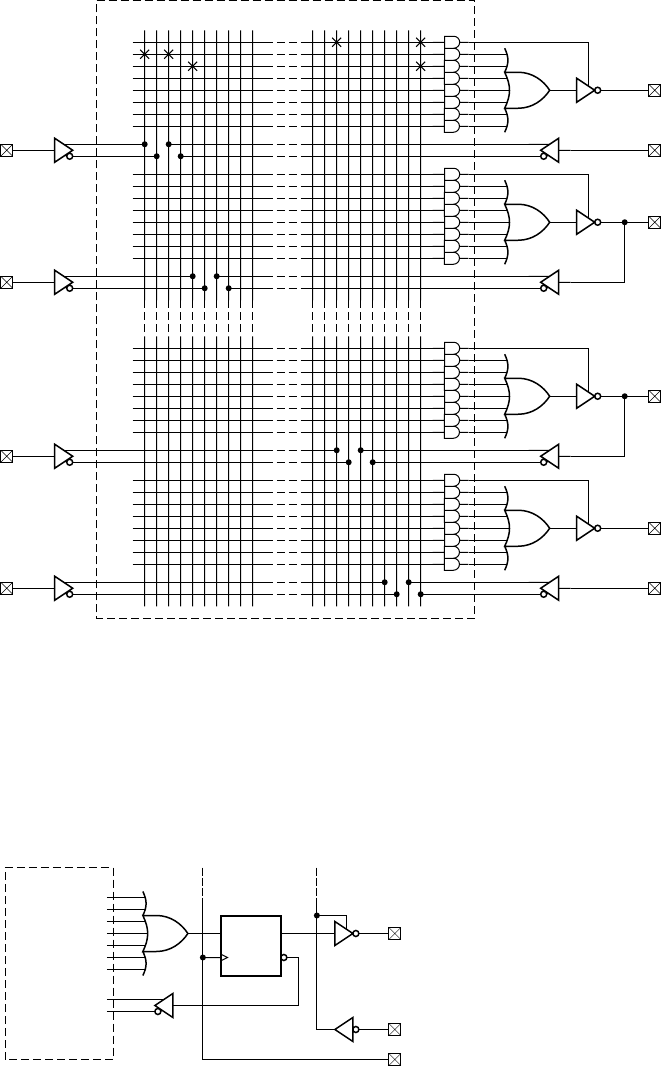
A PAL component such as the PAL16L8 can be programmed to
implement a variety of combinational functions. Other PAL components
also include registers, allowing us to implement simple sequential circuits.
As an example, the output circuit of a PAL16R8 component is shown in
Figure 6.10. The feedback from the register output to the programmable
AND array is useful for implementation of FSMs. Even if a circuit is very
simple, requiring only a handful of gates and flip-flops, there is often
O1
O8
IO2
IO7
I1
I10
I2
I3
…
…
…
…
…
I8
I9
0
0
1
2
3
4
5
6
7
48
49
50
51
52
53
54
55
56
57
58
59
60
61
62
63
8
9
10
11
12
13
14
15
1
2
3
6
7
8
9
4
5
31
30
29
28
27
26
25
24
23
22
FIGURE 6.9 The internal
circuit of a PAL16L8 component.
6.2 Programmable Logic Devices
CHAPTER SIX 259
FIGURE 6.10 Registered
output circuit of a PAL16R8.
DQ
Q
clk
AND
array
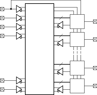
260 CHAPTER SIX implementation fabrics
a benefit in cost and reliability gained from combining several separate
packages into one PAL package. We typically describe the functions to be
implemented in a PAL component in terms of Boolean equations expressed
in an HDL. We then use a synthesis tool to transform the equations into
a gate-level circuit, which we can verify using the same testbench that
we used to verify the Boolean-equation model. Finally, we use physical-
design CAD tools to transform the gate-level model into a fuse map, that
is, a file used by the programming instrument to determine which fuses to
blow. If our functions are too complex to be expressed using the resources
available in a given PAL component, we would either need to use a larger
component, or divide the functions across several components.
As manufacturers developed PLD technology, they found it more
convenient to provide fewer generic components in a family, rather than
a larger number of variants of a given organizational theme. Most of
the variation in earlier families arose in the resources provided for the
outputs, for example, whether outputs were inverting or not, whether
registers were provided, and whether outputs could be fed back as inputs.
In contrast, generic array logic (GAL) components provide output logic
macrocells (OLMCs) that replace the combinations of OR gates, reg-
isters and tristate drivers in PAL output circuits. Each OLMC includes
circuit elements together with programmable multiplexers, allowing
the output functionality to be determined as part of programming the
component. As an example, Figure 6.11 shows the internal circuit orga-
nization of the GAL22V10 component, now manufactured by Lattice
Semiconductor Corporation, and Figure 6.12 shows the OLMC circuit
for each section. The OLMC has p-term inputs from an AND array
with the same organization as that of a PAL component. The number of
p-terms ranges from 8 for some sections to 16 for others. The output of
the OR gate connects to a D flip-flop that has clock, asynchronous reset
8
…
……
OLMC
10
OLMC
10
OLMC
8
OLMC
Programmable
AND array
FIGURE 6.11 Internal circuit
organization of a GAL220V10
component.
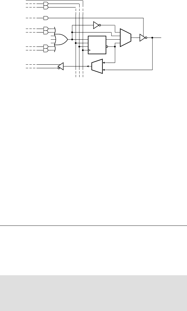
and synchronous preset signals in common with other OLMCs in the
component. The select inputs of the multiplexers are set by programming
the component. The four-input multiplexer allows selection of registered
or combinational output, either inverting or noninverting. The two-input
multiplexer allows either registered or combinational feedback, or, if the
output driver is in the high-impedance state, direct input from the com-
ponent pin. By appropriate programming, a GAL component can emulate
any of the PAL components, including the PAL16L8 and PAL16R8 com-
ponents we have shown here.
In modern designs, we would typically use PLDs such as GAL com-
ponents for simple combinational glue logic, and for relatively simple
sequential circuits. As with PAL components, we would describe the
required functionality in terms of Boolean equations and use a CAD
tool to determine the programming for the component. The circuitry of
the original GAL families was based on similar technology to EPROMs,
allowing them to be programmed, erased using ultraviolet light, and sub-
sequently reprogrammed. Current components can be erased electrically
and programmed in situ in the final circuit.
example 6.2 Design a priority encoder that has 16 inputs, I[0:15]; a
four-bit encoded output,
Z[3:0]; and a valid output that is 1 when any input is 1.
Input
I[0] has the highest priority, and I[15] the lowest priority. The design is to be
implemented in a GAL22V10 component.
solution The Boolean equations for the encoder, expressed in Verilog, are
assign win[0] = I[0];
assign win[1] = I[1] & ~I[0];
assign win[2] = I[2] & ~I[1] & ~I[0];
...
…
D
SP
AR
Q
Q
clk
0
1
2
3
0
1
FIGURE 6.12 Output
logic macrocell of a GAL22V10
component.
6.2 Programmable Logic Devices
CHAPTER SIX 261
(continued)

262 CHAPTER SIX implementation fabrics
assign win[15] = I[15] & ~I[14] & ~I[13] & ... & ~I[0];
assign Z[3] = win[15] | win[14] | win[13] | win[12]
| win[11] | win[10] | win[9] | win[8];
assign Z[2] = win[15] | win[14] | win[13] | win[12]
| win[7] | win[6] | win[5] | win[4];
assign Z[1] = win[15] | win[14] | win[11] | win[10]
| win[7] | win[6] | win[3] | win[2];
assign Z[0] = win[15] | win[13] | win[11] | win[9]
| win[7] | win[5] | win[3] | win[1];
assign valid = I[15] | I[14] | I[13] | ... | I[0];
Each of the win elements can be implemented as a p-term in a row of the GAL
AND array. Each
Z output is thus the OR of 8 p-terms. Since each OLMC in a
GAL22V10 component has at least 8 p-term inputs, these equations will fit in
any of the sections.
The
valid output is the OR of 16 inputs, so it could fit in either of the two sec-
tions that have 16 p-term inputs to the OLMC. However, we can rewrite the
equation for
valid using the DeMorgan law (see Section 2.1.2) as
assign valid ~(~I[15] & ~I[14] & ~I[13] & ... & ~I[0]);
By programming the OLMC for the valid output to negate the OR result, we can
use just one p-term. This allows us to place the
valid output in any section of the
GAL component rather than only in those sections that have 16 OR-gate inputs.
The flexibility afforded by this transformation reduces the constraints on choice
of output pins for the component, and may thus simplify connection of the com-
ponent in a larger circuit.
6.2.2 COMPLEX PLDS
A further evolution of PLDs, tracking advances in integrated circuit tech-
nology, led to the development of so-called complex programmable logic
devices (CPLDs). We can think of a CPLD as incorporating multiple PAL
structures, all interconnected by a programmable network of wires, as
shown in Figure 6.13. (This gives a general idea of CPLD organization.
The actual organization varies between components provided by different
manufacturers.) Each of the PAL structures consists of an AND array and
a number of embedded macrocells (M/Cs in the figure). The macrocells
contain OR gates, mutiplexers and flip-flops, allowing choice among
combinational or registered connections to other elements within the
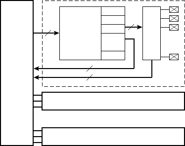
component, with or without logical negation, choice of initialization for
flip-flops, and so on. They are essentially expanded forms of the simple
macrocell shown in Figure 6.12, but without the direct connections to
external pins. Instead, the external pins are connected to an I/O block,
which allows selection among macrocell outputs to drive each pin. The
network interconnecting the PAL structures allows each PAL to use feed-
back connections from other PALs as well as inputs from external pins.
As well as providing more circuit resources than simple PLDs, modern
CPLDs are typically programmed differently. Rather than using EPROM-
like technology, they use SRAM cells to store configuration bits that
control connections in the AND-OR arrays and the select inputs of mul-
tiplexers. Configuration data is stored in nonvolatile flash RAM within
the CPLD chip, and is transferred into the SRAM when power is applied.
Separate pins are provided on the chip for writing to the flash RAM, even
while the chip is connected in the final system. Thus, designs using CPLDs
can be upgraded by reprogramming the configuration information.
Manufacturers provide a range of CPLDs, varying in the number of
internal PAL structures and input/output pins. A large CPLD may contain
the equivalent of tens of thousands of gates and hundreds of flip-flops,
allowing for implementation of quite complex circuits. Whereas it might
be feasible to manually determine the programming for a simple PLD, it
would be quite intractable to do so for a CPLD. Hence, we would use
CAD tools to synthesize a design from an HDL model and to map the
design to the resources provided by a CPLD.
6.2.3 FIELD-PROGRAMMABLE GATE ARRAYS
As we saw in the last section, manufacturers were able to provide larger
programmable implementation fabrics by replicating the basic PAL
structure on a chip. However, there is a limit to how far this structure
AND
array
…
…
…
M/C
M/C
M/C
M/C
I/O block
Interconnection network
FIGURE 6.13 The internal
organization of a CPLD.
6.2 Programmable Logic Devices
CHAPTER SIX 263
264 CHAPTER SIX implementation fabrics
can be expanded. For large designs, mapping the circuit onto CPLD
resources becomes very difficult and results in inefficient use of the
resources provided by the chip. For this reason, manufacturers turned to
an alternate programmable circuit structure, based on smaller program-
mable cells to implement logic and storage functions, combined with an
interconnection network whose connections could be programmed. They
named such structures field-programmable gate arrays (FPGAs), since they
could be thought of as arrays of gates whose interconnection could be pro-
grammed “in the field,” away from the factory where the chips were made.
Given the relative complexity of the components, it was not expected that
designers would implement circuits for FPGAs manually. Instead, manufac-
turers provided CAD tools to allow designs expressed in an HDL to be syn-
thesized, mapped, placed and routed automatically, though with designer
intervention if necessary. Since their introduction, FPGAs have grown in
capacity and performance, and are now one of the main implementation
fabrics for designs, particularly where product volumes do not warrant
custom integrated circuits.
Most FPGAs available today are organized along the lines shown in
Figure 6.14. They include an array of logic blocks that can be programmed
to implement simple combinational or sequential logic functions; input/
output (I/O) blocks that can be programmed to be registered or nonreg-
istered, as well as implementing various specifications for voltage levels,
loading and timing; embedded RAM blocks; and a programmable inter-
connection network. The more recent FPGAs also include special circuits
for clock generation and distribution. The specific organization, as well as
the names used for the blocks, varies between manufacturers and FPGA
families.
LB
RAM
RAM
RAM
LB LB LB
LB LB LB LB
LB LB LB LB
LB LB LB LB
LB LB LB LB
LB LB LB LB
LB LB
LB LB
LB LB
LB LB
LB LB
LB LB
…
…
…
…
…
…
…
…
…
…
…
IO
IO
IO
IO
IO
IO
IO
IO
IO
IO
IO
IO
IO IO IO IO IO IO
IO IO IO IO IO IO
…
…
…
…
…
…
…
…
……
……
……
…
…
……
…
…
FIGURE 6.14 The internal
organization of an FPGA consist-
ing of logic blocks (LB), input/out-
put blocks (IO), embedded RAM
blocks (RAM) and programmable
interconnections (shown in gray).
D
S
R
CE
Q
I4
LUT
I3
I2
O
I1
D
S
R
CE
Q
I4
LUT
I3
I2
O
I1
COU
T
YB
Y
YQ
XB
X
XQ
G4
G3
G2
G1
Carry
and
Control
Logic
Carry
and
Control
Logic
F4
F3
F2
F1
F5IN
BY
SR
BX
CIN
CE
CLK
clk
clk
FIGURE 6.15 The circuit of
a slice of a Xilinx Spartan-II FPGA
logic block.
6.2 Programmable Logic Devices
CHAPTER SIX 265
In many FPGA components, the basic elements within logic blocks
are small 1-bit-wide asynchronous RAMs called lookup tables (LUTs).
The LUT address inputs are connected to the inputs of the logic block.
The content of an LUT determines the values of a Boolean function of the
inputs, in much the same way as we discussed in Section 5.2.5. By pro-
gramming the LUT content differently, we can implement any Boolean
function of the inputs. The logic blocks also contain one or more flip-
flops and various multiplexers and other logic for selecting data sources
and for connecting data to adjacent logic blocks.
As an illustration, Figure 6.15 shows the circuit for a slice within a
logic block of a Xilinx Spartan-II FPGA. The logic block contains two
such slices, together with a small amount of additional logic. Each slice
consists of two 4-input LUTs, each of which can be programmed to imple-
ment any function of the four inputs. The carry and control logic consists
of circuitry to combine the LUT outputs, an XOR gate and an AND gate
for implementing adders and multipliers, as well as multiplexers that can
be used to implement a fast carry chain (see Section 3.1.2). Additional
components, not shown in the figure, allow programming for various sig-
nals to be negated. A number of the connections within the control and
carry logic are governed by the programming of the FPGA. The logic
block contains SRAM cells for these programming bits.
266 CHAPTER SIX implementation fabrics
In contrast to LUT-based logic blocks, which can implement relatively
complex functions, some FPGAs have more fine-grained logic blocks. For
example, the logic block of Actel ProASIC3 FPGAs contains just enough
gates, multiplexers and switches to implement combinational functions
of three inputs, or a flip-flop with set or reset. Since each logic block is
smaller and simpler, CAD software that maps a design into the FPGA
resources may find it easier to perform its task without leaving parts of
logic blocks unused. However, a given design will require more logic
blocks, and consequently denser interconnection between them. This may
make the place and route software’s task more difficult.
The I/O block of an FPGA is typically organized as shown in
Figure 6.16, but with some variation between components from dif-
ferent vendors. The select inputs of the multiplexers are programmed
to control whether the output is registered or combinational. The top
flip-flop and multiplexer control the high-impedance state of the tristate
driver that drives the pin as an output, and the middle flip-flop and
multiplexer drive the output value. The output driver is programmable,
allowing selection of logic levels (regular 5V TTL, low voltage TTL,
or others) and control of the slew rate, that is, rate of voltage change
at the output. (We will discuss why slew rate control is important in
Section 6.4.) The input buffer is likewise programmable, allowing selec-
tion of threshold voltage and other characteristics. The pull-up and pull-
down resistors are programmable, allowing them to be connected and
their resistance to be selected. The reason for making all of these charac-
teristics programmable is to allow the FPGA to be used in a wide range
of systems that use different signaling standards between chips, and to
D
CE
Q
clk
D
CE
Q
clk
0
1
D
CE
Q
clk
0
1
+V
FIGURE 6.16 Typical
organization of an FPGA I/O block.
accommodate the different drivers and loads to which different pins of
an FPGA may be connected.
The RAM blocks in an FPGA provide for storage of information to be
processed by the FPGA circuitry. As we shall see when we consider embed-
ded computer systems in more detail, many applications require data to
be input in blocks or streams, and for “chunks” of data to be processed at
once. The RAM blocks can be used to store such chunks between process-
ing steps. Also, when an embedded processor is implemented within an
FPGA, RAM blocks provide a place to store the processor’s instructions
and the data upon which it operates. Typical modern FPGAs provide
synchronous static RAM (SSRAM) blocks that can be programmed to be
flow-through or pipelined, and that have two access ports that can be pro-
grammed to be read-only or read-write. The RAM blocks are each relatively
small in capacity, but can be interconnected to form larger memories. Each
block can be programmed to trade off the number of locations against the
number of bits per location. For example, in a Xilinx Spartan-3 FPGA,
each RAM block has a total of 18K bits of storage, which can be pro-
grammed to provide a 16K 1-bit, 8K 2-bit, 4K 4-bit, 2K 9-bit,
1K 18-bit or 512 36-bit organization. (The 9-, 18- and 36-bit orga-
nizations can be used to provide a parity bit with each byte, or the extra
bit per byte can be ignored.) The number of RAM blocks varies from 4 to
104 among different members of the Spartan-3 family. FPGAs from other
vendors provide similar storage capacities and organizations.
Each of the various logic, I/O and RAM blocks on an FPGA connect
to interconnection wires through programmable switches. The connec-
tions can be programmed so that a given input or output of a block can be
connected (or not) to a wire that passes the block. The interconnections
between logic blocks consist of a mix of short and long wires, and possibly
wires of intermediate length, depending on the FPGA. Short wires connect
nearby logic blocks, whereas long wires connect distant logic blocks or
connect to a number of logic blocks distributed across the FPGA. It is
the job of the place and route software to ensure that parts of the design
are implemented in logic blocks in such a way that the interconnection
resources can be programmed to “wire up” the design.
There are two forms of FPGA that differ in the way they are configured.
The first form uses RAM cells to store the configuration information. The
main advantage of this approach is that an FPGA can be programmed
after the chip has been assembled into a system, without the need for any
separate handling during manufacture. Furthermore, the system can be
upgraded after delivery by storing new configuration information, rather
than having to replace chips or other hardware. If the configuration is
stored using volatile SRAM cells, it needs to be loaded each time power
is applied to the system. Hence, the configuration needs to be stored in a
separate nonvolatile memory, and additional circuits need to be included
in the system to manage loading the configuration. The two main FPGA
6.2 Programmable Logic Devices CHAPTER SIX 267
268 CHAPTER SIX implementation fabrics
vendors, Xilinx and Altera, both use SRAM cells for their devices and
provide specialized flash RAM devices for storing and configuring the
FPGAs. Other vendors, such as Actel, provide FPGAs that use nonvola-
tile flash RAM cells for the configuration information. Such devices do
not need the external components for storing or loading the configura-
tion, thus reducing overall system complexity. However, the trade-off is a
reduced maximum operating speed.
The second main form of FPGA uses antifuses to configure the device.
An antifuse, as its name suggests, is a conductive connection that is formed
during programming, as opposed to being blown. Since programming is
done by forming a connection, no storage is needed, either inside the FPGA
or externally. Moreover, the device is less susceptible to soft errors due
to radiation (see Section 5.3). However, the device must be programmed
separately before being installed in the final system. This requires addi-
tional manufacturing steps and handling, adding cost to the manufactur-
ing process.
Platform FPGAs
It should be clear now that integrated circuit technology has developed
continuously. This trend applies equally to FPGAs. As they have become
denser and faster, it has become feasible to use them for applications
requiring significant computational performance, such as audio and
video processing and information encryption and decryption. In order
to improve their usability for these kinds of applications, manufacturers
have added specialized circuitry to the larger recent FPGAs, including
processor cores, computer network transmitter/receivers and arithmetic
circuits. Such FPGAs are often called platform FGPAs, meaning that the
chip serves as a complete platform upon which a complex application
can be implemented. Embedded software can run on the processor cores
with instructions and data stored in block RAMs. The network connec-
tions can be used to communicate with other computers and devices, and
the programmable logic and specialized arithmetic circuits can be used
for high-performance data transformations required by the application.
A minimal amount of circuitry is required externally to the FPGA, thus
reducing the overall cost of the system.
Structured ASICs
Recently, manufacturers have developed a new kind of IC, called
structured ASICs, that is midway between PLDs and standard-cell
ASICs. A structured ASIC is an array of basic logic elements, like an
FPGA. However, it is not programmable and omits the programmable
interconnect. Moreover, the logic elements are generally very simple,
comprising a collection of transistors that can be formed into logic
gates and flip-flops. Whereas an FPGA is customized by loading a
configuration program, a structured ASIC is customized by designing
the top one or more layers of metal interconnection for the chip. Since
the underlying logic elements and lower interconnection layers are
fixed, the design effort and NRE cost for customization are much lower
than those for a standard-cell ASIC. Further, since the structured ASIC
is not programmable, just customized by a design and manufacturing
process, the performance is potentially very close to that of a standard
cell ASIC. Many observers expect that structured ASICs will become
popular for complex medium- to high-volume applications over the
next few years.
1. How does a programmable logic device differ from a fi xed-function
component?
2. What is a fuse map?
3. If crosses were drawn at the intersections (56, 28), (57, 0), (57, 7)
and (58, 30) of the diagram in Figure 6.9, what logic function
would be implemented?
4. Suppose the OLMC of Figure 6.12 is used for a state bit S2 of a
fi nite-state machine. For each multiplexer, which input would be
selected to make S2 available as an output and to feed it back for
use in computing the next-state function?
5. What is the benefi t of allowing a PLD in a system to be
reprogrammed?
6. What are the purposes of logic blocks and I/O blocks in an FPGA?
7. What other blocks are included in an FPGA?
8. If an FPGA uses volatile SRAM cells to store confi guration
information, how is the confi guration information stored and
supplied to the FPGA?
9. What is an antifuse?
10. What distinguishes a platform FPGA from a simple FPGA?
6.3 PACKAGING AND CIRCUIT BOARDS
A single bare IC does not form a complete digital system. It needs to
be packaged so that it can be connected to other ICs and components,
including input and output displays for interacting with a user and con-
nectors for cables for interacting with other systems. An IC is bonded
into a package that serves several purposes. It protects the IC from mois-
ture and airborne contaminants, it provides electrical connections, and
it removes heat. There are numerous different kinds of IC package, each
KNOWLEDGE
TEST QUIZ
KNOWLEDGE
TEST QUIZ
6.3 Packaging and Circuit Boards CHAPTER SIX 269
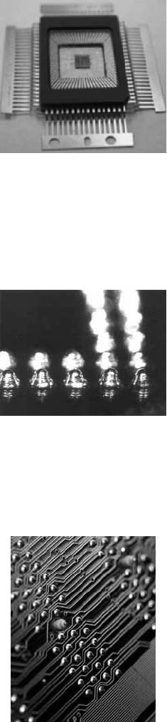
270 CHAPTER SIX implementation fabrics
with different physical, electrical and thermal properties. The choice of
package depends on the number of connections required and the environ-
ment in which the product is to operate, among other factors.
Within a package, the IC is affixed to the bottom of a cavity. Fine gold
wires are connected from pads on the edge of the IC to points on the pack-
age’s lead frame (see Figure 6.17), which is the metal framework leading
to the external package pins. The cavity is then sealed to protect the IC
and the wires. As IC technology has developed, the maximum number of
pins has increased, as have operating speeds. For a high pin-count, high
performance IC, using bond wires introduces mechanical problems and
delays and degrades signals. Recent packages for these ICs have adopted
flip-chip technology. The connection pads on the IC are covered in con-
ductive material forming bumps (Figure 6.18). The IC is then flipped over
and affixed to the substrate of the package, with the bumps in direct con-
tact with substrate connection points. The connection points lead to the
external pins of the package.
The packaged ICs and other components in a system are assembled
together on a printed circuit board (PCB). This consists of layers of fiber-
glass or other insulating material separating layers of metal wiring. The
metal is deposited in a layer on a fiberglass sheet, and then etched using
a photolithographic process, similar to that used in manufacturing ICs.
Several layers are sandwiched together. Small holes are drilled through the
layers and coated with metal to form connections, called vias, between
the layers. The completed PCB contains all the circuit wiring needed for
the product.
One form of PCB, a through-hole PCB (Figure 6.19), includes addi-
tional metal-coated holes into which IC package pins are inserted. Solder,
a metal alloy with a low melting point, is melted into the holes to form
electrical connections between the pins and the PCB wiring. Products using
this form of manufacture need ICs in insertion-type packages, such as
those shown in Figure 6.20. Dual in-line packages (DIPs) have two rows
of pins with 0.1-inch spacing. These were among the first IC packages
to be introduced, being used for SSI and MSI components, but are less
common now. They are relatively large and are limited in the number of
pins they can provide, with a 48-pin DIP being about the largest practical
size. ICs requiring more pins can be packaged in a pin-grid array (PGA)
package, having up to 400 or more pins. However, these have largely
been replaced by newer forms of package, and are now mainly used for
ICs such as computer CPUs that are to be mounted in sockets so that they
can be removed. One of the advantages of through-hole PCBs is that they
can be manually assembled, since the component sizes are manageable.
This is good for low-volume products, since the cost of setting up a
manufacturing run is less than that for automated assembly. However, the
move to ICs with higher pin counts has reduced the applicability of this
technology.
FIGURE 6.17 An IC in a
package with bond-wires connect-
ing to the lead frame.
FIGURE 6.18 Connection
bumps on a fl ip-chip IC.
FIGURE 6.19 A through-
hole PCB.
The second form of PCB is a surface-mount PCB (Figure 6.21),
so-called because components are mounted on the surface rather than
being inserted in holes. This has the advantage of reduced manufactur-
ing cost (for higher-volume products), finer feature sizes and increased
circuit density. Surface mounting IC packages have pins or connection
points that come into contact with a metal pad on the PCB. Solder paste
is applied between each pin and pad and subsequently melted, forming
the connection. There are numerous different surface mounting packages,
some of which are shown in Figure 6.22. Quad flat-pack (QFP) packages
have pins along all four sides, and are suitable for ICs with up to 200 or
so pins. The spacing between pins varies from 1 mm for the packages with
fewer pins, down to 0.65mm for the higher pin-count packages. Fine-
pitch QFP packages allow increased pin count, up to nearly 400 pins, by
reducing the pin spacing to 0.4mm. Given the delicacy of these pins, the
packages are not suitable for manual handling and assembly. The most
common package in use now for high pin-count ICs is the ball-grid array
(BGA) package. Depending on the package size and the pin spacing, BGA
FIGURE 6.20 Insertion-type
IC packages: DIPs (left) and PGAs
(right).
FIGURE 6.21 A surface-
mount PCB.
FIGURE 6.22 Surface
mounting IC packages: QFPs (left)
and BGA (right).
6.3 Packaging and Circuit Boards
CHAPTER SIX 271
272 CHAPTER SIX implementation fabrics
packages can accommodate ICs with up to 1800 pins. Higher pin-count
BGA packages are also being developed.
In recent times, high-density packaging techniques have been developed
for use in products where space is constrained. A good example is a cell
phone, in which small size and reduced weight are important marketing
factors. Rather than placing each IC in a separate package and assem-
bling several packages onto a PCB, multichip modules (MCMs) attach
the bare chips to a ceramic substrate (see Figure 6.23). Interconnection
wires and passive components (resistors and capacitors) are also printed
or soldered onto the substrate. The complete module is then encapsulated
with external connections made through package pins to a PCB. Even
denser packaging can be achieved by building in three dimensions, rather
than laying them out on a two-dimensional surface. For example, chip
stacking involves placing two or more chips in a vertical stack. Connec-
tions can be made between adjacent chips by metal contacts, and between
chips and the containing package by bond wires. Several flash memory
manufacturers are using these techniques to provide high-capacity storage
in very small packages. As demand for high-performance mobile devices
increases, we can expect to see continued development of these high-
density packaging techniques.
1. How does fl ip-chip IC packaging differ from previous packaging
technologies?
2. What distinguishes surface-mount IC packages from insertion-type
packages?
3. What is a via in a PCB?
4. For an IC with 1200 pins, what kind of package would most likely
be used?
6.4 INTERCONNECTION AND SIGNAL
INTEGRITY
When we introduced the digital abstraction in Chapter 1, we described
signals as changing between low and high logic levels instantaneously. We
emphasized, however, that this is an abstraction, and that real signals take
time to change and time to propagate along signal wires. We have taken
a relatively simple view of signal propagation between a source and a
destination within a circuit. In practice, there are a number of complicat-
ing factors, particularly when the source and destination are in different
ICs on a PCB. A signal change must propagate from the source driver,
through the bond wire, package lead frame and pin of the source IC,
along the PCB trace, through the pin, lead frame and bond wire of the
destination IC, and into the receiver. Along this path, there are several
KNOWLEDGE
TEST QUIZ
KNOWLEDGE
TEST QUIZ
FIGURE 6.23 A multichip
module.
influences that can cause distortion of the signal and introduce noise.
The term signal integrity refers to the degree to which these effects are
minimized. If we are using off-the-shelf ICs or PLDs, we do not have
control over the path within the IC package. We must assume that the
designers of the IC and package have done due diligence to maintain sig-
nal integrity. Alternatively, if we are implementing a design in an ASIC,
we must take responsibility for signal integrity within the ASIC. Since this
is a complex area, we largely defer it to an advanced reference on VLSI
design, though many of the ideas that we discuss in this section do apply
to ASIC design. In either case, using off-the-shelf parts or ASICs, we need
to consider the effects of the PCB on signal integrity.
A change in a signal value causes a change in the current flowing
through the PCB trace. This causes a change in the electric and magnetic
fields around the trace. Propagation of those fields determines the speed of
propagation of the signal change along the trace. In common PCB materi-
als, the maximum propagation speed is approximately half the speed of
light in a vacuum. Since the latter is 3 10
8
ms
1
, we can use 150mm
per nanosecond as a good rule of thumb for signal propagation along a
PCB trace. For low speed designs and small PCBs, this element of total
path delay is insignificant. However, for high-speed designs, particularly
for signals on critical timing paths, it is significant. Two cases in point are
the routing of clock signals and parallel bus signals. If a clock signal is
routed through paths of different lengths to different ICs, we may intro-
duce clock skew, in much the same way that we described in Section 4.4.
Similarly, if different signals within a parallel bus are routed along paths
of different lengths, changes in elements of the bus may not arrive con-
currently, and may be incorrectly sampled at the destination’s receiver. In
these cases, it may be necessary to tune the timing of the system by adding
to the length of some PCB traces to match propagation delays. CAD tools
used for PCB layout offer features to help designers perform such tuning
semiautomatically.
A major signal integrity issue in PCB design is ground bounce, which
arises when one or more output drivers switch logic levels. During switch-
ing, both of the transistors in the driver’s output stage are momentarily
on, and transient current flows from the power supply to ground. Ideally,
the power supply can source the transient current without distortion. In
reality, however, there is inductance in both the power and the ground
connections, as shown in Figure 6.24. The inductance causes voltage
spikes in the power supply and ground on the IC. This can cause voltage
spikes on other output drivers, possibly causing false transitions in the
receivers to which they are connected. It can also cause transient shifting
of the threshold voltage of receivers on the IC, causing false transitions
at those receivers. The effect is particularly pronounced when multiple
drivers switch concurrently, for example, when the value on a parallel bus
changes, since the transient current is much greater.
6.4 Interconnection and Signal Integrity CHAPTER SIX 273
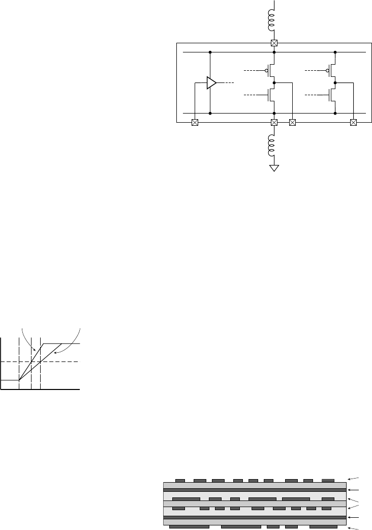
274 CHAPTER SIX implementation fabrics
In order to reduce the effects of ground bounce, we can take a number
of important measures. First, we can place bypass capacitors between
power and ground at strategic places around a PCB. These capacitors
hold a reserve of charge that can quickly supply the needs of switching
drivers. A common rule of thumb is to place a capacitor close to each
IC package. Values of 0.01µF to 0.1µF are common. Second, we can use
separate PCB layers for the ground and power supply (Figure 6.26). This
gives a low-inductance path for the power supply current and its ground
return. It also has other benefits, mentioned below. Third, we can limit
the rate of voltage change (the slew rate) and limit the drive current of
the output drivers. These actions limit the rate of change of current, and
so limit the inductive effect of the change. Components such as modern
FPGAs have programmable output drivers that allow selection of slew
rate and drive current limits. Of course, reducing the slew rate means
that a signal takes longer to change from one logic level to the other, as
illustrated in Figure 6.25. Hence, limiting slew rate may increase propa-
gation delay through circuits, consequently requiring a reduction in clock
rate. This is a case where a trade-off between speed of operation and
noise immunity may be required. Finally, we can use differential signaling,
discussed in Section 6.4.1, as a means of making the system more immune
to noise induced by ground bounce.
IC within package
Bond-wire, lead and
PCB inductance
Bond-wire, lead and
PCB inductance
+V
FIGURE 6.24 Inductance in
the bond-wires, package leads and
PCB connections for power and
ground.
slew-rate
limited
V
th
high
slew rate
FIGURE 6.25 The effect
of slew-rate limiting a signal. The
signal takes longer to reach the
threshold voltage V
th
.
power plane
signal layer
si
g
nal la
y
er
signal layers
ground plane
FIGURE 6.26 Cross section
of a multilayer PCB with ground
and power planes.
Another signal integrity issue for high-slew rate signals is noise due
to transmission-line effects. When the time for a transition between logic
levels is similar to or shorter than the propagation delay along a signal
path, the transition is affected by reflections at the driving and receiving
ends of the path. A full analysis of the effects requires knowledge of the
characteristic impedance of the path, as well as the source impedance of
the driver and the terminating impedance of the receiver. Depending on
the relationships between these values, the signal may suffer from partial
transitions, overshoot, undershoot and ringing (Figure 6.27). The situ-
ation is made more complex if the signal wire is not a simple driver-to-
receiver connection, but has multiple receivers along the path. PCB layout
artifacts, such as vias and branching paths, also introduce further effects.
The main design techniques for managing transmission-line effects
involve appropriate layout and proper termination of PCB traces. By run-
ning a trace of specific dimensions at a controlled distance between two
ground or power planes in the PCB, we create a stripline transmission line
with a controlled characteristic impedance. Where the transmission line
effects are less critical, we can run a trace over just one plane, creating
a microstrip transmission line. For critical signals, we can adopt circuit
designs and layouts that avoid placing receivers along the PCB trace, or
that group them together at the receiving end. Finally, we can include ter-
mination resistors to ensure proper matching of drivers and receivers to
the characteristic impedance of the transmission line. In high-performance
modern components, including FPGAs, the drivers include termination
resistors on the IC. In other cases, we may need to include resistors as
discrete components adjacent to IC pins.
As we mentioned earlier, transitions between logic levels on a signal
cause electromagnetic fields to propagate around the PCB trace. Some of
the field energy is radiated out from the system, and may impinge on other
electronic systems, where it induces noise. This form of unwanted coupling
is called electromagnetic interference (EMI). There are government and
0.5V
0.0V
1.0V
1.5V
2.0V
2.5V
V
IL
V
OL
V
IH
V
OH
overshoot
undershoot
ringing
ringing
FIGURE 6.27 Overshoot,
undershoot and ringing
transmission-line effects.
6.4 Interconnection and Signal Integrity CHAPTER SIX 275
276 CHAPTER SIX implementation fabrics
other regulations that limit the amount of EMI that a system may emit in
various environments, since excessive EMI can be annoying (for example,
if it interferes with your TV reception) or a safety hazard (for example,
if it interferes with your aircraft navigation). Electromagnetic fields from
an “aggressor” PCB trace can also impinge on adjacent traces, inducing
crosstalk on the “victim” traces. The closer the traces and the longer their
parallel paths, the more pronounced the crosstalk effect. As with other
signal integrity issues, appropriate PCB design techniques, such as routing
traces close to ground or power planes, can reduce EMI and crosstalk by
containing the electromagnetic fields. Limiting slew rates of transitions
also reduces the radiated energy, and so reduces EMI and crosstalk.
6.4.1 DIFFERENTIAL SIGNALING
The techniques for maintaining signal integrity that we have discussed so
far are based on reducing the amount of interference induced on signal
wires. Another technique, use of differential signaling, is based on the idea
of reducing a system’s susceptibility to interference. Rather than transmit-
ting a bit of information as a single signal S, we transmit both the positive
signal S_P and its negation S_N. At the receiving end, we sense the voltage
difference between the two signals. If S_P S_N is a positive voltage, then
S is received as the value 1; if S_P S_N is a negative voltage, then S is
received as 0. This arrangement is illustrated in Figure 6.28. The assump-
tion behind the differential signaling approach is that noise is induced
equally on the wires for both S_P and S_N. Such common-mode noise is
cancelled out when we sense the voltage difference. To show this, suppose
a noise voltage V
N
is induced equally on the two wires. At the receiver,
we sense the voltage
(S_P V
N
) (S_N V
N
) S_P V
N
S_N V
N
S_P S_N
For the assumption of common-mode noise induction to hold, differential
signals must be routed along parallel paths on a PCB. While this might
suggest a problem with crosstalk between the two traces, the fact that the
signals are inverses of each other means that they both change at the same
time, and crosstalk effects cancel out.
As well as rejecting common-mode noise, differential signaling also
has the advantage that reduced voltage swings are needed for a given
noise margin. Even though each of S_P and S_N switches between V
OL
and V
OH
, the differential swing at the receiver is between V
OL
V
OH
and V
OH
V
OL
, that is, twice the swing of each individual signal. Reduc-
ing the voltage swing has multiple follow-on effects, including reduced
switching current, reduced ground bounce, reduced EMI, and reduced
crosstalk with other signals. Thus, use of differential signals can be very
beneficial in high-speed designs.
S
S_P
S_N
FIGURE 6.28 A differential
driver and receiver.
1. What is meant by the term signal integrity?
2. How fast does a signal change propagate along a typical PCB trace?
3. What causes ground bounce in digital systems?
4. Where should bypass capacitors be placed on a PCB?
5. How does limiting the slew rate of an output driver improve signal
integrity?
6. What design techniques can be used to mitigate transmission-line
effects, such as overshoot, undershoot and ringing?
7. What are EMI and crosstalk?
8. How does differential signaling improve noise immunity?
9. For a 2.5V low-voltage differential signaling (LVDS) output,
the nominal V
OL
and V
OH
voltages are 1.075V and 1.425V,
respectively. What differential voltage swing is seen at the receiver?
KNOWLEDGE
TEST QUIZ
KNOWLEDGE
TEST QUIZ
6.4 Interconnection and Signal Integrity CHAPTER SIX 277

278 CHAPTER SIX implementation fabrics
6.5 CHAPTER SUMMARY
Improvements in IC manufacturing processes, especially in photo-
lithography, have led to increased circuit speed and density. These
trends are continuing.
Yield, the proportion of manufactured ICs that work, is a significant
determinant of cost. Reducing IC area reduces the chance of a defect
on the IC.
The 74xx00 families of small-scale integrated (SSI) and medium-
scale integrated (MSI) circuits were the main components used in
early and legacy digital systems. There are several 74xx00 families,
varying in speed, power and logic thresholds. For new designs,
74xx00 components are largely superseded by programmable logic
devices.
Application-specific integrated circuits (ASICs) are ICs designed
for particular applications. Application-specific standard products
(ASSPs) are ASICs designed for particular market segments. In both
cases, high non-recurring engineering (NRE) cost limits their use to
high-volume applications, or applications that demand very high
performance.
In a full-custom ASIC, the IC circuitry is custom designed in detail.
In a standard-cell ASIC, the circuit is implemented by a synthesis
tool using predesigned gate and flip-flop cells from a library, thus
reducing NRE cost.
Programmable logic devices (PLDs) are standard parts that are
programmed after manufacture to implement a circuit function.
Programmable array logic (PAL) components are simple PLDs that
implement simple combinational or sequential functions. Generic
array logic (GAL) components include programmable macrocells
instead of fixed-function output logic.
Complex PLDs consist of a number of PAL structures and an inter-
connection network integrated onto a single IC. They are useful for
larger combinational or sequential designs.
Field-programmable gate arrays (FPGAs) consist of an array of
logic blocks, memory blocks and I/O blocks, and a programmable
interconnection network. The logic blocks implement simple com-
binational and sequential functions. Platform FPGAs also incorpo-
rate processor cores, arithmetic circuits and other complex function
blocks.
왘
왘
왘
왘
왘
왘
왘
왘
왘

6.6 Further Reading CHAPTER SIX 279
ICs are embedded in packages and assembled onto printed circuit
boards (PCBs) to form a complete digital system. Different package
types are used for through-hole and surface-mount PCBs.
Signal integrity refers to the minimization of distortion of digital
signals due to parasitic capacitance and inductance. Effects
include signal skew, ground bounce, transmission line effects
(overshoot, undershoot and ringing), electromagnetic interference
(EMI), and crosstalk. Effects are mitigated by careful PCB design.
Differential signaling involves transmitting both a positive signal and
its negation, and sensing the voltage difference between the two at a
receiver. Differential signaling allows common-mode noise rejection
and improved signal integrity.
6.6 FURTHER READING
Exponential Trends in the Integrated Circuit Industry, Scotten W. Jones,
IC Knowledge LLC, 2004, http://www.icknowledge.com/trends/
Exponential2.pdf. A good summary of the way in which a number
of parameter values have changed exponentially over time, and the
interrelationship among the parameters.
Introduction to Integrated Circuit Technology, 3rd Edition, Scotten
W. Jones, IC Knowledge LLC, 2004, http://www.icknowledge
.com/misc_technology/IntroToICTechRev3.pdf. Outlines the steps
involved in manufacture, packaging and test of integrated circuits.
Digital Logic Pocket Data Book, Texas Instruments, Inc., 2002,
http://focus.ti.com/lit/ug/scyd013/scyd013.pdf. Contains datasheets
for 74xx00 family SSI, MSI and bus transceiver components.
CMOS VLSI Design: A Circuits and Systems Perspective, 3rd Edition,
Neil H. E. Weste and David Harris, Addison-Wesley, 2005. An
advanced reference on CMOS VLSI circuit design.
Signal Integrity Issues and Printed Circuit Board Design, Douglas
Brooks, Prentice Hall, 2003. Introduces basic electrical character-
istics of PCBs and components, and covers propagation delays,
electromagnetic interference, transmission lines, crosstalk and
power-supply decoupling. The author’s website at www.ultracad.com
provides numerous articles on these topics.
High-Speed Digital Design: A Handbook of Black Magic, Howard
Johnson, Prentice Hall PTR, 1993. Covers aspects of analog circuit
behavior that are relevant to high-speed digital circuit design,
including signal integrity issues.
왘
왘
왘

280 CHAPTER SIX implementation fabrics
exercise 6.1 The 74LS85 component is a 4-bit cascadable magnitude
comparator for unsigned binary integers. Details are provided in the Texas
Instruments Digital Logic Pocket Data Book (see Section 6.6, Further Reading).
Design a 16-bit magnitude comparator using four 74LS85 components and any
additional gates required.
exercise 6.2 Suppose a company is deciding between an ASIC and an
FPGA implementation for a complex new design. Their estimates of NRE costs
for the two alternatives are:
EXERCISESEXERCISES
The unit cost for manufacture of each ASIC will be $15.00, and the unit
cost of purchasing and programming each FPGA will be $25.00. Which option is
more cost-effective for production volumes of 100,000 units; 200,000 units; and
500,000 units? What is the production cost at which the two options are equally
cost-effective?
exercise 6.3 On a copy of Figure 6.9, draw the fuses that are required to
implement the following Verilog assignments in a PAL16L8:
a)
assign O8 = I1 ? ~I9 | I10 : 1'bz;
b) assign IO2 = ~(I1 & ~I2) | (~I1 & I3& ~I8);
c) assign IO7 = (I1 & ~I2) | (~I3 & I10);
exercise 6.4 Describe how an OLMC of a GAL22V10, shown in
Figure 6.12, should be programmed to emulate the input/output circuit of:
a) IO2 of a PAL16L8
b) O1 of a PAL16L8
c) I1 of PAL16L8
d) an output of a PAL16R8
nre cost component asic fpga
Staff $2,500,000 $2,000,000
Infrastructure $1,500,000 $1,000,000
Consumables and Services $750,000 $100,000
281
processor basics
In this chapter we start our focus on embedded systems with an introduction
to the kinds of processors that are used. We describe the way processors
operate and give examples of the instructions that make up embedded
software programs. We also describe the way instructions and data are
encoded in binary and stored in memory. Finally, we examine ways of
connecting the processor with memory components.
7.1 EMBEDDED COMPUTER
ORGANIZATION
In Section 1.5.1, we introduced the idea of an embedded system, in which
one or more computers form part of the system. The computers run
programs that implement the functions required of the system. Unlike
a general-purpose PC, a computer in an embedded system has just those
resources required to support its specialized operation. In this section, we
will describe some of the general properties of embedded systems and the
processing elements they contain. We won’t deal with how the processing
elements are designed; that is a significant field of study in its own right.
Instead, we will treat them as black-box circuit components that we can
use to build a digital system.
A computer embedded in a digital system generally contains the
elements shown in Figure 7.1. The central processing unit (CPU), often
called a processor core when it is embedded as part of an IC, is the ele-
ment that processes data according to a program. The kinds of process-
ing it can perform include the arithmetic operations that we described in
Chapter 3. It can also evaluate logical conditions and select among alter-
nate operations based on the outcomes of the conditions. We will describe
the way a program is formed in more detail in Section 7.2. Meanwhile,
suffice it to say that the program is encoded in binary form and stored
in the instruction memory shown in the figure. The data upon which the
program operates are also encoded in binary form and stored in the data
7
282 CHAPTER SEVEN processor basics
memory. In both cases, the memory is implemented using the kinds of
memory components we described in Chapter 5. Whereas general pur-
pose computers, such as PCs, usually store the instructions and data in
the same memory, embedded computers typically separate the two. (This
arrangement is often referred to as a Harvard architecture, named after
the institution where the idea originated. The conventional approach with
a single memory for instructions and data is called a von Neumann archi-
tecture, after the person who first described it.) The reason for the separa-
tion is that the instructions in an embedded computer are usually fixed
during the manufacture of the system (or only occasionally upgraded in
the field), and the amount of instruction memory required is known in
advance. Hence, we usually store instructions in a ROM or flash memory
component, and provide a RAM for the data memory. This differs from a
general-purpose computer, in which one or more different programs need
to be started at different times and run concurrently, and the amount of
instruction memory is not known in advance.
The input, output and input/output (I/O) controllers in Figure 7.1
allow the computer to acquire data to be processed (input) and to deliver
the results (output). In many embedded systems, the input data comes
from sensors that sample physical properties, such as temperature, posi-
tion, time, and so on. Similarly, the output data causes actuators to have
a physical effect, such as moving a lever, turning a motor, heating some
material, and so on. Input and output controllers can also deal with a
user interface, consisting of switches, buttons and knobs for input and
lights and LCD panels for outputs. For a complex user interfaces, devices
such as a keyboard, mouse or display screen, as used in a general purpose
computer, might also be employed. In all cases, the job of the input/output
controller is to transform between a physical property or effect and a cor-
responding binary representation that can be processed by the CPU. We
will describe how this can be done and how the CPU accesses the binary
representation in Chapter 8.
The accelerator in Figure 7.1 is a specialized circuit designed to
implement specific processing operations with higher performance
than can be achieved using the CPU. Not all embedded systems include
CPU
…
Accelerator
Instruction
memory
Input
controller
Output
controller
I/O
controller
Data
memory
FIGURE 7.1 Elements of an
embedded computer.
accelerators. The choice of whether to include an accelerator for any
operation depends on the functional and performance requirements of
the application, together with cost and other constraints that apply. We
will discuss accelerators in more detail in Chapter 9, in which we include
as an extended example an accelerator for detecting edges of objects in
video images.
The final element in Figure 7.1 is the interconnection between the
other elements. We use the term bus to refer to the collection of signals
that form the interconnection. The figure shows just one bus connecting
all of the elements. However, in more elaborate systems, there may be sep-
arate buses for connecting the memory and the input/output controllers
with the CPU. There may even be separate buses for the instruction and
data memories, since many high-performance processors can read further
instructions concurrently with access to data by previous instructions.
Accelerators, if included, might be connected to the CPU using the same
bus as the memory, or using a separate dedicated bus. Figure 7.2 shows
one possible organization for a high-performance embedded system with
multiple buses. In this chapter, we will focus on the bus connecting the
CPU and memory, and defer consideration of bus connections to input
and output controllers and to accelerators until later chapters.
7.1.1 MICROCONTROLLERS AND
PROCESSOR CORES
CPUs for embedded systems come in a range of sizes for different applica-
tions. Some are single-chip microprocessors, consisting of a CPU by itself
in a package. Most CPUs used in general-purpose PCs are also available
in versions suitable for embedded applications. Examples include Pentium
family CPUs from Intel and the PowerPC from Freescale Semiconductor.
Other microprocessors are designed specifically for embedded applications.
7.1 Embedded Computer Organization CHAPTER SEVEN 283
CPU
Accelerator
Instruction
memory
Input
controller
Output
controller
I/O
controller
Data
memory
FIGURE 7.2 Organization of
a high-performance embedded
computer with multiple buses:
one for the instruction memory,
one for the data memory and an
accelerator, and one for input/
output controllers.
284 CHAPTER SEVEN processor basics
In both cases, we need to provide memory and I/O controllers as separate
chips on a PCB. In contrast, single-chip microcontrollers include a CPU,
instruction and data memory, and I/O controllers all in the one package.
Many microcontroller vendors provide a family of chips, each with the
same CPU, but varying in the amount of memory and the selection of
I/O controllers. In some microcontroller families, the CPUs are relatively
simple, operating just on 8-bit or 16-bit data, with relatively low per-
formance. Other families have more complex CPUs that can operate on
data up to 32 bits in length. The combination of a CPU with the on-chip
memory and I/O controllers makes them suitable for a large range of cost-
sensitive, low-performance applications.
An alternative to using a fixed function microprocessor or microcon-
troller is to include a CPU in an FPGA component. This has the advantage
that the input/output controllers can be customized for an application,
but still be included in the same package as the CPU. The CPU in the
FPGA can be implemented as a fixed-function block embedded within
the programmable fabric. The Virtex-II Pro and Virtex 4 FPGAs from
Xilinx take this approach, and include one or more PowerPC processor
cores. Alternatively, the CPU can be implemented as a soft core using the
programmable resources of the FPGA. FPGA vendors provide soft core
processor designs that users can include as part of their system. Examples
include the MicroBlaze core from Xilinx, the Nios-II core from Altera,
and the ARM core from Actel. These are all relatively high-performance
CPUs that operate on data up to 32 or 64 bits in length. For simpler
designs, a smaller soft core that operates on 8-bit data may suffice. It
would take up less of the FPGA resources, and would fit in a smaller and
cheaper FPGA component. The Xilinx PicoBlaze soft core is an example,
as is the Gumnut core that we will introduce in Section 7.2.
If our design is implemented in an ASIC, we can also include a CPU
and customized memory and input/output controllers. Several vendors
provide processor core designs that can be included as blocks in ASICs.
Among the most widely used are the ARM cores from ARM Ltd, the
PowerPC cores from IBM, and the MIPS cores from MIPS Technologies.
Given that we can customize the design on an ASIC, there is also oppor-
tunity to customize the CPU itself. Tensilica Inc. is a vendor that provides
a customizable CPU based on the requirements of the program to be exe-
cuted. Their approach involves analyzing the program and including only
the CPU features needed to execute that program. They also allow exten-
sion of the CPU with customized hardware for specialized operations.
A final approach to mention is to include one or more digital signal
processors (DSPs). These are specialized processing elements optimized for
the kinds of operations involved in dealing with digitized signals, such as
audio, video or other streams of data from sensors. Many signal process-
ing applications require fixed-point or floating-point arithmetic operations
to be performed at a high rate on large volumes of data. An ordinary CPU
would not be able to meet the performance requirements. Nonetheless, such
applications often need a conventional CPU to perform other operations,
such as interacting with the user and overall coordination of system opera-
tion. Hence, DSPs are often combined with conventional CPUs in hetero-
geneous multiprocessor systems. Modern cell phones are good examples.
Another approach to providing DSP functionality is to extend a conventional
CPU with additional hardware and instructions for digital signal processing.
Some processor cores from ARM and MIPS include such extensions, and
Tensilica processor cores can be similarly customized. Since digital signal
processing is an advanced topic, we will defer consideration of DSP cores
and embedded multiprocessor systems to advanced reference books.
1. What are the main elements of an embedded computer?
2. Why do embedded computers usually have separate instruction and
data memories?
3. What is the difference between a microprocessor and a micro-
controller?
4. What is meant by a soft core processor in an FPGA?
7.2 INSTRUCTIONS AND DATA
The function performed by a CPU is specified by a program, which
consists of a sequence of instructions. Each instruction specifies one sim-
ple step in the program, such as getting a piece of data from memory, or
adding two numbers. The repertoire of instructions for a given CPU is
called the instruction set of the CPU. We also use the term instruction set
architecture (ISA) to refer to the combination of the instruction set and
other aspects of the CPU that are visible to the programmer. CPUs from
different vendors have quite significantly different instruction sets, so a
sequence of instructions developed for one CPU will not work on a CPU
from a different vendor. When we develop the program for an application,
we usually use a high-level language, such as C, C or Ada, and use a
software tool called a compiler to translate the program into a sequence
of instructions that performs the same operations. Apart from allowing
us to work at a higher level of abstraction, this has the advantage that the
program can be ported to work on a CPU with a different instruction set
simply by using a different translator. However, when we are developing
an embedded system in which the CPU interacts with circuits that we
design, we often need to monitor the instruction-by-instruction operation
of the CPU as we test and debug the design. At this level, it is important to
understand how a CPU represents and processes individual instructions.
We will just describe CPU operation at this level, and defer a discussion of
programming using high-level languages to other books.
KNOWLEDGE
TEST QUIZ
KNOWLEDGE
TEST QUIZ
7.2 Instructions and Data CHAPTER SEVEN 285
286 CHAPTER SEVEN processor basics
The instructions of a program are encoded in binary and stored in
successive locations of the instruction memory. The CPU executes the pro-
gram by repeatedly following these steps:
1. Fetch the next instruction from the instruction memory.
2. Decode the instruction to determine the operation to perform.
3. Execute the operation.
In order to keep track of which instruction to fetch next, the CPU has
a special register called the program counter (PC), in which the address of
the next instruction is kept. In the fetch step, the CPU uses the contents of
the PC to do a read access from the instruction memory, and then incre-
ments the PC value. In the decode step, the CPU determines the resources
required to perform the operation specified by the instruction. In a simple
CPU, the decode step is correspondingly simple. In a larger CPU, however,
decoding may involve such actions as checking for resource conflicts and
availability of data, and waiting until resources are free. In the execute
step, the CPU activates the appropriate internal resources to perform the
operation. This involves setting control signals to make multiplexers sup-
ply the required operands and arithmetic hardware perform the required
operation, and enabling registers to receive results. In a simple CPU, these
steps are performed in order, and when the execute step is finished, the
CPU starts again with the fetch step. More complex, high performance
CPUs, however, can overlap the steps, provided they produce the same
outcome as if the steps were performed in order. Techniques used within
CPUs to execute several instructions in parallel include pipelining and
superscalar execution, described in the reference book on computer archi-
tecture (see Section 7.5).
The data on which instructions operate is encoded in binary in fixed-
size quantities. The smallest data item is usually 8 bits, called a byte. It
is often used to represent an unsigned or a signed integer, or a character.
Simple CPUs can only operate on 8-bit data, so they are referred to as
8-bit CPUs. Larger CPUs can operate on 16-bit or 32-bit words of data,
as well as on 8-bit data, so they are referred to as 16-bit or 32-bit CPUs,
respectively.
Regardless of the sizes of data that can be operated upon, the data
memory is usually organized with 8-bit locations, each separately
addressed. 16-bit or 32-bit data is stored in two or four successive loca-
tions. The order of the bytes within a word varies between CPUs, as shown
in Figure 7.3. Little-endian CPUs store the byte containing the least signif-
icant bits at the lower address and the byte containing the most significant
bits at the higher address. In contrast, big-endian CPUs store the bytes
in the opposite order. (The terms “little endian” and “big endian” origi-
nated in Jonathan Swift’s Gulliver’s Travels, in which the people of two
countries fight over which end of their breakfast eggs should be cut open.
The terms were adopted by Danny Cohen in an article, cited in Section 7.5,
in which he argues that either byte ordering is acceptable, provided it is
used consistently.) Some CPUs require that 16-bit data be stored at even
addresses and that 32-bit data be stored at addresses that are a multiple of
four. Others allow 16-bit and 32-bit data to be stored at any address.
7.2.1 THE GUMNUT INSTRUCTION SET
Rather than trying to describe the characteristics of the instruction sets
of all CPUs, we will present one relatively simple example that embod-
ies most of the important concepts. The CPU that we will describe is
an 8-bit soft core called the Gumnut, developed by the author. (A gum-
nut is a small seedpod of an Australian eucalyptus tree. It is something
small from which large things grow.) Further information and files are
provided in the supplementary material for this book for use in FPGA
designs. The complete Gumnut instruction set is listed in Table 7.1. We
use a notation for instructions called assembly code. An assembly-code
program can be translated by a software tool called an assembler into a
sequence of binary-coded instructions to be loaded into the instruction
memory.
The Gumnut has an instruction memory of up to 4096 instructions
(using 12-bit addresses) and a data memory of 256 bytes (using 8-bit
addresses). When the CPU is reset, it clears the PC to 0, and starts the
fetch-decode-execute cycle, fetching the first program instruction from
address 0 in the instruction memory. Within the CPU, there are eight
general-purpose registers, named r0 through r7, that can hold data to
be operated upon by instructions. Register r0 is special, in that it is
hard-wired to have the value 0, and any updates to it are ignored. The
CPU also has two single-bit condition-code registers called Z (zero) and
7.2 Instructions and Data CHAPTER SEVEN 287
0
least sig. byte
Little endian
Big endian
8-bit data
16-bit data
32-bit data
most sig. byte
least sig. byte
most sig. byte
m
m + 1
n
n + 2
n + 3
n + 1
0
least sig. byte
8-bit data
16-bit data
32-bit data
most sig. byte
least sig. byte
most sig. byte
m
m + 1
n
n + 2
n + 3
n + 1
FIGURE 7.3 Little-endian
(left) and big-endian (right)
memory layout for data words.

288 CHAPTER SEVEN processor basics
instruction description
Arithmetic and logical instructions
add rd, rs, op2 Add rs and op2, result in rd
addc rd, rs, op2 Add rs and op2 with carry, result in rd
sub rd, rs, op2 Subtract op2 from rs, result in rd
subc rd, rs, op2 Subtract op2 from rs with carry, result in rd
and rd, rs, op2 Logical AND of rs and op2, result in rd
or rd, rs, op2 Logical OR of rs and op2, result in rd
xor rd, rs, op2 Logical XOR of rs and op2, result in rd
mask rd, rs, op2 Logical AND of rs and NOT op2, result in rd
Shift instructions
shl rd
,
rs, count Shift rs value left count places, result in rd
shr rd, rs, count Shift rs value right count places, result in rd
rol rd, rs, count Rotate rs value left count places, result in rd
ror rd, rs, count Rotate rs value right count places, result in rd
Memory and I/O instructions
ldm rd, (rs) ± offset Load to rd from memory
stm rd, (rs) ± offset Store to memory from rd
inp rd, (rs) ± offset Input to rd from input controller register
out rd, (rs) ± offset Output to output controller register from rd
Branch instructions
bz ± disp Branch if Z is set
bnz ± disp Branch is Z is not set
bc ± disp Branch if C is set
bnc ± disp Branch if C is not set
Jump instructions
jmp addr Jump to addr
jsb
addr Jump to subroutine at
addr
Mi
scellaneous instructions
ret Return from subroutine
reti Return from interrupt
enai Enable interrupts
disi Disable interrupts
wait Wait for interrupts
stby Enter low-power standby mode
TABLE 7.1 The Gumnut
instruction set. rd and rs are regis-
ters, op2 is a register (rs2) or an
immediate value (immed), count is
count of number of places to shift
or rotate, disp is a displacement
from the next-instruction address,
and addr is a jump target address.

C (carry). They are set to 1 or cleared to 0 depending on the result of
certain instructions, and can be tested to decide among alternative courses
of action in the program.
Arithmetic and Logical Instructions
The arithmetic and logical instructions operate on 8-bit data values
stored in the CPU’s general-purpose registers and store the result in
the destination register, rd. For each instruction, one value is taken
from a source register, rs. The other value, op2, either comes from
a second source register (rs2) or is an immediate value (immed). An
immediate value is a value that is specified as part of the instruction,
rather than being stored in a register or in memory. For example, the
instruction
add r3, r4, r1
adds the values currently in registers r4 and r1 and puts the result in r3.
Similarly, the instruction
add r5, r1, 2
adds the immediate value 2 and the value currently in r1 and puts the
result in r5. Note that the destination register can be the same as a source
register. For example, the instruction
sub r4, r4, 1
updates register r4 by decrementing its value.
The addition and subtraction instructions treat the data values as
8-bit unsigned integers. The addc instruction includes the value of the
C condition code as a carry-in bit, and the subc instruction includes
the C value as a borrow-in bit. All of the instructions in this group modify
the Z and the C bits. They set Z to 1 if the instruction result is 0, and they
clear Z to 0 if the result is nonzero. The add and addc instructions set C
to the carry-out bit of the addition, the sub and subc instruction set C to
the borrow out of the subtraction, and the remaining logical instructions
clear C to 0. We will see later in this section how the condition-code bits
are used by branch instructions.
7.2 Instructions and Data CHAPTER SEVEN 289

290 CHAPTER SEVEN processor basics
example 7.1 Write a sequence of instructions to evaluate the expression
2x 1, assuming the value of x is in register r3 and the result is to be put in r4.
solution We can multiply x by 2 by adding it to itself. The required
instructions are
add r4, r3, r3
add r4, r4, 1
example 7.2 Write a sequence of instructions that sets the Z bit to 1 if
the least significant 4 bits of r2 have the value 0101.
solution We can test whether a register value is equal to 0101 by
subtracting 0101 from the value and putting the result in r0. The result value
is ignored, but Z is set as a side-effect of the subtraction. However, the most
significant 4 bits of r2 might contain 1s that we are not interested in, so we need
to clear them to 0s before doing the subtraction. We can use an AND operation
with the value 00001111 to clear the bit. The required instructions are:
and r1, r2, 0x0F
sub r0, r1, 0x05
The notation “0x” is a prefix for a hexadecimal value in the Gumnut assembly
code notation. Thus, 0x0F is the value 00001111 and 0x05 is the value
00000101.
Shift Instructions
The shift instructions shift or rotate 8-bit values taken from the general
purpose register rs and store the result in register rd. The number of places
to shift or rotate is specified in the instruction as count. For example, the
instruction
shl r4, r1, 3
reads the value currently in register r1, shifts it left by 3 places and puts the
result in r4. The shift-left and shift-right instructions discard the bits shifted
past the end of the 8-bit byte and fill the vacated bit positions with 0s. The
rotate-left and rotate-right instructions copy the bits shifted past the end of
the byte around to the other end. All of these instructions set Z to 1 if the

instruction result is 0, and they clear Z to 0 if the result is nonzero. They set
the C bit to the value of the last bit shifted past the end of the byte.
example 7.3 Write instructions that multiply the value in r4 by 8,
ignoring the possibility of overfl ow.
solution Recall from Section 3.1.2 that we can multiply an unsigned
binary integer by 2
k
by shifting k places to the left. Thus, since 8 2
3
, an
instruction to multiply r4 by 8 is
shl r4, r4, 3
Memory and Input/Output Instructions
The Gumnut has separate instructions for accessing data memory and I/O
controllers. We will discuss the operation of I/O controllers in detail in
Chapter 8. For now, we simply point out that I/O controllers have regis-
ters that govern their operation, and that these registers can be read and
written by the CPU. Just as locations in memory have addresses, each
I/O controller register has an identifying address. The Gumnut uses 8-bit
addresses for I/O controller registers, distinct from the 8-bit addresses it
uses for locations in the data memory. We say that the Gumnut has separate
address spaces for data memory and for I/O controller registers. This is in
contrast to a number of other CPU instructions sets, in which I/O control-
ler registers are part of the same address space as memory addresses. In
those instruction sets, we say I/O registers are memory mapped.
For all of the Gumnut’s memory and I/O instructions, the address to
access is computed by adding the current value in rs and an offset value
specified in the instruction. The load from memory instruction reads from
the data memory at the computed address and puts the read value in reg-
ister rd. The store to memory writes the value from register rd to the data
memory at the computed address. The input and output instructions per-
form similar operations, but read or write to the I/O controller registers at
the computed address. None of these instructions affect the values of the
Z and C bits. As examples, the instruction
ldm r1, (r2)+5
calculates the memory address by adding the current value of r2 and the
offset 5. It then reads from memory at that address and puts the read
value in r1. Similarly, the instruction
7.2 Instructions and Data CHAPTER SEVEN 291

292 CHAPTER SEVEN processor basics
stm r1, (r4)–2
stores the value from r1 into memory at the address 2 less than the current
value of r4.
If we want to specify a particular address to access, we can use r0 as
the register for rs. Recall that r0 always contains 0, so adding it to the
offset value specified in the instruction just gives the offset value. In this
case, we usually interpret the offset value as an unsigned 8-bit address.
Our assembler tool allows us to imply the specification “(r0)” by omis-
sion and just write the address value, for example,
inp r3, 156
which reads from the I/O controller register at address 156 into r3. Simi-
larly, if a register contains the address we want to access, we can use an
offset of 0. Again, our assembler allows us to imply a 0 offset by omission,
as in the instruction.
out r3, (r7)
example 7.4 Write instructions that increment a 16-bit unsigned integer
stored in memory. The address of the least signifi cant byte is in r2. The most
signifi cant byte is in the next memory location.
solution Since the Gumnut arithmetic instructions only operate on 8-bit
data, we need to do two adds, with the carry from the first used in the second.
The instructions are
ldm r1, (r2)
add r1, r1, 1
stm r1, (r2)
ldm r1, (r2)+1
addc r1, r1, 0
stm r1, (r2)+1
Since the load and store instructions do not affect the C bit, the C result from
the first addition is preserved and used in the
addc instruction.

Branch Instructions
The branch instructions allow us to conditionally change the normal flow of
execution. We mentioned earlier that the CPU follows a fetch-decode-execute
loop to execute instructions at successive addresses in the instruction memory.
It uses a program counter (PC) register to keep track of the next instruc-
tion address, and increments this register after fetching each instruction. The
branch instructions modify the sequential flow of execution by changing the
PC value. Each form of branch tests a condition, and if the condition is true,
adds a signed 8-bit displacement value to the PC. The displacement, specified
in the instruction, indicates how many locations forward or backward the
next instruction to execute is from the current instruction. (A displacement
of 0 refers to the instruction after the branch, since the PC has already been
incremented after fetching the branch instruction.) If the condition is false, the
PC is unchanged, and execution continues sequentially. The different branch
instructions allow us to test each of the Z and C condition code bits for being
set to 1 or not set to 1. Since these bits are affected by arithmetic, logical and
shift instructions, we often deliberately precede a branch instruction with one
of these instructions to compare data values. In other cases, the condition
code setting occurs as a serendipitous side effect of data operations that we
need to perform anyway.
example 7.5 Suppose the value in data memory location 100 represents
the number of seconds elapsed in a time interval. Write instructions to increment
the value, wrapping around to 0 when the value increments above 59.
solution One possible sequence of instructions is
ldm r1, 100
add r1, r1, 1
sub r0, r1, 60
bnz +1
add r1, r0, 0
stm r1, 100
The first two instructions load the value into r1 and increment it. The sub
instruction subtracts 60 from the new value and discards the result (by
using r0 as the destination register). However, the Z condition code is
updated as a side effect. If the new value is 60, the subtraction result is 0,
so Z is set to 1; otherwise, it is cleared to 0. The branch instruction skips
forward one instruction if Z is 0. The intervening
add instruction, which is
only executed when the incremented value was 60, overwrites the incremented
value with 0. The final instruction, executed in all cases, stores the final value
back to memory.
7.2 Instructions and Data CHAPTER SEVEN 293
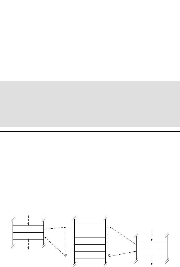
294 CHAPTER SEVEN processor basics
Jump and Miscellaneous Instructions
The first of the jump instructions, jmp, unconditionally breaks the sequen-
tial flow of execution by setting the PC to the address specified in the
instruction.
example 7.6 Write instructions that test whether r1 is 0, and if so, clear
the contents of memory location 100. If r1 is other than 0, the instructions
should clear the contents of memory location 200 instead. Assume that the
instructions start at address 10 in the instruction memory.
solution In the required sequence of instructions we have two alternative
actions to perform, depending on whether r1 is 0. Since instructions are laid out
in linear order in the instruction memory, we need to put the instructions for the
two alternatives one after the other. We need an unconditional jump at the end
of the first alternative to bypass the instructions for the second alternative. The
instructions are
10: sub r0, r1, 0
11: bnz +2
12: stm r0, 100
13: jmp 15
14: stm r0, 200
15: ...
The second of the jump instructions, jsb, is somewhat more involved
than the simple jump instruction. It allows us to execute a subroutine,
that is, a collection of instructions that perform some desired operations
and that we can invoke from different parts of the program. Start-
ing execution of a subroutine is referred to as calling the subroutine.
The jsb instruction is used in tandem with the ret instruction, which
returns from the subroutine to the place of the call. The sequence of
instruction execution for a subroutine is shown in Figure 7.4. Execu-
tion proceeds sequentially until the jsb is encountered. The jsb saves
subroutine
instructions
…
…
…
ret
m
jsb m
…
jsb m
FIGURE 7.4 Flow of execu-
tion of subroutine calls. The
subroutine is called from different
places in the program, and in each
case, returns to the instruction
following the jsb.

7.2 Instructions and Data CHAPTER SEVEN 295
the incremented PC value (the return address) in an internal register
and then updates the PC with the subroutine address specified in the
instruction. This causes instructions in the subroutine to be executed.
Eventually, the subroutine executes a
ret instruction, which restores
the saved return address to the PC. Thus, execution continues with the
instruction after the jsb. The program can include several jsb instruc-
tions that all refer to the same subroutine. In each case, the return
address saved is the address of the instruction after the jsb. This allows
execution to return to the right place, regardless of where the subrou-
tine was called from.
The instructions in the subroutine can include any in the CPU’s
instruction set. This raises the possibility that the subroutine might
include a jsb to call a sub-subroutine. The sub-subroutine might include
a further jsb to call a sub-sub-subroutine, and so on. When the sub-
sub-subroutine returns, execution should continue just after the jsb in
the sub-subroutine, and when it returns, execution should continue just
after the jsb in the subroutine. In order to achieve this effect, the CPU
needs more than just a single register to save return addresses. In fact,
it needs a push-down stack of registers, as shown in Figure 7.5. Each
time a jsb is executed, the return address for that jsb is pushed onto the
stack. When a ret is executed, the return address used is the top entry
on the stack, and that entry is popped from the stack. The Gumnut has
a return-address stack that can hold up to eight entries, which is ample
for most programs.
example 7.7 Suppose an application keeps track of a number of time
intervals concurrently. Revise the sequence of instructions from Example 7.5 to
form a subroutine that increments the number of seconds stored in the memory
location whose address is in r2. Show how to call the subroutine to increment
values in locations 100 and 102.
solution We can rewrite the instructions to form a subroutine as
follows:
ldm r1, (r2)
add r1, r1, 1
sub r0, r1, 60
bnz +1
add r1, r0, 0
stm r1, (r2)
ret
Assuming the first instruction in the subroutine is at location 20 in the instruction
memory, the calling instructions are
return addr for first call
return addr for second call
return addr for first call
return addr for second call
return addr for third call
FIGURE 7.5 The push-down
return-address stack after two
nested calls (top) and a third
nested call (bottom).

296 CHAPTER SEVEN processor basics
add r2, r0, 100
jsb 20
add r2, r0, 102
jsb 20
The remaining miscellaneous instructions deal with interrupts, which
are a way of responding to events signaled by I/O controllers. The enable-
interrupt instruction allows the CPU to respond to interrupt events, and
the disable-interrupt instruction prevents the CPU from responding.
When the CPU responds to an interrupt event, it saves the address of the
instruction it is about to execute and, instead, starts executing instruc-
tions in a special subroutine called an interrupt handler. The interrupt
handler finishes with a return-from-interrupt (reti) instruction rather than
a ret instruction. The wait instruction suspends execution until an inter-
rupt occurs, and the stby instruction enters a low-power standby mode
until an interrupt occurs. The difference is that the CPU would normally
be able to respond to an interrupt immediately when suspended using a
wait instruction, whereas it could take some time to power up from a stby
instruction. We will describe interrupt processing in more detail as part of
our discussion of input/output in Chapter 8.
7.2.2 THE GUMNUT ASSEMBLER
As we mentioned earlier, programs can be written in assembly language and
translated into a sequence of binary-coded instructions by an assembler.
The supplementary material for this book includes a simple assembler
for the Gumnut, called gasm. The gas User Guide, also included in the
supplementary material, provides a detailed description of the assembly
language and how to use the assembler. We will describe a few key points
here, illustrated by the program in Figure 7.6.
; Program to determine greater of value_1 and value_2
text
org 0x000 ; start here on reset
jmp main
; Data memory layout
data
value_1: byte 10
value_2: byte 20
result: bss 1
(continued)
FIGURE 7.6 A Gumnut
assembly language program to
fi nd the greater of two values.

; Main program
text
org 0x010
main: ldm r1, value_1 ; load values
ldm r2, value_2
sub r0, r1, r2 ; compare values
bc value_2_greater
stm r1, result ; value_1 is greater
jmp finish
value_2_greater: stm r2, result ; value_2 is greater
finish: jmp finish ; idle loop
We have seen in Verilog models that we can include comments,
starting with the characters “//”, to describe parts of the model. We can
also include comments in assembly language programs. In Figure 7.6,
comments start with the “;” character and extend to the end of the line.
Comments are especially important in assembly language programs, since
each instruction performs only a single simple step. We use comments to
describe the larger intent of a sequence of instructions.
The assembler lets us specify both the instructions to be included in
the instruction memory and the contents of the data memory. We tell the
assembler which memory we are specifying using the text (for instruction
memory) and data (for data memory) directives. A directive does not rep-
resent a CPU instruction. Rather, it tells the assembler what to do when
translating the program. Rather than requiring us to specify the address
for each instruction and data item, the assembler adds instructions and
data items at increasing addresses in each memory, starting at address 0. It
automatically keeps track of where it is up to by using a location counter
for each of the instruction and data memories. We can direct the assem-
bler to change the location counter for the memory currently being filled
by using an org (short for “origin”) directive. For example, in Figure 7.6,
the org 0x010 directive in the second text segment tells the assembler to
continue placing instructions from location 010
16
.
Within a data segment, we can include directives that specify the
initial contents of data memory locations. The byte directive speci-
fies the contents of an 8-bit location. The bss (short for “block starting
with symbol”) directive reserves a specified number of bytes of memory
storage without initializing their content. We can precede each of these
directives with a label that represents the starting address of the loca-
tions. The assembler works out the address for us. We can then refer to
the label in instructions in the program. For example, the ldm instruc-
tions in Figure 7.6 refer to the labels value_1 and value_2 to load the
initialized content of the data memory locations, and the stm instruction
refers to the label result to store the greater value in the reserved location.
7.2 Instructions and Data CHAPTER SEVEN 297
FIGURE 7.6 (continued)
A Gumnut assembly language
program to fi nd the greater of two
values.
298 CHAPTER SEVEN processor basics
The advantage of using labels is that, when we revise the program, we
don’t need to revise the address values, since the assembler will work out
new values when the program is reassembled.
Within a text segment, we include the instructions that form the
program. Each instruction can be labeled, and the labels can be refer-
enced in branch and jump instructions. Again, the assembler works out
the instruction addresses represented by the labels, so that we don’t have
to work out branch displacements manually, or update references when
we change the program.
One final point to note about the program in Figure 7.6 is that, once it
completes its task, it doesn’t stop executing. The Gumnut does not include
any instructions for stopping. Instead, we include a busy loop at the end
of the program. This just consists of an instruction that jumps back to
itself, performing no useful work. Busy loops are common in embedded
systems, since we usually do not want an embedded computer to stop
(unless we turn the power off). An alternative is to have a CPU instruc-
tion or other facility that suspends operation until some activity is needed,
such as responding to an I/O event. (On the Gumnut, we could use a wait
or stby instruction.) This has the advantage that power consumption in
the suspended state is typically much lower than in the active state. For
this reason, suspending is preferred in battery-powered and other power-
sensitive applications.
7.2.3 INSTRUCTION ENCODING
The instructions of a program are a form of information, and so, like
any other information, can be encoded in binary. If we were to list all
of the possible instructions, taking into account the operation to be per-
formed and any registers, addresses, immediate values, and so on, we
could devise an instruction coding taking up the smallest number of bits.
However, decoding instructions would then be complex, leading to a large
and slow decoder circuit within the CPU. Instead, instruction sets are usu-
ally encoded by separating a code word into distinct fields, each of which
encodes one aspect of an instruction. The primary field is the opcode,
short for operation code, that specifies the operation to be performed and,
by implication, the layout of the remaining fields within the code word.
By keeping the field layout simple and regular, we make the circuit for the
instruction decoder simple and, hence, fast.
As an illustration, the instruction encoding for the Gumnut is shown
in Figure 7.7. (The full details of the instruction encoding are described in
Appendix D.) Each instruction code word is 18 bits long. The left-most
bits, together with the function code (fn), form the opcode. Those instruc-
tions that specify register numbers have the numbers encoded in 3-bit
binary form in separate fields of the instruction word. Similarly, instruc-
tions that specify immediate values, offsets, or displacements have those
values binary encoded in the right-most 8 bits of the instruction word. In
several of the instruction formats, some bits remain unused. While this may
waste some storage space within the instruction memory, the simplicity of
encoding and the consequent simplicity of decoding is a trade-off worth
making. As we mentioned earlier, it is the task of the assembler to trans-
late instructions specified in textual assembly language into this binary
encoding. Conversely, if we are testing a design that includes an embedded
Gumnut, we may need to disassemble binary-coded instructions, that is,
to determine the instructions corresponding to binary instruction code
words processed by the embedded core.
example 7.8 Given that the function code for the addc operation is 001,
what is the binary instruction word for the instruction
addc r3, r5, 24
solution This is an arithmetic/logical immediate instruction, so the
left-most bit is 0, and the function code is 001. The destination register r3 is
encoded as 011, the source register number as 101, and the immediate value as
00011000. So the complete instruction word is 0 001 011 101 00011000, or, in
hexadecimal, 05D18.
example 7.9 What instruction is represented by the hexadecimal instruc-
tion word 2ECFC?
7.2 Instructions and Data CHAPTER SEVEN 299
11 0111 fn disp
622 8
Branch
Arith/Logical
Register
Arith/Logical
Immediate
Shift
Memory, I/O
11 01 fnrd rs rs2
43333 2
0 fn rd rs immed
18333
110 fnrd rs count
331233 3
10 fn rd rs offset
22 3 3 8
11110
0
fn addr
51 12
J
ump
111111 fn
73 8
Miscellaneous
FIGURE 7.7 Instruction
encoding for the Gumnut, showing
the layout and size of fi elds within
instructions.

300 CHAPTER SEVEN processor basics
solution The binary instruction word is 111110110011111100. The
left-most bits, 111110, indicate that this is a branch instruction. The function
code 11 specifies a
bnc instruction. The next two bits are 0, but are ignored in
any case. The right-most 8 bits are the signed 2s-complement displacement 4.
So the instruction is
bnc –4.
7.2.4 OTHER CPU INSTRUCTION SETS
The Gumnut instruction set is relatively simple, compared to those of
other CPUs. Nonetheless, it contains all the essential elements, and is
quite sufficient for writing realistic embedded programs. It is similar to
the instruction set of the PicoBlaze 8-bit soft core provided by Xilinx.
One thing that distinguishes both of these CPUs from other commonly
used 8-bit cores and microcontrollers is that all instructions are encoded
in the same length. Moreover, the instruction length is not a multiple
of 8 bits. (In both cases, it is 18 bits, which is one of widths to which a
memory block in a Xilinx FPGA can be configured.) An example of an
8-bit microcontroller that takes a different approach is the 8051 from
Intel and other vendors. It originated as a stand-alone microproces-
sor, and was subsequently released in microcontroller versions with
various amounts of memory and I/O controllers included on chip. Its
instruction set inherits from those of previous general purpose CPUs,
in which a single memory address space was shared between instruc-
tions and data. Since locations in the 8051 memory are 8 bits wide,
instructions are a multiple of 8-bit bytes. The opcode is included in
the first byte. For some instructions the next one or two bytes contain
further information to specify the instruction, such as an address and
immediate data.
Another distinguishing characteristic of the 8051, compared to the
Gumnut and PicoBlaze, is that the instruction set contains a much larger
repertoire of operations. We call CPUs with instruction sets like this com-
plex instruction set computers (CISCs), in contrast to the Gumnut and
similar CPUs, which are reduced instruction set computers (RISCs). Many
of the operations that can be expressed as one instruction on an 8051
would have to be implemented using a sequence of two or three instruc-
tions on a Gumnut. However, the complexity of the instruction set makes
it much more difficult for the CPU to fetch and decode instructions. It
also makes it difficult to implement a number of important CPU internal
design techniques for increasing performance. For this and other reasons,
RISC CPUs tend to dominate now.
The CPUs that we have mentioned thus far in this section are classified
as 8-bit CPUs, as they operate only on 8-bit data. If the information to
be represented in an embedded system is predominantly 16-bit, 32-bit or

7.2 Instructions and Data CHAPTER SEVEN 301
64-bit data, using an 8-bit processor is very cumbersome. We may not be
able to meet performance constraints, due to the number of instructions
needed to implement 16-bit, 32-bit or 64-bit operations using 8-bit
instructions. The alternative is to use a larger CPU whose instructions
can operate on the larger data sizes directly. Most of the widely used pro-
cessor cores for FPGAs and ASICs are 32-bit or 64-bit RISC CPUs. They
have 32-bit or 64-bit registers and perform arithmetic and logical opera-
tions on data in those registers. They can load and store 8-bit, 16-bit,
32-bit and 64-bit data between registers and data memory. Instructions
are encoded in fixed-length instruction words, usually 16 or 32 bits long.
The larger, higher performance CPUs include instructions to operate on
floating-point data as well as integers. Examples of this type of CPU
include the PowerPC, ARM, MIPS and Tensilica cores that we mentioned
earlier.
1. What is meant by the instruction set of a CPU?
2. What three steps are repeatedly performed by a CPU to execute a
program?
3. How does the CPU keep track of which instruction to execute next?
4. What is meant by the terms little endian and big endian?
5. What does an assembler do?
6. What does each of the following Gumnut instructions do?
addc r2, r3, 25
shr r1, r1, 3
ldm r5, (r1)+4
bnz –7
jsb do_op
ret
7. What is the binary instruction word for the following Gumnut
instruction?
bnc +15
8. What Gumnut instruction is represented by the hexadecimal
instruction word 05501?
KNOWLEDGE
TEST QUIZ
KNOWLEDGE
TEST QUIZ

302 CHAPTER SEVEN processor basics
7.3 INTERFACING WITH MEMORY
The way in which a CPU is connected to instruction and data memories
depends on the implementation fabric used for both the CPU and the
memories. In most embedded systems, the instruction memory is imple-
mented with ROM, NOR flash memory, SRAM, or a combination of
these. Including flash memory gives us the opportunity to upgrade the
embedded software in the field. The data memory is usually implemented
just with SRAM. Typically, the CPU and the memories each have a set of
connection signals for the CPU/memory interface, and it is our job to join
them together. If the two sets of signals are compatible, our job is rela-
tively easy. Often, however, the sets of signals are designed in isolation, or
according to different conventions. In such cases, we need to include glue
logic to complete the interface.
One of the simplest cases of interfacing a CPU with memory is that
of an embedded 8-bit core within an FPGA. The core includes interface
signals that connect directly to those of the FPGA’s memory blocks.
example 7.10 The memory interface signals of the Gumnut core are
described in the following Verilog module defi nition:
module gumnut ( input clk_i,
input rst_i,
output inst_cyc_o,
output inst_stb_o,
input inst_ack_i,
output [11:0] inst_adr_o,
input [17:0] inst_dat_i,
output data_cyc_o,
output data_stb_o,
output data_we_o,
input data_ack_i,
output [7:0] data_adr_o,
output [7:0] data_dat_o,
input [7:0] data_dat_i,
... );
endmodule
Show how to include an instance of the Gumnut core in a Verilog model of an
embedded system with a 2K 18-bit instruction memory and a 256 8-bit
data memory.
solution The ports in the module can interface with the control signals of
a flow-through SSRAM and a ROM implemented using FPGA SSRAM blocks,
as described in Sections 5.2.2 and 5.2.5. In our module for our embedded
system, we include the necessary nets and variables to connect to an instance

of the Gumnut entity, and use the nets and variables in always blocks for the
instruction and data memories. The module is
module embedded_gumnut;
reg [17:0] inst_ROM [0:2047];
reg [7:0] data_RAM [0:255];
wire clk;
wire rst;
wire inst_cyc_o;
wire inst_stb_o;
reg inst_ack_i;
wire [11:0] inst_adr_o;
reg [17:0] inst_dat_i;
wire data_cyc_o;
wire data_stb_o;
wire data_we_o;
reg data_ack_i;
wire [7:0] data_adr_o;
wire [7:0] data_dat_o;
reg [7:0] data_dat_i;
...
gumnut CPU ( .clk_i(clk_i), .rst_i(rst_i),
.inst_cyc_o(inst_cyc_o), .inst_stb_o(inst_stb_o),
.inst_ack_i(inst_ack_i),
.inst_adr_o(inst_adr_o), .inst_dat_i(inst_dat_i),
.data_cyc_o(data_cyc_o), .data_stb_o(data_stb_o),
.data_we_o(data_we_o), .data_ack_i(data_ack_i),
.data_adr_o(data_adr_o), .data_dat_o(data_dat_o),
.data_dat_i(data_dat_i), ... );
initial $readmemh("inst_ROM.data", inst_ROM);
always @(posedge clk) // Instruction memory
if (inst_cyc_o && inst_stb_o) begin
inst_dat_i <= inst_ROM[inst_adr_o[10:0]];
inst_ack_i <= 1'b1;
end
else
inst_ack_i <= 1'b0;
always @(posedge clk) // Data memory
if (data_cyc_o && data_stb_o)
if (data_we_o) begin
data_RAM[data_adr_o] <= data_dat_o;
data_dat_i <= data_dat_o;
data_ack_i <= 1
'b1;
end
7.3 Interfacing with Memory CHAPTER SEVEN 303
(continued)

304 CHAPTER SEVEN processor basics
else begin
data_dat_i <= data_RAM[data_adr_o];
data_ack_i <= 1'b1;
end
...
endmodule
Note that the instruction address port of the Gumnut core is 12 bits wide,
whereas the 2K 18-bit instruction memory uses an 11-bit-wide address. In this
design, we simply leave the most significant address bit of the core unconnected.
Each location in the instruction memory thus appears twice in the Gumnut’s
instruction address space: once at an address with the most significant bit 0, and
once at an address with the most significant bit 1. We would normally just use
one address for the location and ignore the other alias address.
Single-chip microcontrollers, such as those based on the 8051
described in Section 7.2.4, include a small amount of instruction and data
memory on the microcontroller chip. However, many of them are able to
address additional off-chip memory, using a number of the chip pins for
the external memory interface signals. Since using the pins for this purpose
reduces the number of pins available for inputs and outputs, the memory
interface pins are often multiplexed to perform different functions at dif-
ferent times. This complicates the connection between the microcontroller
and external memory.
As an illustration, we will describe how to expand the memory of the
8051 microcontroller. The 8051 can access up to 64K bytes of instruc-
tion memory and 64K bytes of data memory, however, there are only 256
bytes of data memory and 4K to 16K bytes of instruction memory on the
chip. The chip has two 8-bit input/output ports, P0 and P2, as well as a
number of control signals, that can be used to connect to external mem-
ory. Figure 7.8 shows how they would be used to connect to an external
128K 8-bit asynchronous SRAM, in which the lower 64K locations are
used for instructions and the upper 64K locations for data. P2 provides
the most significant address byte, and P0 is multiplexed with the least
significant address byte and instruction and data bytes. Since information
transfer on P0 is bidirectional, tristate drivers are used internally in the
microcontroller and in the memory data pins.
The 8051 activates the address-latch enable (ALE) signal when it
drives the least significant address bits on P0. We provide an 8-bit latch
to hold these bits for the remainder of the memory access cycle. During
an instruction read access, the 8051 activates the program-store enable
(
___
PSEN ) signal, driving it to a low logic level. At other times, including data
accesses, the signal is at a high logic level. Hence, we can use this signal
directly as the most significant address bit to distinguish between instruc-
tion and data accesses to the external memory. The 8051 activates the
__
RD signal during data read accesses and the
__
WR signal during data write
accesses. We use
__
WR directly to control the memory’s write enable (
__
WE )
signal. However, we need a small amount of glue logic to derive the chip
enable (
__
CE ) and output enable (
__
OE ) signals. We could implement this glue
logic, together with the address latch, in a small PAL component.
Microcontrollers and processor cores that access 16-bit, 32-bit or
64-bit data generally need data memories that are wider than 8 bits, even
though addresses correspond to 8-bit locations. This allows the CPU to
access a complete data word with one read or write operation. A common
approach is to make the data memory one word wide, with the byte
locations arranged within the words. Figure 7.9 shows the case of byte
addressing within a 32-bit-wide memory. Depending on whether the CPU
is big endian or little endian, the most significant byte of a 32-bit word is
stored in the byte with the lowest or highest address, respectively, of a 32-
bit location. Most 32-bit CPUs ensure that 32-bit data words are stored at
locations whose addresses are a multiple of four. This allows the word to
be read or written with just one memory access, rather than requiring two
partial memory accesses, which would be the case if the word were split
over two adjacent 32-bit locations. Similarly, CPUs ensure that 16-bit
halfwords are stored at locations whose addresses are a multiple of two,
and that 64-bit double-words are stored at locations whose addresses are
a multiple of eight, for the same reason.
Reading from data memory is quite straightforward. A 32-bit CPU,
for example, reads the whole 32-bit word containing the required data
item. If the required item is only a 16-bit halfword or an 8-bit byte,
the CPU usually extracts the item from the appropriate memory data
7.3 Interfacing with Memory CHAPTER SEVEN 305
A(15..8)
A(7..0)
CE
WE
OE
D
A(16)
D
LE
P2
Q
PSEN
ALE
8051 SRAM
RD
WR
P0
FIGURE 7.8 Connection
between an 8051 microcontroller
and an external combined
instruction and data memory.
0123
4567
8 9 10 11
FIGURE 7.9 Arrangement of
bytes within words in a 32-bit wide
memory.

306 CHAPTER SEVEN processor basics
signals and places it in a destination register. Writing a 32-bit word is
similarly straightforward. The CPU places the word on the 32 memory
data signals, and the memory performs a write operation. Writing a
16-bit halfword or an 8-bit byte is more involved, since we must ensure
that the other bytes in the corresponding 32-bit memory location are not
affected. The CPU typically provides separate byte write enable control
signals instead of (or in addition to) the overall write enable control
signal. Alternatively, it might provide separate byte enable signals instead
of an overall memory enable signal. To write an 8-bit byte, the CPU places
the byte value on the eight memory data signals corresponding to the
position of the byte within a 32-bit word and activates the associated
byte enable signal. The memory then performs a write operation, updat-
ing only the enabled byte within the addressed word. Similarly, to write a
16-bit halfword, the CPU places the halfword value on the appropriate 16
memory data signals and activates the associated two byte enable signals.
The memory then writes only those two bytes of the addressed word.
example 7.11 The Xilinx MicroBlaze 32-bit processor core has connec-
tions to a 32K 32-bit data memory as shown in Figure 7.10. (
AS stands for
“address strobe.” This signal is active for each memory access.) Describe how
the following memory operations proceed: a word read from address 00F00; a
byte read from address 00F13; a word write to address 1E010; a byte write to
address 1E016; and a halfword write to address 1E020.
solution Word read from 00F00: The address is a multiple of four.
Write_Strobe is 0, so all four memory components perform a read operation,
providing the 32-bit data on the
Data_Read signal.
Byte read from 00F13: The address is 3 more than a multiple of four, so the byte
is at offset 3 within a word. However,
Write_Strobe is 0, so all four memory com-
ponents perform a read operation, providing the 32-bit data on the
Data_Read
signal. The CPU extracts the required byte from Data_Read(24:31).
Word write to 1E010: The address is a multiple of four. Write_Strobe is 1 and all
four
Byte_Enable signals are 1, so all four memory components perform a write
operation, taking the 32-bit data from the
Data_Write signal.
Byte write to 1E016: The address is 2 more than a multiple of four, so the byte is
at offset 2 within a word. The CPU provides the byte data on
Data_Write(16:23).
Write_Strobe and Byte_Enable(2) are 1, and the remaining Byte_Enable signals
are 0. The memory component connected to
Data_Write(16:23) performs a write
operation. The remaining components perform a read operation, but the data
they supply on
Data_Read(0:7), Data_Read(8:15) and Data_Read(24:31) is ignored.
Halfword write to 1E020: The address is a multiple of four, so the halfword is at
offset 0 within a word. The CPU provides the halfword data on
Data_Write(0:15).
Write_Strobe, Byte_Enable(0) and Byte_Enable(1) are 1, and the remaining
Byte_Enable signals are 0. The memory components connected to Data_Write(0:7)
and
Data_Write(8:15) perform a write operation. The remaining components
perform a read operation, but the data they supply on
Data_Read(16:23) and
Data_Read(24:31) is ignored.
Some embedded systems require memory storage for large amounts
of data. In such systems, it may be more appropriate to use dynamic mem-
ory (DRAMs) rather than SRAMs, given the lower cost per bit of DRAM
components. As we mentioned in Section 5.2.4, controlling DRAMs is
relatively complex, particularly for modern high-performance synchro-
nous and DDR DRAMs, so we won’t go into details here.
7.3.1 CACHE MEMORY
High performance embedded processors need to access instructions
and data at higher rates than simple processors. For such processors,
7.3 Interfacing with Memory CHAPTER SEVEN 307
D_in
A
SSRAM
en
wr
D_out
clk
D_in
A
SSRAM
en
wr
D_out
clk
D_in
A
SSRAM
en
wr
D_out
clk
D_in
A
SSRAM
en
wr
D_out
clk
0:7
8:15
16:23
24:31
0:7
2:16
8:15
16:23
24:31
Addr
Data_Write
AS
Read_Strobe
Ready
Clk
Data_Read
Write_Strobe
Byte_Enable(0)
Byte_Enable(1)
Byte_Enable(2)
Byte_Enable(3)
+V
FIGURE 7.10 Connections
from a Xilinx MicroBlaze core to a
32-bit data memory.
308 CHAPTER SEVEN processor basics
CPU
Instruction &
data cache
Instruction
memory
Data
memory
CPU
Instruction
cache
Data
cache
Instruction
memory
Data
memory
FIGURE 7.11 Processors
with cache memories: a unifi ed
instruction/data cache for a single
memory bus system (left), and
separate instruction and data
caches for a dual bus system
(right).
the memory access time of a large SRAM or DRAM memory system is
significantly longer than the clock cycle time of the processor, potentially
making the memory a performance bottleneck. Many processors avoid
the bottleneck by including a cache in the path between the processor
and memory. A cache is a small, fast memory that stores the most fre-
quently used items from the main memory. By making access to these
items faster, we reduce the average access time experienced by the proces-
sor. Figure 7.11 shows two possible organizations: a single cache for both
instructions and data, and separate caches.
Operation of a cache is predicated on the principle of locality, which
involves two important observations about the way programs access
memory. The first is that a small proportion of instructions and data
account for the majority of memory accesses over a given interval of time.
The second is that those items stored in locations adjacent to a recently
accessed item are likely to be accessed next. To take advantage of these
observations, we divide the collection of locations in main memory into
fixed-sized blocks, often called lines, and copy whole lines at a time from
main memory into the cache memory. When the processor requests access
to a given memory location, the cache checks whether it already has a
copy of the line containing the requested item. If so, the cache has a hit,
and it can quickly satisfy the processor’s request. If not, the cache has a
miss, and must cause the processor to wait. The cache then copies the line
containing the requested item from main memory into the cache mem-
ory. When the requested item is a vailable in the cache, the processor can
proceed with its requested access. The fact that neighboring items are
also copied into the cache means that subsequent processor requests are
likely to result in cache hits. As operation of the system proceeds, more
and more lines are copied into the cache memory, resulting in a reduced
miss rate. When the cache memory is full, some of the copied lines must
be replaced by incoming lines. Ideally, the cache should replace the least
recently used line. Since keeping track of usage history is complex, most
caches use an approximation to determine which line to replace. In the
steady state, caches can achieve miss rates of the order of 1% of processor
requests. Thus, the average access time seen by the processor is very close
to the access time of the cache memory.
For a system with cache memory, most of accesses to main memory
are to entire lines, rather than to single locations. Since the processor is
kept waiting during a main-memory operation, it is desirable to reduce
the waiting time by making cache-line accesses as fast as possible. There
are a number of advanced techniques that we can use to enable a higher
rate of data transfer, or memory bandwidth. These include:
Wide memory: Sufficient memory chips are used so that an entire
cache line can be accessed at once. The line can then be transferred
back to the cache on a wide bus in one clock cycle, or over a
narrower bus in several clock cycles.
Burst transfers: The CPU issues the first address of a line to be
accessed in memory. The memory then performs a sequence of
accesses at successive locations, starting from the first address. This
technique obviates the time required to transfer the address for loca-
tions other than the first.
Pipelining: The memory system is organized as a pipeline so that
steps of different memory operations can be overlapped. For exam-
ple, the pipeline steps might be address transfer, memory access, and
returning read data to the CPU. Thus, the memory system could
have three memory operations in progress concurrently, with one
operation completed per clock cycle.
Double data rate (DDR) operation: Rather than transferring data
items only on rising clock edges, data can be transferred on both
rising and falling clock edges. This doubles the rate at which data is
transferred, hence the name.
These and a number of other techniques can be used in combination
to form a memory system with sufficient bandwidth to allow the proces-
sor and cache to operate with minimal waiting time. A detailed discussion
is beyond the scope of this book. The topic is addressed in books on com-
puter organization and computer architecture (see Section 7.5).
1. When might we need glue logic to connect a memory to a CPU?
2. In the 8051 microcontroller, why are data signals and the least
signifi cant eight address signals multiplexed onto the same set of
pins?
3. How many bits wide would the data memory for a 32-bit CPU
typically be?
왘
왘
왘
왘
KNOWLEDGE
TEST QUIZ
KNOWLEDGE
TEST QUIZ
7.3 Interfacing with Memory CHAPTER SEVEN 309
4. Why does a 32-bit CPU provide separate byte-enable signals for its
data memory?
5. What two observations about the way programs access memory
defi ne the principle of locality?
6. What is meant by the terms cache hit and cache miss?
7. During a cache miss, what happens?
8. What is meant by the term memory bandwidth?
310
CHAPTER SEVEN processor basics

7.5 Further Reading CHAPTER SEVEN 311
7.4 CHAPTER SUMMARY
A computer system generally contains a central processing unit
(CPU), instruction and data memory, input and output (I/O) con-
trollers, and possibly special-purpose accelerators. The elements are
interconnected by one or more buses.
A microprocessor is a single-chip CPU that can be used in a general
purpose computer or an embedded computer. A microcontroller is a
single-chip computer incorporating a CPU, memory and I/O control-
lers. A digital signal processor (DSP) is a CPU specialized for pro-
cessing streams of data from digitized signals.
Microprocessors and CPUs in microcontrollers range in scale from
simple 8-bit versions to complex 32-bit and 64-bit versions, referring
to the size of data that can be processed in a single operation.
CPUs can be implemented as predesigned cores and as soft cores.
The instruction set of a CPU is its repertoire of instructions, usu-
ally including arithmetic and logical instructions, memory and I/O
instructions, branch and jump instructions, and other miscellaneous
instructions.
Little-endian CPUs store multi-byte data with the least significant
byte at the lowest address and the most significant byte at the highest
address. Big-endian CPUs store the bytes in the opposite order.
Instructions are encoded in binary. However, we usually develop
programs using assembly language or a high-level language and use a
translator (an assembler or compiler) to translate into binary-coded
instructions.
Instruction and data memories are usually connected directly to the
CPU using memory-interface signals. Memories for 8-bit, 16-bit and
32-bit CPUs are commonly 8, 16 and 32 bits wide, respectively.
Memories for high-performance CPUs can use a number of tech-
niques for improving the memory bandwidth, including burst trans-
fers, pipelining and double data rate (DDR) operation.
7.5 FURTHER READING
On Holy Wars and a Plea for Peace, Danny Cohen, Internet Engineering
Note 137, 1980, available at http://www.rdrop.com/~cary/html/
endian_faq.html. This is the paper that originally adopted the terms
“little endian” and “big endian” to refer to byte order.
왘
왘
왘
왘
왘
왘
왘
왘
왘

Computer Architecture: A Quantitative Approach, 4th Edition, John L.
Hennessy and David A. Patterson, Morgan Kaufmann Publishers,
2007. Includes a discussion of advanced memory system organiza-
tion. The book also describes techniques, such as caches, used within
high-performance CPUs to avoid delays due to memory accesses.
Computers as Components: Principles of Embedded Computing System
Design, Wayne Wolf, Morgan Kaufmann Publishers, 2005. A more
advanced reference on embedded systems design, covering CPU and
DSP instruction sets, embedded systems platforms, and embedded
software design.
Multiprocessor Systems-on-Chips, Ahmed Jerraya and Wayne Wolf,
Morgan Kaufmann Publishers, 2004. Describes hardware, software
and design methodologies for embedded systems containing mul-
tiple processor cores.
Engineering the Complex SOC: Fast, Flexible Design with Configu-
rable Processors, Chris Rowen, Prentice Hall, 2004. Describes an
approach to system-on-chip design based on extensible processors,
using the Tensilica processor as an example.
ARM System-on-Chip Architecture, 2nd Edition, Steve Furber,
Addison-Wesley, 2000. Describes the ARM instruction set, a
number of ARM processor cores, and some examples of embedded
applications using ARM cores.
Power Architecture Technology, IBM, http://www.ibm.com/
developerworks/power. Resources describing the PowerPC architec-
ture and processor cores.
See MIPS Run, 2nd Edition, Dominic Sweetman, Morgan Kaufmann
Publishers, 2006. Describes the MIPS architecture, instructions set,
and programming.
exercise 7.1 Suppose an embedded system includes two processor cores
with a 32-bit wide dual-port memory for sharing data between the processors.
Processor 1 is little endian, and processor 2 is big endian. Use the hexadecimal
values 1234 (16 bits) and 12345678 (32 bits) to show how data is not shared
correctly. How might the problem be remedied?
exercise 7.2 Write Gumnut instructions to evaluate the expression
2(x 1), assuming the value of x is in register r2 and the result is to be put in r7.
exercise 7.3 Write Gumnut instructions to evaluate the expression
3(x 1), assuming the value of x is in register r2 and the result is to be put in r7.
EXERCISESEXERCISES
312 CHAPTER SEVEN processor basics

exercise 7.4 Write Gumnut instructions to clear bits 0 and 1 of the value
in register r1, leaving other bits unchanged, and to put the result in r2.
exercise 7.5 Write Gumnut instructions to multiply the value in r4 by 18,
ignoring the possibility of overflow. Hint: 18 16 2 2
4
2
1
.
exercise 7.6 Write Gumnut instructions to increment the value in r3
modulo 60. If the result is 0, the value in r4 is to be incremented modulo 24.
exercise 7.7 Write Gumnut instructions to test whether the 8-bit value in
memory location 10 is equal to 99. If so, location 11 is to be set to 1; otherwise,
location 11 is to be cleared to 0.
exercise 7.8 Write Gumnut instructions to test whether r3 is 1 and input
register 7 is also 1. If so, output register 8 is to be set to the hexadecimal value 3C.
exercise 7.9 Write a Gumnut subroutine to clear a number of consecu-
tive locations in memory to 0. The first address is provided in register r2 and the
number of locations is provided in r3. Show a call to the subroutine to clear 10
locations starting from address 196.
exercise 7.10 Write a complete Gumnut program to find the average of
a sequence of eight 8-bit numbers stored in memory, and to write the result into a
location in memory. Initialize the eight numbers to be the integers 2, 4, 6, . . . , 16.
Use a 16-bit sum to calculate the average, and shift instructions to divide by 8.
exercise 7.11 Write a complete Gumnut program that monitors the
value of input controller register 10. When the value changes from 0 to a non-
zero value, the program increments a 16-bit counter and writes the counter value
to output controller registers 12 (least significant byte) and 13 (most significant
byte). The program should not terminate.
exercise 7.12 Using the information in Appendix D, determine the
encoding for the following Gumnut instructions:
a)
sub r3, r1, r0
b) and r7, r7, 0x20
c) ror r1, r1, 3
d) ldm r4, (r3) + 1
e) out r4, 10
f) bz +3
g) jsb 0x68
Exercises
CHAPTER SEVEN 313

exercise 7.13 What Gumnut instructions are encoded by the following
18-bit hexadecimal values?
a) 009C0
b) 38227
c) 3353D
d) 24AFD
e) 3EA02
f) 3C580
g) 3F401
exercise 7.14 Modify the design in Figure 7.8 to provide separate
instruction and data memories for the 8051: a 64K 8-bit ROM for the instruc-
tion memory and a 64K 8-bit asynchronous SRAM for the data memory. The
ROM has the same control signals as the SRAM except for the
__
WE signal.
exercise 7.15 Suppose a cache can satisfy a processor request in 5ns if
it has a hit; otherwise the memory access time of 20ns must be added to the hit
time. What is the average access time seen by the processor core for instructions
for miss rates of 5%, 2% and 1%?
exercise 7.16 Suppose a CPU with 32-bit instructions has an instruction
cache with 16-byte lines. Addresses refer to bytes in memory. The cache is ini-
tially empty. Instructions are then fetched from the following addresses in order:
0, 4, 8, 92, 96, 100, 4, 8, 12, 16. For each fetch, determine whether the cache
hits or misses. Assume no lines are replaced during execution of the sequence.
314 CHAPTER SEVEN processor basics
315
i ⁄ o interfacing
In the previous chapter, we introduced the notion of input/output (I/O)
controllers that connect an embedded computer system with devices
that sense and affect real-world physical properties. In this chapter, we
will describe a range of devices that are used in embedded systems and
show how they are accessed by an embedded processor and by embedded
software.
8.1 I/O DEVICES
Digital systems with embedded computers are pervasive in our lives. We
interact with many of them directly. Some are tools that we use in activi-
ties such as communication, entertainment, and information processing.
These digital systems must incorporate human interface devices to allow
us to control their operation and to receive responses. Other digital sys-
tems operate autonomously or under indirect control from us. Examples
of such systems include industrial control systems, remote sensing devices
and telecommunications infrastructure. These systems must incorpo-
rate devices to sense and affect the state of the physical world, as well
as devices to communicate with one another, with controlling computers
and with human interface devices.
Digital systems interact with the real world with transducers. An
input transducer, or sensor, senses some physical property and generates
an electrical signal that corresponds to the property. If the property is
continuous in nature, such as temperature or pressure, the transducer may
provide an analog signal that bears a continuous relationship with the
physical property. Since digital systems deal with discrete representations
of information, we need to convert the signal from analog to encoded dig-
ital form using a circuit called an analog-to-digital converter. Other forms
of input transducer for continuous properties may provide discrete digital
signals directly. An example is the shaft encoder for rotational position
that we described in Section 3.1.3.
8
316 CHAPTER EIGHT i/o interfacing
An output transducer, on the other hand, uses an electrical signal to
cause a physical effect. Some transducers use an analog electrical signal
to affect a physical property that is continuous in nature. An example
is a loudspeaker that causes a continuously varying air pressure that we
hear as a sound. To use such transducers in digital systems, we need a
digital-to-analog converter circuit to convert from encoded digital form
to an analog signal. Other forms of output transducer can use digital
signals directly. Such transducers typically take a single-bit digital signal
and cause a physical property to assume one of two values. For example,
a transducer may cause a mechanical component to move to one posi-
tion or another. Electromechanical transducers like this are often called
actuators.
In the remainder of this section, we will describe a number of input
and output devices that may be encountered in embedded systems. Then,
in the next section, we will show how these devices can be connected to
an embedded computer using input and output controllers.
8.1.1 INPUT DEVICES
Many digital systems include mechanically operated switches of various
forms as input devices. These include push-button and toggle switches oper-
ated by human users, and microswitches operated by physical movement
of mechanical or other objects. An example of the latter is a microswitch
used to detect the presence of paper in a printer. In Section 4.4.1, we
discussed ways in which switches can be connected as inputs to digital
systems, and focused particularly on the problem of mechanical contact
bounce and how to deal with it.
Keypads and Keyboards
Push-button switches are also used in keypads, for example, in phones,
security system consoles, automatic teller machines, and other appli-
cations. In principle, we could treat each key in a keypad as a distinct
push-button switch and connect it to the digital system as we have previ-
ously described. However, that would require a large number of signals
and debouncing circuits, particularly for a large keypad. A more com-
mon technique is to arrange the key switches into a matrix, as shown in
Figure 8.1, and to scan the matrix for closed contacts. When all of the key
switches are open, all column lines (c1 through c3) are pulled high by the
resistors. When a key switch is closed, one column line is connected to one
row line (r1 through r4). We scan the matrix by driving one row line low
at a time, leaving the rest of the row lines pulled high, and seeing if any
of the column lines become low. For example, if the 8 key is pressed, c2
is pulled low when r3 is driven low. If more than one key in a given row
is pressed at the same time, all of the corresponding column lines will be
321
654
987
#0*
c1 c2 c3
r1
r2
r3
r4
+V
FIGURE 8.1 Keypad
switches arranged in a scanned
matrix.
pulled low when the row line is driven low. Thus, we are able to determine
the same information about which keys are pressed as we would had we
used individual connections for each key switch.
This raises the question of how the row lines are driven low. We could
use a counter, together with circuitry that stores the count value and the
column-line values for access by the embedded software. However, that
would require synchronizing the processor with changes in count value so
that the software could read the values at the appropriate times. A simpler
approach is to provide a register into which the processor can write values
to be driven on the row lines and another register for the processor to read
the values of the column lines. This is shown in Figure 8.2. (We consider
how the registers are attached to the processor in Section 8.2.) Since each
of the key switches is a mechanical switch, it is subject to contact bounce.
Thus we need to apply techniques for debouncing similar to those that
we described for individual switches. The embedded software running
on the processor needs to scan the matrix repeatedly. When it detects a
key closure, it must check that the same key is still closed some time (say,
10ms) later. Similarly, when it detects a key release, it must check that the
same key remains released some time later. The scan must be repeated suf-
ficiently often to debounce key presses without introducing a perceptible
delay in response to key presses.
In a small digital system with a small keypad, the processing load to
detect and debounce key presses would not be a significant part of the
overall function of the system. The task of managing the keypad may
safely be included as part of the main (or only) processor’s workload.
In other systems, it may be more appropriate to delegate the task, and
possibly other I/O tasks, to subordinate embedded processors. The logi-
cal extension of this idea is illustrated by a keyboard for a general pur-
pose computer. It has between 80 and 100 key switches arranged in a
scanned matrix. Most keyboards include separate embedded processors
whose entire workload consists of detecting key presses and dealing with
roll-over (pressing a new key before the previously pressed key has been
released), and communicating the information to the computer to which
it is connected.
Knobs and Position Encoders
Historically, rotating knobs have been used in the user interfaces of elec-
tronic equipment to allow the user to provide information of a continuous
nature. A common example is the volume control knob on audio equip-
ment, or the brightness control on a light dimmer. In analog electronic cir-
cuits, the knob usually controls a variable resistor or potentiometer. With
the introduction of digital systems, knobs were replaced by switches in
many applications. For example, the volume control on audio equipment
was replaced with two buttons, one to increase the volume and another
8.1 I/O Devices CHAPTER EIGHT 317
123
456
789
*0#
input
register
output
register
FIGURE 8.2 A keypad matrix
with an output register for driving
row lines and an input register for
sensing column lines.
318 CHAPTER EIGHT i/o interfacing
to decrease the volume. However, that form of control is not as intuitive
or easy to use as a knob, so a digital form of knob is now used in many
applications.
One form of digital knob input uses a shaft encoder, as we discussed
in Section 3.1.3. This form has the advantage that the absolute position of
the knob is provided as an input to the system. However, a simpler form of
input device uses an incremental encoder to determine direction and speed
of rotation. If the starting position or absolute position is not important,
an incremental encoder is a good choice. An incremental encoder can also
be used for a rotational position input in applications other than user
interfaces, provided absolute positioning is not required. It can also be
used for rotational speed input.
An incremental encoder operates by generating two square-wave
signals that are 90° out of phase, as shown at the top of Figure 8.3. The
signals can be generated either using electromechanical contacts, or using
an optical encoder disk with LEDs and photo-sensitive transistors, as
shown in the middle and at the bottom of Figure 8.3. As the shaft rotates
counterclockwise, the A output signal leads the B output signal by 90°.
For clockwise rotation, A lags B by 90°. The frequency of changes between
low and high on each signal indicates the speed of rotation of the shaft.
A simple approach to using a knob attached to an incremental
encoder involves detecting rising edges on one of the signals. Suppose
we assume the knob is at a given position when the system starts opera-
tion. For example, we might assume a knob used as the volume control
for a stereo is at the same setting as when the stereo was last used. (This
would, of course, require the stereo to store the setting in a nonvolatile
memory.) When we detect a rising edge on the A signal, we examine the
state of the B signal. If B is low, the knob has been turned counterclock-
wise, so we decrement the stored value representing the knob’s position.
If, on the other hand, B is high, the knob has been turned clockwise, so
we increment the stored value representing the knob’s position. Using an
incremental encoder instead of an absolute encoder in this application
makes sense, since the volume might also be changed by a remote control.
It is a change in the knob’s position that determines the volume, not the
absolute position of the knob.
Analog Inputs
Sensors for continuous physical quantities vary greatly, but they all rely
on some physical effect that produces an electrical signal that depends on
the physical quantity of interest. In most sensors, the signal level is small
and needs to be amplified before being converted to digital form. Some
sensors and the effects they rely on include:
Microphones. These are among the most common sensors in our
everyday lives, and are included in digital systems such as telephones,
왘
A
B
A
B
counterclockwise
clockwise
FIGURE 8.3 Operation of an
incremental encoder: quadrature
signals output from the encoder
(top); an optical encoder disk
(middle); and the disk and optical
sensors attached to a shaft
(bottom).
AB

voice recorders and cameras. A microphone has a diaphragm that is
displaced by sound pressure waves. In an electret microphone, for
example, the diaphragm forms one plate of a capacitor. The other
plate is fixed and has a permanent charge embedded on it during
manufacture. The movement of the plates together and apart in
response to sound pressure creates a detectable voltage across the
plates that varies with the sound pressure. The voltage is amplified
to form the analog input signal.
Accelerometers for measuring acceleration and deceleration. A com-
mon form of accelerometer used in automobile air bag controllers,
for example, has a microscopic cantilevered beam manufactured on
a silicon chip. The beam and the surface over which it is suspended
form the two plates of a capacitor. As the chip accelerates (or, more
important, in the air bag application, decelerates), the beam bends
closer to or farther from the surface. The corresponding change in
capacitance is used to derive an analog signal.
Fluid flow sensors. There are numerous forms of sensor that rely
on different effects to sense flow. One form uses temperature-
dependent resistors. Two matched resistors are self heated using an
electric current. One of the resistors is placed into the fluid stream
which cools it by an amount dependent on the flow rate. Since the
resistance depends on the temperature, the difference in resistance
between the two resistors depends on the flow rate. The resistance
difference is detected to derive an analog input signal. Other forms
of flow-rate sensor use rotating vanes, pressure sensing in venturi
restrictions, and doppler shift of ultrasonic echoes from impurities.
Different forms of sensor are appropriate for different applications.
Gas detection sensors. Again, there are numerous forms that use
different effects and are appropriate for different applications. As an
example, a photo-ionizing detector uses ultraviolet light to ionize a
sample of atmosphere. Gas ions are attracted to plates that are held
at a potential difference. A circuit path is provided for charge to flow
between the plates. The current in the path depends on the concen-
tration of the gas in the atmospheric sample. The current is sensed
and amplified to form the analog input signal.
Analog-to-Digital Converters
We mentioned earlier that analog input signals from sensors need to be
converted into digital form so that they can be processed by digital circuits
and embedded software. The basic element of an analog-to-digital con-
verter (ADC) is a comparator, shown in Figure 8.4, which simply senses
whether an input voltage (the terminal) is above or below a reference
voltage (the terminal) and outputs a 1 or 0 accordingly.
왘
왘
왘
+
–
FIGURE 8.4 A symbol for a
comparator.
8.1 I/O Devices
CHAPTER EIGHT 319
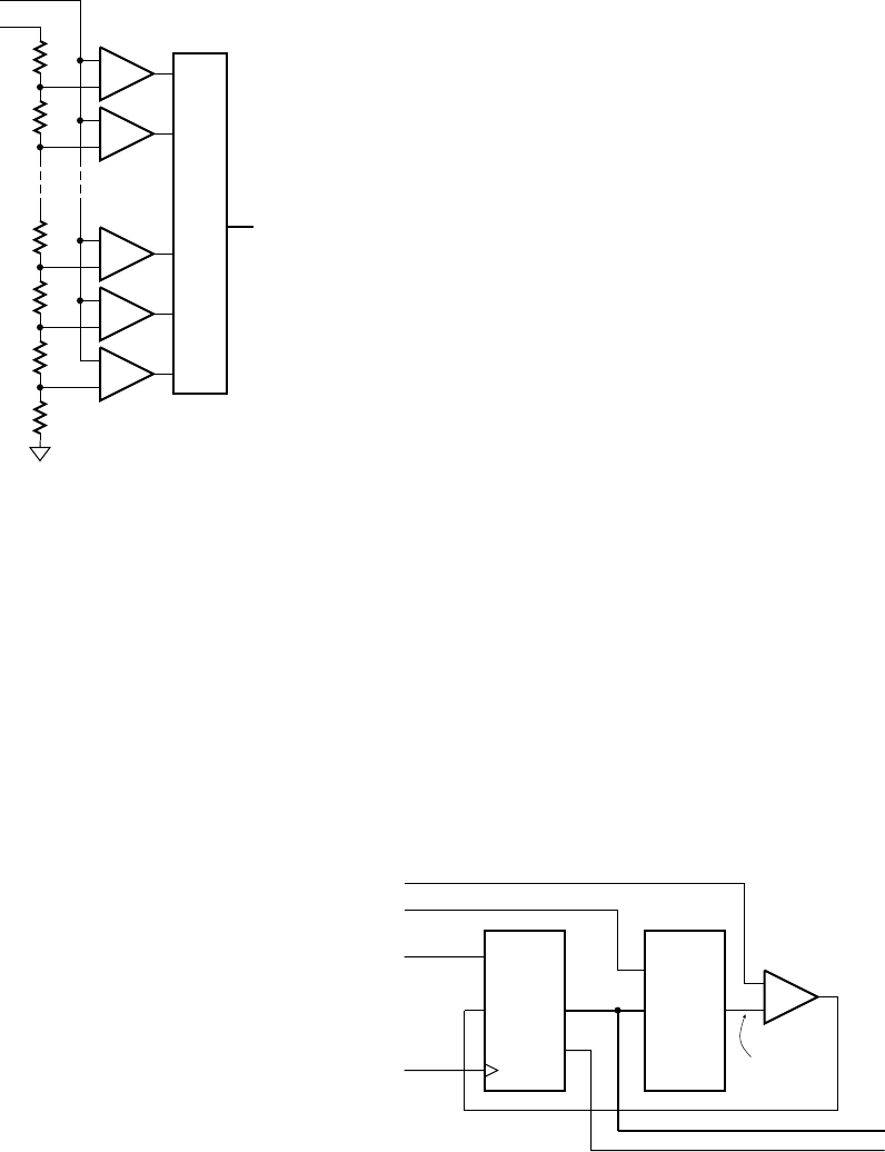
320 CHAPTER EIGHT i/o interfacing
The simplest form of ADC is a flash ADC, illustrated in Figure 8.5.
A converter with n output bits consists of a bank of 2
n
– 1 comparators
that compare the input voltage with reference voltages derived from a
voltage divider. For a given input voltage V
in
kV
f
, where V
f
is the full-
scale voltage and k is a fraction between 0.0 and 1.0, a proportion k of the
comparators have their reference voltage above V
in
and so output 1, and
the remaining comparators have their reference voltage lower than V
in
and so output 0. The comparator outputs drive the encoder circuit that
generates the fixed-point binary code for k. Flash ADCs have the advan-
tage that they convert an input voltage to digital form very quickly. High-
speed flash ADCs can perform tens or hundreds of millions of samples per
second, and so are suitable for converting high bandwidth signals such as
those from high-definition video cameras, radio receivers, radars, and so
on. Their disadvantage is that they need large numbers of comparators.
Hence, they are only practical for ADCs that encode the converted data
using a relatively small number of bits. Common flash ADCs generate
8 bits of output data. We say they have a resolution of 8 bits, correspond-
ing to the precision of the fixed-point format with which they represent
the converted signal.
For signals that change more slowly, we can use a successive approxi-
mation ADC, shown in Figure 8.6. It uses a digital-to-analog converter
(DAC) internally to make successively closer approximations to the input
signal over several clock periods. To illustrate how the ADC works, con-
sider a converter that produces an 8-bit output. When start input is acti-
vated, the successive approximation register (SAR) is initialized to the
binary value 01111111. This value is provided to the DAC, which pro-
duces the first approximation, just less than half of the full-scale voltage.
The comparator compares this approximation with the input voltage. If
the input voltage is higher, the comparator output is 1, indicating that
a better approximation would be above the DAC output. If the input
voltage is lower, the comparator output is 0, indicating that a better
+
–
+
–
+
–
+
–
+
–
Vin
Vf
Encoder
FIGURE 8.5 A fl ash ADC.
+
–
DACSAR
Dout
done
Vin
Vf
start
clk
(analog)
(analog)
(analog)
FIGURE 8.6 A successive
approximation ADC. Analog
signals are indicated; the
remaining signals are digital.
approximation would be below the DAC output. The comparator output
is stored as the most significant bit in the SAR, and remaining bits are
shifted down one place. This gives the next approximation, d
7
0111111,
which is either one-quarter or three-quarters of the full-scale voltage,
depending on d
7
. During the next clock period, this next approximation
is converted by the DAC and compared with the input voltage to yield
the next most significant bit of the result and a refined approximation,
d
7
d
6
011111. The process repeats over successive clock cycles, refining the
approximation by one bit each cycle. When all bits of the result are deter-
mined, the SAR activates the done output, indicating that the complete
result can be read.
The advantage of a successive approximation ADC over a flash
ADC is that it requires significantly fewer analog components: just one
comparator and a DAC. These components can be made to high precision,
giving a high-precision ADC. 12-bit successive approximation ADCs, for
example, are commonly available. The disadvantage, however, is that
more time is required to convert a value. If the input signal changes by
more than the precision of the ADC while the ADC is making successive
approximation, we need to sample and hold the input. This requires a
circuit that charges a capacitor to match the input voltage during a brief
sampling interval, and then maintain the voltage on the capacitor while it
is being converted. Another disadvantage of the successive approximation
ADC is the amount of digital circuitry required to implement the SAR.
However, that function could be implemented on an embedded processor,
requiring just an output register to drive the DAC and an input bit from
the comparator. The sequencing of successive approximations would then
form part of the embedded software.
There are other forms of ADC apart from flash and successive
approximation ADCs, each with advantages and disadvantages. Choice
among them depends on the resolution, conversion speed and other
factors dictated by the application. In practice, there is often a need to
filter the analog input signal to ensure correct conversion to digital form.
These considerations are beyond the scope of this book. More details can
be found in books on digital signal processing mentioned in the Further
Reading section.
8.1.2 OUTPUT DEVICES
Among the most common output devices are indicator lights that display
on/off or true/false information. For example, an indicator might show
whether a mode or operation is active, whether the system is busy, or
whether an error condition has occurred. The simplest form of indicator
is a single light-emitting diode (LED). It is low in cost, highly reliable,
and easy to drive from a digital circuit, as Figure 8.7 shows. When the
output from the driver is a low voltage, current flows through the LED,
8.1 I/O Devices CHAPTER EIGHT 321
output
driver
+V
FIGURE 8.7 Output circuit
for an LED indicator.

322 CHAPTER EIGHT i/o interfacing
causing it to turn on. The resistor limits the current so as not to overload
the output driver or the LED. We choose the resistance value to deter -
mine the current, and hence the brightness of the LED. When the output
from the driver is a high voltage (near the supply voltage), the voltage
drop across the LED is less than its threshold voltage, so no current flows;
hence, the LED is turned off. We could, alternatively, connect the LED
and resistor to ground, allowing a high output voltage to turn on the LED
and a low output voltage to turn it off. However, output circuits designed
to drive TTL logic levels are better able to sink current in the low state
than to source current in the high state. Thus, it is more common to con-
nect an LED as shown in Figure 8.7.
example 8.1 Determine the resistance for an LED pull-up resistor
connected to a 3.3V power supply. The LED has a forward-biased voltage drop
of 1.9V, and is suffi ciently bright with a current of 2mA.
solution Assuming the output driver low voltage is close to 0V, the volt-
age drop across the resistor must be 3.3V 1.9V 1.4V. Using Ohm’s Law with
a current of 2mA means the resistance must be 1.4/0.002 700Ω. The closest
standard value is 680Ω.
Displays
In Section 2.3.1, we introduced 7-segment displays and showed how we
could decode a BCD value to drive the seven segments of a digit. In many
applications, we have several digits to display. For example, an alarm
clock typically has four digits for the hours and minutes of the time. While
we could decode and drive each digit individually, that would require
numerous output drivers, package pins and signals for the interconnec-
tions. Usually, it is more cost effective to connect the anodes or the cath-
odes of the LEDs for each digit in common, and to scan the digits. The
connections for the LEDs in each digit, in this case, with common anodes,
are shown in Figure 8.8. In addition to the seven LEDs for the segments,
there is an LED for a decimal point (dp). The output connections for four
digits are shown in Figure 8.9. Each of the outputs
__
A0 through
__
A3 , when
pulled low, turns on the transistor that enables a digit. We usually need
these external transistors, since IC outputs cannot source enough current
to drive up to eight LEDs directly.
To display four digits, we pull each of
__
A0 through
__
A3 low in turn.
When
__
A0 is low, enabling the least significant digit, we drive the segment
lines,
_
a though
_
g and
__
dp , low or high as required for the segment pattern
for that digit. When
__
A1 is low, we drive the segment lines for the next
digit, and so on. After driving the most significant digit, we cycle back to
the least significant digit. If we cycle through the digits fast enough, our
a
b
c
d
e
f
g
dp
common
anode
FIGURE 8.8 Connection
of segment LEDs in a common
anode 7-segment display.
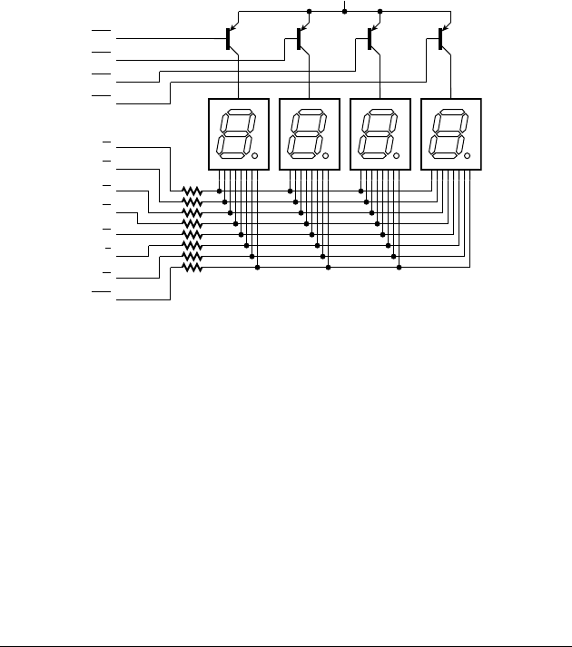
eyes’ persistence of vision smooths out any flickering due to each digit
only being active 25% of the time.
The advantage of this scanned scheme is that we only need one signal for
each digit plus one for each segment of a digit. For example, to drive four dig-
its, we need 12 signals, compared with the 32 signals we would need had we
driven segments individually. Depending on our application, we might use a
counter or a shift register to drive the digit enable outputs and an 8-bit-wide
multiplexer to select the values to drive onto the segment outputs. Often,
however, the display is controlled by an embedded processor. In that case, we
can simply provide output registers for the digit and segment outputs and let
the embedded software manage the sequencing of output values.
example 8.2 Develop a Verilog model of a display multiplexer and
decoder for the 4-digit 7-segment display shown in Figure 8.9. The circuit has
four BCD inputs. The decimal point for the left-most digit should be lit, and the
remaining decimal points not lit. The system clock has a frequency of 10MHz.
solution The module for the circuit has ports for the clock, reset and
BCD inputs and for the the segment and anode outputs. Element 7 of the
segment output drives the decimal point segment, and elements 6 down to 0
drive segments g through a, respectively. The outputs all use active-low logic.
The circuit must include a multiplexer that selects each of the BCD inputs in
turn. It decodes it to drive the 7-segment cathodes at the same time as acti-
vating the anode for the selected digit. Since we are relying on persistence of
vision to avoid perceptible flicker, we need to cycle through the digits so that
each is activated sufficiently frequently. A 50Hz cycle rate is acceptable. We
A3
A2
A1
A0
a
b
c
d
e
f
g
dp
+V
FIGURE 8.9 Connection of
four 7-segment display digits.
8.1 I/O Devices
CHAPTER EIGHT 323

324 CHAPTER EIGHT i/o interfacing
can achieve that rate by dividing the 10MHz clock down to 200Hz to activate
a 2-bit counter for selecting digits. A module to implement these design
decisions is
module display_mux ( output reg [3:0] anode_n,
output [7:0] segment_n,
input [3:0] bcd0, bcd1, bcd2, bcd3,
input clk, reset );
parameter clk_freq = 10000000;
parameter scan_clk_freq = 200;
parameter clk_divisor = clk_freq / scan_clk_freq;
reg scan_clk;
reg [1:0] digit_sel;
reg [3:0] bcd;
reg [7:0] segment;
integer count;
// Divide master clock to get scan clock
always @(posedge clk)
if (reset) begin
count = 0;
scan_clk <= 1'b0;
end
else if (count = = clk_divisor — 1) begin
count = 0;
scan_clk <= 1'b1;
end
else begin
count = count + 1;
scan_clk <= 1'b0;
end
// increment digit counter once per scan clock cycle
always @(posedge clk)
if (reset) digit_sel <= 2'b00;
else if (scan_clk) digit_sel <= digit_sel + 1;
// multiplexer to select a BCD digit
always @*
case (digit_sel)
2'b00: bcd = bcd0;
2'b01: bcd = bcd1;
2'b10: bcd = bcd2;
2'b11: bcd = bcd3;
endcase
(continued)

// activate selected digit's anode
always @*
case (digit_sel)
2'b00: anode_n = 4'b1110;
2'b01: anode_n = 4'b1101;
2'b10: anode_n = 4'b1011;
2'b11: anode_n = 4'b0111;
endcase
// 7-segment decoder for selected digit
always @*
case (bcd)
4'b0000: segment[6:0] = 7'b0111111; // 0
4'b0001: segment[6:0] = 7'b0000110; // 1
4'b0010: segment[6:0] = 7'b1011011; // 2
4'b0011: segment[6:0] = 7'b1001111; // 3
4'b0100: segment[6:0] = 7'b1100110; // 4
4'b0101: segment[6:0] = 7'b1101101; // 5
4'b0110: segment[6:0] = 7'b1111101; // 6
4'b0111: segment[6:0] = 7'b0000111; // 7
4'b1000: segment[6:0] = 7'b1111111; // 8
4'b1001: segment[6:0] = 7'b1101111; // 9
default: segment[6:0] = 7'b1000000; // "-"
endcase
// decimal point is only active for digit 3
always @* segment[7] = digit_sel = = 2'b11;
// segment outputs are negative logic
assign segment_n = ~segment;
endmodule
The first always block is the clock divider that generates the 200Hz clock for
selecting digits. It sets the variable
scan_clk to 1 for one master clock cycle at a
200Hz rate. The second always block implements the 2-bit counter, incrementing
the
digit_sel variable each time scan_clk is 1. The next two always blocks use the
digit_sel signal to select the BCD digit and to activate the corresponding anode.
The remaining always block and assignments decode the selected digit to drive
the segment cathodes.
As an alternative to using LEDs for displays, some systems use liquid
crystal displays (LCDs). Each segment of an LCD consists of liquid crystal
material between two optical polarizing filters. The liquid crystal also
polarizes light, and, depending on the angle of polarization, can allow
light to pass or be blocked by the filters. The liquid crystal is forced to
twist or untwist, thus changing its axis of polarization, by application of
a voltage to electrodes in front of and behind the segment. By varying the
8.1 I/O Devices CHAPTER EIGHT 325
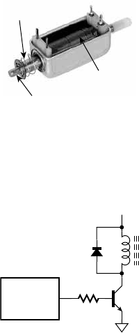
326 CHAPTER EIGHT i/o interfacing
voltage, we can make the segment appear transparent or opaque. Thus,
LCDs require ambient light to be visible. In low light conditions, a back
light is needed, which is one of their main disadvantages. The other disad-
vantages include their mechanical fragility and the smaller range of tem-
peratures over which they can operate. They have several advantages over
LEDs, including readability in bright ambient light conditions, very low
power consumption, and the fact that custom display shapes can readily
be manufactured.
Seven-segment displays are useful for applications that must display a
small amount of numeric information. However, more complex applica-
tions often need to display alphanumeric or graphical information, and
so may use LCD display panels. These can range from small panels that
can display a few characters of text, to larger panels that can display text
or images up to 320 240 dots, called pixels (short for picture elements).
Beyond that size, systems would typically use the same kinds of display
panels that are used in general purpose PCs. Since output for display pan-
els is much more involved than output for simple segment-based displays,
more complex control circuits are needed. We will return to control of
display panels in Section 8.2.
Electromechanical Actuators and Valves
One of the simplest forms of actuator used to cause mechanical effects is a
solenoid, shown in Figure 8.10. With no current flowing through the coil,
the spring holds the steel armature out from the coil. When current flows,
the coil acts as an electromagnet and draws the armature in against the
spring. In a digital system, we can control the current in a small solenoid
with a transistor driven by a digital output signal, as shown in Figure 8.11.
The diode is required to absorb the voltage spikes that arise when the cur-
rent through the inductive load is turned off.
The direct mechanical effect of activating a solenoid is a small linear
movement of the armature. We can translate this into a variety of other
effects by attaching rods and levers to the armature, allowing us to control
the operation of mechanical systems. Hence, digitally controlled solenoids
are widely used in manufacturing and other industrial applications.
There are two important classes of devices based on solenoids, the
first being solenoid valves. We can attach the armature of a solenoid to a
valve mechanism, allowing the solenoid to open and close the valve, thus
regulating the flow of a fluid or gas. This gives us a means of controlling
chemical processes and other fluid or gas based processes. Importantly,
a hydraulic solenoid valve (controlling flow of hydraulic fluid) or a pneu-
matic solenoid valve (controlling flow of compressed air) can be used
to indirectly control hydraulic or pneumatic machinery. Such machines
can operate with much greater force and power than electrical machines.
So solenoid valves are important components in the interface between
coil
spring
armature
FIGURE 8.10 A solenoid
actuator.
output
driver
+V
FIGURE 8.11 Solenoid
controlled by a digital output.
the disparate low-power digital electronic domain and the high-power
mechanical domain.
The second class of device based on solenoids is relays. In these
devices, the armature is attached to a set of electrical contacts. This allows
us to open or close an external circuit under digital control. The reasons
for using a relay are twofold. First, the external circuit can operate with
voltages and currents that exceed those of the digital domain. For exam-
ple, a home automation system might use a relay to activate mains power
to a mains powered appliance. Second, a relay provides electrical isolation
between the controlling and the controlled circuit. This can be useful if the
controlled circuit operates with a different ground potential, or is subject
to significant induced noise.
Motors
Whereas solenoids allow us to control a mechanical effect with two states,
many applications require mechanical movement over a range of positions
and at varying speeds. For these applications, we can use electric motors
of various kinds, including stepper motors and servo motors. Both can be
used to drive shafts to controlled positions or speeds. The rotational posi-
tion or motion can be converted to linear position or motion using gears,
screws, and similar mechanical components.
A stepper motor is the simpler of the two kinds of motors that
we can control with a digital system. Its operation is shown in simplified
form in Figure 8.12. The motor consists of a permanent magnet rotor
mounted on the shaft. Surrounding the rotor is a stator with a number
of coils that can be energized to form electromagnetic poles. The figure
shows that, as coils are energized in sequence, the rotor is attracted to
successive angular positions, stepping around through one rotation. The
magnetic attraction holds the rotor in position, provided there is not too
much opposing torque from the load connected to the motor shaft. The
order and rate in which the coils are energized determines the direction
and speed of rotation.
NN
SS
NNSSN S
N
S
NS
N
S
NN
SS
NN SS
FIGURE 8.12 Operation of a
stepper motor.
8.1 I/O Devices
CHAPTER EIGHT 327
328 CHAPTER EIGHT i/o interfacing
Practical stepper motors have more poles around the stator, allowing
the motor to step with finer angular resolution. They also have varying
arrangements of coil connections, allowing finer control over stepping.
In practical applications, current through the coils is switched in either
direction using transistors controlled by digital circuit outputs. The fact
that the motor is activated by the on/off switching of current makes
stepper motors ideal for digital control.
A servo-motor, unlike a stepper motor, provides continuous rotation.
The motor itself can be a simple DC motor, in which the applied voltage
determines the motor’s speed, and the polarity of the applied voltage
determines the direction of rotation. The “servo” function of the motor
involves the use of feedback to control the position or speed of the motor.
If we are interested in controlling position, we can attach a position sensor
to the motor shaft. We then use a servo controller circuit that compares
the actual and desired positions, yielding a drive voltage for the motor that
depends on the difference between the positions. If we are interested in
controlling the speed, we can attach a tachometer (a speed sensor) to the
shaft, and again use a comparator to compare actual and desired speed to
yield the motor drive voltage. In both cases, we can implement the servo
controller as a digital circuit or using an embedded processor. We need a
digital-to-analog converter to generate the drive voltage for the motor. We
can use various position or speed sensors, including the position encoders
we discussed in Sections 3.1.3 and 8.1.1.
Realistic servo control involves fairly complex computations to com-
pensate for the nonideal characteristics of the motor and any gearbox
and other mechanical components, as well as dealing with the effects of
the mechanical load on the system. We won’t go into any detail of those
effects in this book.
Digital-to-Analog Converters
Digital-to-analog converters (DACs) are the complement of analog-to-digital
converters. A DAC takes a binary-encoded number and generates a voltage
proportional to the number. We can use the voltage to control analog output
devices, such as the servo motors we described above, loudspeakers, and
so on.
One of the simplest forms of DAC is an R-string DAC, shown in
Figure 8.13. Like the flash ADC, it contains a voltage divider formed with
precision resistors. The binary-encoded digital input is used to drive a mul-
tiplexer formed from analog switches, selecting the voltage corresponding
to the encoded number. The selected voltage is buffered using a unity-
gain analog amplifier to drive the final output voltage. This form of DAC
works well for a small number of input bits, since it is possible to match
the resistances to achieve good linearity. However, for a larger number
of input bits, we require an exponentially larger number of resistors and
switches. This scheme becomes impractical for DACs with more than
eight to ten input bits.
An alternative scheme is based on summing of currents in resistor
networks. One way of doing this is shown in Figure 8.14, sometimes
called an R/2R ladder DAC. Each of the switches connected to the input
bits connects the 2R resistance to the reference voltage Vf if the input is
1, or to ground if the input is 0. While the analysis is beyond the scope of
this book, it can be shown that the currents sourced into the input node of
the op-amp when the switches are in the 1 position are binary weighted.
Those switches in the 0 position source no current. The superposition of
the sourced currents means that the total current is proportional to the
binary coded input. The op-amp voltage is thus also proportional to the
binary coded input, in order to maintain the virtual ground at the op-amp
input.
Just as there are numerous forms of analog-to-digital converter with
various advantages and disadvantages, there are similarly numerous forms
of digital-to-analog converter. We would choose an appropriate converter
to meet the cost, performance and other constraints that apply to each
Vf
R
R
R
R
R
R
R
R
Vout
a(0) a(1) a(2)
FIGURE 8.13 An R-string
DAC.
8.1 I/O Devices
CHAPTER EIGHT 329
330 CHAPTER EIGHT i/o interfacing
application. More detail can be found in books on digital signal process-
ing mentioned in the Further Reading section.
1. What is a sensor? What is an actuator?
2. Why would a digital system require a digital-to-analog converter?
3. How would we tell whether the 6 key in the keypad of Figure 8.1 is
pressed?
4. Given the incremental encoder of Figure 8.3, if B is 1 when a 0 to 1
transition occurs on A, in which direction is the shaft rotated?
5. How many comparators are required in a fl ash ADC with a
resolution of 8 bits?
6. How can we reduce the number of connections required for a
multidigit 7-segment LED display?
7. What is the difference between a solenoid and a relay?
8. Identify two kinds of motor that we might control with a digital
system.
9. If an application requires a 12-bit digital-to-analog converter (DAC),
would we choose an R-string DAC or an R/2R ladder DAC? Why?
8.2 I/O CONTROLLERS
Given transducers, analog-to-digital converters and digital-to-analog
converters, we can construct digital systems that include circuits to
KNOWLEDGE
TEST QUIZ
KNOWLEDGE
TEST QUIZ
Vf 2R
R
2R
R
R
2R
2R
2R
2R
Vout
a(3)
a(2)
a(1)
a(0)
+
–
FIGURE 8.14 An R/2R
ladder DAC.
process the converted input information in digital form to yield output
information. However, for an embedded computer to make use of the
information, we need to include components that allow the embedded
software to read input information and to write output information.
For dealing with input, we can provide an input register whose con-
tent can be loaded from the digital input data and that can be read in
the same way that the processor reads a memory location. For dealing
with output, we can provide an output register that can be written by
the processor in the same way that it writes to a memory location. The
output signals of the register provide the digital information to be used
by the output transducer. Many embedded processors refer to input and
output registers as ports. Since it is such a commonly used term, we will
make use of it, and take care to avoid confusion with ports of Verilog
modules.
In practice, both input and output registers are parts of input and
output controllers that govern other aspects of dealing with transducers
under software control. We will start our discussion of I/O controllers in
this section with some simple controllers that just include input and out-
put registers for transferring data. We will then move on to consider more
advanced controllers.
8.2.1 SIMPLE I/O CONTROLLERS
The simplest form of controller consists just of an input register that
captures the data from an input device, or just an output register to provide
data to a device. Usually, there are several I/O registers, so we need to
select which register to read from or write to. This is similar to selecting
which memory location to access, and is solved in the same way, namely
by providing each register with an address. When the embedded proces-
sor needs to access an input or output register, it provides the address of
the required register. We decode the address to select the register, and only
enable reading or writing of that register.
As we mentioned in Chapter 7, some processors use memory mapped
I/O; that is, they just use certain memory addresses to refer to I/O reg-
isters and use the same load and store instructions for accessing both
memory location and I/O registers. We can use address decoding circuits
connected to the processor to identify whether memory or I/O registers
are being accessed, and enable the memory chips or the appropriate reg-
ister as required. Other processors, like the Gumnut that we described
in Chapter 7, have separate address spaces for memory and I/O regis-
ters, and include special instructions for reading and writing I/O registers.
They provide control signals that distinguish between memory and I/O
register access.
8.2 I/O Controllers CHAPTER EIGHT 331
332 CHAPTER EIGHT i/o interfacing
example 8.3 The signals provided by the Gumnut core for connecting to
I/O registers are described in the following Verilog module defi nition:
module gumnut ( input clk_i,
input rst_i,
...
output port_cyc_o,
output port_stb_o,
output port_we_o,
input port_ack_i,
output [7:0] port_adr_o,
output [7:0] port_dat_o,
input [7:0] port_dat_i,
... );
endmodule
The output port_adr_o is the port address, port_dat_o is the data written by an
out instruction, port_dat_i is the data read by an inp instruction, port_cyc_o
and
port_stb_o indicate that a port read or write operation is to be performed,
port_we_o indicates that the operation is a write, and port_ack_i indicates that
the selected port is ready and has acknowledged completion of the read or write
operation.
Develop a controller for the keypad matrix shown in Figure 8.2, and show how
to connect the controller to a Gumnut core. Use output port address 4 for the
matrix row output register and input port address 4 for the matrix column input
register.
solution The controller connects to the Gumnut I/O signals on one
side and to the keypad row and column signals on the other side, as shown in
Figure 8.15. We decode the port address from the Gumnut core externally to the
controller to derive the strobe control signal (
stb_i) for the controller.
port_dat_i
port_ack_i
port_adr_o
port_we_o
port_cyc_o
Gumnut
port_dat_o
port_stb_o stb_i
dat_i
cyc_i
we_i
Keypad Controller
dat_o
keypad_row
keypad_col
ack_o=
keypad_port_
addr
123
456
789
*0#
FIGURE 8.15 Connection
of a Gumnut core to a keypad
controller.

The Verilog module definition for the controller is
module keypad_controller ( input clk_i,
input cyc_i,
input stb_i,
input we_i,
output ack_o,
input [7:0] dat_i,
output reg [7:0] dat_o,
output reg [3:0] keypad_row,
input [2:0] keypad_col );
reg [2:0] col_synch;
always @(posedge clk_i) // Row register
if (cyc_i && stb_i && we_i) keypad_row <= dat_i[3:0];
always @(posedge clk_i) begin // Column synchronizer
dat_o <= {5'b0, col_synch};
col_synch <= keypad_col;
end
assign ack_o = cyc_i && stb_i;
endmodule
The first always block represents the keypad row output register, storing the
value to drive on the keypad row outputs. The second always block represents
the keypad column input register. Since the key switches may change at any time,
we need to synchronize the input with the clock to avoid metastability failures.
(We discussed this issue in Section 4.4.1.) In this design, we assume the keypad
controller is the only thing driving the
port_dat_o outputs, so we can assign
directly to them regardless of the state of the control inputs. We will return to
the topic of connecting multiple controllers in Section 8.3. The final assignment
in the architecture body activates the
port_ack_o output immediately on any port
read or write operation, since there is no need to make the processor wait.
The controller is connected to a Gumnut core in an embedded system as shown
in the following module outline:
module embedded_system;
wire ...
parameter [7:0] keypad_port_addr = 8
'h04;
8.2 I/O Controllers CHAPTER EIGHT 333
(continued)

334 CHAPTER EIGHT i/o interfacing
wire keypad_stb_o;
gumnut processor_core
( .clk_i(clk), .rst_i(rst), ...,
.port_cyc_o(port_cyc_o), .port_stb_o(port_stb_o),
.port_we_o(port_we_o), .port_ack_i(port_ack_i),
.port_adr_o(port_adr_o), .port_dat_o(port_dat_o),
.port_dat_i(port_dat_i), ... );
assign keypad_stb_o = port_adr_o
== keypad_port_addr & port_stb_o;
keypad_controller keypad
( .clk_i(clk),
.cyc_i(port_cyc_o), .stb_i(keypad_stb_o),
.we_i(port_we_o), .ack_o(port_ack_i),
.dat_i(port_dat_o), .dat_o(port_dat_i),
.keypad_row(keypad_row), .keypad_col(keypad_col) );
endmodule
The assignment to keypad_stb_o compares the Gumnut I/O port address with
the value allocated for the keypad controller registers to derive the strobe signal
for the keypad controller. The data input and output signals and the other con-
trol signals connect directly between the core and the controller.
While a simple I/O controller just has registers for input and output of
data, more involved I/O controllers also have registers to allow the embed-
ded processor to manage operation of the controller. Such registers might
include control registers, to which a processor writes parameters govern-
ing the way transducers operate, and status registers, from which the pro-
cessor reads the state of the controller. We often require such registers
for controllers whose operation is sequential, since we need to synchronize
controller operation with execution of the embedded software. As a
consequence, we may have a combination of readable and writable regis-
ters used to control an input-only device or an output-only device.
example 8.4 In Section 8.1.1, we described a successive approximation
analog-to-digital converter. It produces a binary-coded value representing the
input voltage as a proportion of the full-scale reference voltage, V
f
. We also
mentioned that a sample-and-hold circuit can be used on the analog input if
the voltage can change during the conversion process. Design a controller for
a successive approximation ADC to connect to the Gumnut processor core.
The controller has a control register whose contents govern operation of the
converter. Bits 0 and 1 select among four alternate full-scale reference voltages.
When a 1 is written to bit 2, the analog voltage is held and a conversion is
started; when a 0 is written to the bit, the analog voltage is tracked. The control-
ler also has a status register and an input data register. Bit 0 of the status register
is 1 when a conversion is complete, and 0 otherwise. Other bits of the register
are read as 0. The input data register contains the converted data.
solution The controller circuit is shown in Figure 8.16. The control
register is enabled when the least signifi cant port address bit is 1 during a port
write operation. The remaining port address bits are not decoded. Bits 0 and 1 of
the register are decoded to control four analog switches that select the reference
D2
CE
reset
Q2
D1 Q1
D0 Q0
clk
Y2
Y3
D1
Y1D0
Y0
start
reset
done
Vf
Dout
ADC
Vin
clk
0
1
0
0
Vin
port_dat_o
port_ack_o
Vf_0
Vf_1
Vf_2
Vf_3
port_dat_i
port_cyc_i
rst_i
clk_i
port_adr_i(0)
1
2
7...1
port_we_i
port_stb_i
port_cyc_i
port_stb_i
voltage. Bit 2 of the register controls the sample-and-hold component and the
start signal of the ADC. The least signifi cant port address bit is also used to
select between the ADC data value and the ADC
done status signal. Thus, when
the processor performs a port read at address 0, it reads the ADC data, and
when it performs a port read at address 1, it reads the
done status.
8.2.2 AUTONOMOUS I/O CONTROLLERS
The simple I/O controllers in the previous section either involve no
sequencing of operations, or just simple sequencing in response to accesses
by a processor. More complex I/O controllers, on the other hand, operate
autonomously to control the operation of an input or output device. For
example, a servo-motor controller, given the desired position in an output
register, might independently compute the difference between desired
and actual position, compensate for mechanical lead and lag, and drive
the motor accordingly. Interaction with the processor might only occur
FIGURE 8.16 Circuit for
a controller for a successive
approximation ADC.
8.2 I/O Controllers
CHAPTER EIGHT 335
336 CHAPTER EIGHT i/o interfacing
through the processor updating the desired position in the output register
and monitoring the position difference by reading an input register. In
some cases, if an autonomous controller detects an event of interest to the
embedded software, for example, an error condition, the controller must
notify the processor. We will discuss interrupts as a means of doing this
in Section 8.5.2.
One reason for providing autonomy in the controller is that it allows
the processor to perform other tasks concurrently. This increases the
overall performance of the system, though at the cost of the additional cir-
cuitry required for the controller. Another reason is to ensure that control
operations are performed fast enough for the device. If the device needs
to transfer data at high rates, or needs control operations to be performed
without delay, a small embedded processor may not be able to keep up.
Making the I/O controller more capable may be a better trade-off than
increasing the performance or responsiveness of the processor.
As an illustration of an autonomous controller, let us return to the
LCD display panels that we mentioned in Section 8.1.2 as a form of out-
put device for complex digital systems. LCD panels consist of a rectan-
gular array of liquid crystal pixels. The electrodes are connected in rows
on one side of the panel and in columns on the other side. A voltage is
applied to one row at a time, and the column electrodes are variously set
to the same or a complementary voltage to activate pixels in the selected
row. In this way, the panel is scanned row by row to refresh the pixel
states, in much the same way that a dynamic memory must be refreshed.
Since managing and refreshing an LCD panel requires a lot of activity,
manufacturers of panels typically combine a display controller with a
panel to form an LCD module. The display controller is an autonomous
digital subsystem that includes memory for storing the information to be
displayed on the panel and circuitry for refreshing the panel. An embed-
ded computer treats the display controller as a specialized output control-
ler, and provides it with updates to the stored information. In a graphical
LCD module, the stored information consists of the image to be displayed,
represented with one bit per pixel. In a character LCD module, the stored
information consists of the binary code words for the characters. The dis-
play controller is responsible for decoding the character code words and
rendering the image corresponding to the characters.
A specific example of an LCD module is the ASI-D-1006A-DB-_S/
W module from All Shore Industries, Inc., a 100 60 pixel LCD panel
that includes an SED1560 controller chip from Seiko Epson Corp. The
module is designed to connect to 8-bit microcontrollers, such as the 8051
that we mentioned in Chapter 7. Figure 8.17 shows how this might be
done. The controller chip has an internal memory for storing the image
to be displayed on the LCD panel. The chip provides a control register to
which the microcontroller can write encoded commands, a status register,
and a data input/output register for access to the display memory. The
microcontroller issues commands to the chip to configure the display and
to load pixel data into the memory. Thereafter, the chip autonomously
manages scanning the display using the pixel data in its memory, leaving
the microcontroller free to perform other tasks.
As we mentioned above, the use of an autonomous controller may be
appropriate for a device that must transfer input or output data at high
rates. Often, such data must be written to memory (in the case of input
data) or read from memory (in the case of output data). If the data trans-
fer were done by a program copying data between memory and controller
registers, that activity would consume much of the processor’s time. An
alternative, commonly adopted in high-speed autonomous controllers, is to
use direct memory access (DMA), in which the controller reads data from
memory or writes data to memory without intervention by the processor.
The processor provides the starting memory address to the controller (by
writing the address to a control register), and the controller then performs
the data transfer autonomously. We can think of a controller that oper-
ates in this way as an accelerator for input/output operations. Since other
forms of accelerator also use DMA for data transfer, we will defer a more
detailed description of DMA until Chapter 9.
1. What is the purpose of an input register in an I/O controller? What
is the purpose of an output register?
2. What is the purpose of a control register in an I/O controller? What
is the purpose of a status register?
3. If an embedded processor uses memory mapped I/O, how do we
distinguish accesses to memory from accesses to I/O registers?
KNOWLEDGE
TEST QUIZ
KNOWLEDGE
TEST QUIZ
A(0)
CS1
C86
P/S
WR
RD
D
CS2
P2(0)
PSEN
ALE
RESET
8051 LCD Module
RD
WR
P0
RST
+V
FIGURE 8.17 An LCD
module connected to an 8051
microcontroller.
8.2 I/O Controllers
CHAPTER EIGHT 337
338 CHAPTER EIGHT i/o interfacing
4. Why might a controller for an input device have registers to which a
processor can write?
5. What advantages do autonomous I/O controllers have over simple
controllers?
8.3 PARALLEL BUSES
As we have seen, digital circuits consist of various interconnected com-
ponents. Each component performs some operation or stores data. The
interconnections are used to move data between the components. Where
the data is binary coded, several signals are connected in parallel, one
per bit of the encoding. Many of the interconnections we have seen thus
far have been simple point-to-point connections, with one component as
the source of data and a single separate component as the destination. In
other cases, connections fan out from a single source to multiple destina-
tions, allowing each of the destination components to receive data from
the source.
In some systems, especially embedded systems containing proces-
sor cores, parallel connections carry encoded data from multiple sources
to several alternate destinations. Such connection structures, shown
conceptually in Figure 8.18, are called buses. In the simplest case, a
bus is just the collection of signals carrying the data, and control remains
in a separate control section that sequences operation of the data
sources and destinations. In more elaborate buses, data sources and
destinations are autonomous, each with its own control section. In
such cases, the control sections must communicate to synchronize the
transfer of data. They do so using control signals that form part of the
bus structure.
While the bus structure shown in Figure 8.18 shows the general idea
of bus connection structures, it is not realizable directly as shown. Since
the bus signals are shared between the data sources, only one of them
should provide data at once. Most of the circuit components that we have
considered so far always drive either a low or a high logic level at their
outputs. If one data source drives a low level while another drives a high
level, the resulting conflict would cause large currents to flow between the
two components, possibly damaging them. There are several solutions to
this problem, and we will look at them in turn.
8.3.1
MULTIPLEXED BUSES
One solution is to use a multiplexer to select among the data sources, as
shown in Figure 8.19. The multiplexer selects the value to drive the bus
signals based on a control signal generated by a control section. If the
bus has n data sources, an n-input multiplexer is required for each bit of
data
source
data
destination
data
source
data
destination
data
destination
FIGURE 8.18 Conceptual
connection structure for a bus.
the encoded data transmitted over the bus. Depending on the number of
sources and the arrangement of the components and signals on the inte-
grated circuit chip, the multiplexer may be implemented as a single n-input
multiplexer, or it may be subdivided into sections distributed around the
chip. For example, if a bus has five data sources, two of which are on one
side of a chip and the remaining three are on the other side, the bus wiring
may be simplified by using a 2-input multiplexer adjacent to the two data
sources and a 3-input multiplexer adjacent to the three data sources. The
outputs of the multiplexers would then be connected to a 2-input multi-
plexer adjacent to the data destinations.
One extreme form of subdivision of bus multiplexers is the fully
distributed structure shown in Figure 8.20. The data signals are con-
nected in a chain going past all of the sources and then routed to the desti-
nations. Each multiplexer either connects its associated data source to the
chain (when the multiplexer’s select input is 1) or forwards data from a
preceding source (when the select input is 0). The advantage of this form
of distributed multiplexer is the reduction in wiring complexity. It is often
easier to route a set of signals in a chain past circuit blocks rather than
trying to connect several data sources to a central hub.
One example of a bus designed to use multiplexers is the Wishbone
bus. The signals in the bus and their timing are specified in a standard
document, referenced in the Further Reading section. The Gumnut core
data
source
data
destination
data
source
data
destination
data
destination
0
1
FIGURE 8.19 A bus using a
multiplexer to select among data
sources.
FIGURE 8.20 A distributed-
multiplexer bus structure.
data
source
data
destination
data
source
data
destination
data
destination
1
0
1
0
data
source
1
0
data
source
8.3 Parallel Buses CHAPTER EIGHT 339
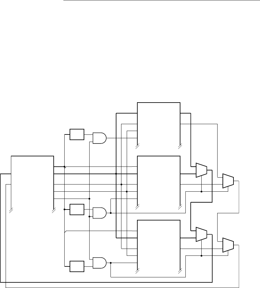
340 CHAPTER EIGHT i/o interfacing
uses a simple form of Wishbone bus for each of the instruction, data and
I/O port connections. The signals with a “_o” suffix are outputs from
a component, and the signals with a “_i” suffix are inputs. Where mul-
tiple “_o” signals are to be connected to a “_i” signal, a multiplexer is
required.
example 8.5 Show how, in an embedded system using a Gumnut core,
the keypad controller of Example 8.3 and two instances of the ADC controller of
Example 8.4, the components are interconnected using distributed multiplexers.
solution The Gumnut core is the single source for the port address and
control signals and for the output data signals, so no multiplexer is needed
for those signals. The controllers each provide input data and
ack signals, so
distributed multiplexers are needed for them. We can decode the port address to
derive the controller strobe signals and multiplexer select signals. We choose the
first ADC controller when the port address is 0 or 1, the second ADC when the
port address is 2 or 3, and the keypad controller when the port address is 4. The
connections are shown in Figure 8.21.
port_dat_i
port_ack_i
port_adr_o
port_we_o
port_cyc_o
Gumnut
port_dat_o
port_stb_o
adr_i(0)
dat_i
cyc_i
we_i
ADC Controller
dat_o
ack_o
stb_i
adr_i(0)
dat_i
cyc_i
we_i
ADC Controller
dat_o
ack_o
stb_i
stb_i
dat_i
cyc_i
we_i
Keypad Controller
dat_o
ack_o
0
1
0
1
0
1
0
1
= 0...1
= 2...3
= 4
0
0
FIGURE 8.21 Connection of
two ADC controllers and a keypad
controller to a Gumnut core using
distributed multiplexers.

example 8.6 Develop a Verilog model for the embedded system of
Example 8.5.
solution The module definition is
module embedded_system_ADC_keypad;
wire ...
parameter [7:0] ADC0_port_addr = 8'h00,
ADC1_port_addr = 8'h02,
keypad_port_addr = 8'h04;
wire ADC0_stb_o, ADC1_stb_o, keypad_stb_o;
wire [7:0] ADC0_dat_o, ADC1_dat_o, keypad_dat_o,
ADC0_dat_fwd, ADC1_dat_fwd;
wire ADC0_ack_o, ADC1_ack_o, keypad_ack_o,
ADC0_ack_fwd, ADC1_ack_fwd;
gumnut processor_core
( .clk_i(clk), .rst_i(rst), ...,
.port_cyc_o(port_cyc_o), .port_stb_o(port_stb_o),
.port_we_o(port_we_o), .port_ack_i(ADC1_ack_fwd),
.port_adr_o(port_adr_o), .port_dat_o(port_dat_o),
.port_dat_i(ADC1_dat_fwd), ... );
assign ADC0_stb_o = (port_adr_o & 8'hFE)
== ADC0_port_addr & port_stb_o;
assign ADC1_stb_o = (port_adr_o & 8'hFE)
== ADC1_port_addr & port_stb_o;
assign keypad_stb_o = port_adr_o
== keypad_port_addr & port_stb_o;
keypad_controller keypad ( .clk_i(clk),
.cyc_i(port_cyc_o),
.stb_i(keypad_stb_o),
.we_i(port_we_o),
.ack_o(keypad_ack_o),
.dat_i(port_dat_o),
.dat_o(keypad_dat_o), ... );
ADC_controller ADC0 ( .clk_i(clk), .rst_i(rst),
.cyc_i(port_cyc_o), .stb_i(ADC0_stb_o),
.we_i(port_we_o), .ack_o(ADC0_ack_o),
.adr_i(port_adr_o[0]), .dat_i(port_dat_o),
.dat_o(ADC0_dat_o), ... );
assign ADC0_dat_fwd = ADC0_stb_o ? ADC0_dat_o : keypad_dat_o;
assign ADC0_ack_fwd = ADC0_stb_o ? ADC0_ack_o : keypad_ack_o;
(continued)
8.3 Parallel Buses CHAPTER EIGHT 341
342 CHAPTER EIGHT i/o interfacing
ADC_controller ADC1 ( .clk_i(clk), .rst_i(rst),
.cyc_i(port_cyc_o), .stb_i(ADC1_stb_o),
.we_i(port_we_o), .ack_o(ADC1_ack_o),
.adr_i(port_adr_o[0]), .dat_i(port_dat_o),
.dat_o(ADC1_dat_o), ... );
assign ADC1_dat_fwd = ADC1_stb_o ? ADC1_dat_o : ADC0_dat_fwd;
assign ADC1_ack_fwd = ADC1_stb_o ? ADC1_ack_o : ADC0_ack_fwd;
endmodule
The first group of assignments, after the Gumnut core instance, represent the
port address decoders. They compare the port address from the processor core
with the base addresses of the ADC controllers and the keypad controllers. For
the ADC controllers, the port address is ANDed with the hexadecimal value FE
to clear the least significant bit.
The instances of the ADC controllers are followed by assignments that represent
the distributed multiplexers. The outputs of the multiplexers for the second ADC
connect back to the Gumnut core
port_dat_i and port_ack_i inputs.
8.3.2 TRISTATE BUSES
A second solution to avoiding contention on a bus is to use tristate bus
drivers. We introduced tristate drivers in Chapter 5 as part of our discussion
of connecting multiple memory components. We said that the outputs of a
tristate driver can be turned off by placing it in a high-impedance, or hi-Z,
state. The symbol for a tristate driver is shown in Figure 8.22. When the
enable input is 1, the driver behaves like an ordinary output, driving either a
low or a high logic level on the output. When the enable input is 0, the driver
enters the high-impedance state by turning its output-stage transistors off.
We can implement a bus with multiple data sources by using tristate
drivers on the outputs of each data source. We use one driver for each bit
of encoded data provided by the source, and connect the enable inputs of
the drivers for a given source together, as shown in Figure 8.23. That way,
a source either drives a data value onto the bus, or has all bits in the high-
impedance state. The control section selects a particular source to provide
data by setting the enable input of that source’s drivers to 1, and all other
enable inputs to 0.
One of the main advantages of tristate buses is the reduction in wiring
that they afford. For each bit of the encoded data on the bus, one signal
wire is connected between all of the data sources and destinations. How-
ever, there are some issues to consider. First, since bus wires connect all of
the sources and destinations, they are generally long and heavily loaded
bus(0)d(0)
en
…
…
…
bus(1)d(1)
bus(2)d(2)
bus(
n)d(n)
FIGURE 8.23 Parallel
connection of tristate drivers.
outputinput
enable
FIGURE 8.22 Symbol for a
tristate driver.
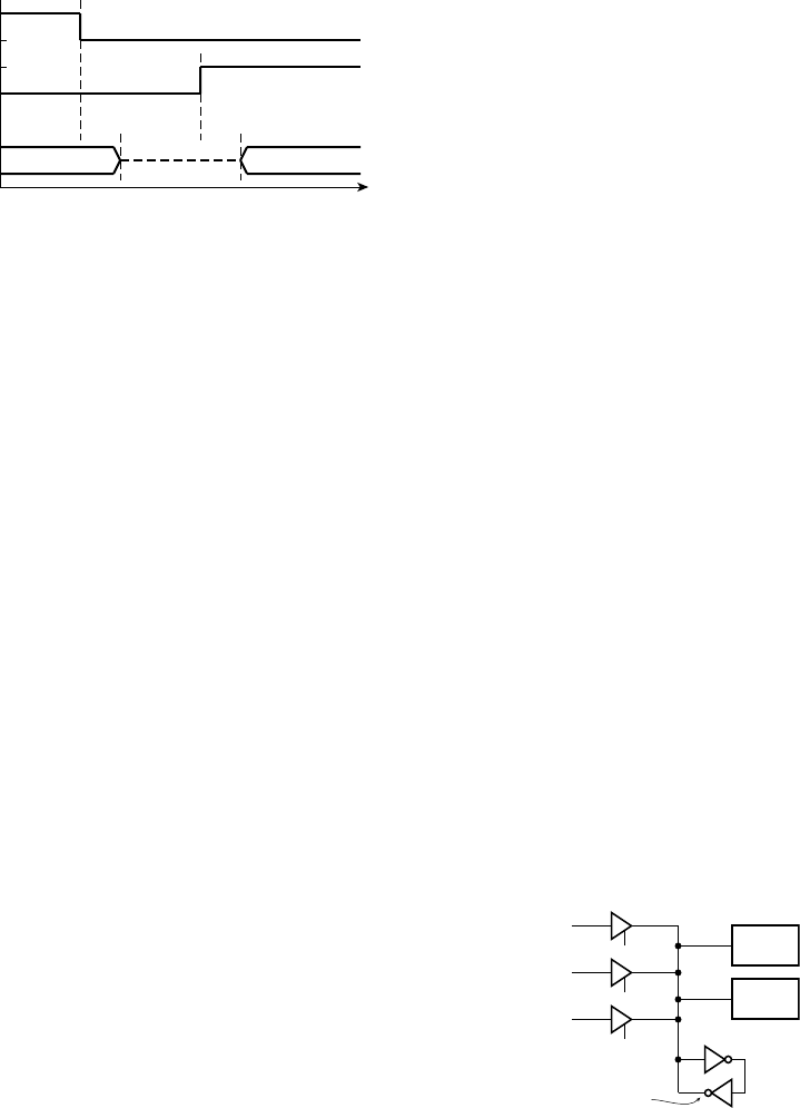
with the capacitance of the drivers and inputs. As a consequence, the wire
delay may be large, making high-speed data transfer difficult. Moreover,
the large capacitance means we need more powerful output-stage circuits,
increasing the area and power consumption of the chip.
A second issue is difficulty in designing the control that selects among
data sources. The control section must ensure that one source’s drivers are
disabled before any other source’s drivers are enabled. When we design
the control section, we need to take into account the timing involved in
disabling and enabling drivers. This is shown in Figure 8.24. When the
enable input of a driver changes to 0, there is a delay, t
off
, before the driver
disconnects from the bus. Similarly, when the enable input changes to 1,
there is a delay, t
on
, before the driver delivers a valid low or high logic
level on the bus. In the intervening time, the bus floats, indicated on the
timing diagram by a dashed line midway between the low and high logic
levels. Since there is no output driving a low or high logic level on the bus
signals, each signal drifts to an unspecified voltage.
Letting the bus float to an unspecified logic level can cause switching
problems in some designs. The bus signal might float to a voltage around the
switching threshold of the bus destination inputs. Small amounts of noise
voltage induced onto the bus wire can cause the inputs to switch state fre-
quently, causing spurious data changes within the data destination and con-
suming power unnecessarily. We can avoid floating logic levels on the bus
signals by attaching a weak keeper to the signal, as shown in Figure 8.25.
The keeper consists of two inverters providing positive feedback to the bus
signal. When the bus is forced to a low or high logic level by a bus driver, the
positive feedback keeps it at that level, even if the forcing driver is disabled.
The transistors in the output circuit of the inverter driving the bus are small,
with relatively high on-state resistance, and so cannot source or sink much
current. They are easily overridden by the output stages of the bus drivers.
When we need to change from one data source to another, it might
seem reasonable to disable one driver at the same time as enabling the
next driver. However, this can cause driver contention. If the t
off
delay of
the disabled driver is at the maximum end of its range and the t
on
delay of
the enabled driver is at the minimum end, there will be a period of overlap
en2
en1
bus
t
off
data 1 data 2
t
on
FIGURE 8.24 Tristate disable
and enable timing.
weak
drive
FIGURE 8.25 A bus keeper
for maintaining valid logic levels.
8.3 Parallel Buses
CHAPTER EIGHT 343
344 CHAPTER EIGHT i/o interfacing
where some bits of the enabled driver may be driving opposite logic levels to
those of the disabled driver. The overlap will be short-lived and is unlikely
to destroy the circuit. However, it does contribute extra power consump-
tion and heat dissipation and ultimately will reduce the operating life of
the circuit. The overlap effect can be exacerbated by clock skew in the
control section. If the flip-flop that generates the enabling signal receives
its clock earlier than the flip-flop that generates the disabling signal, there
will be an increased chance of overlap, even if the on and off delays of the
tristate drivers are near their nominal values. Given these considerations,
the safest approach when designing control for tristate buses is to include
a margin of dead time between different data sources driving the bus. A
conservative approach is to defer enabling the next driver until the clock
cycle after that in which the previous driver is disabled. A more aggressive
approach is to delay the rising edges of the enable signals, for example,
using the circuit of Figure 8.26, to avoid overlap between drivers. As many
pairs of inverters are included as give the required delay. However, this
approach requires very careful attention to timing analysis to ensure that it
works effectively across the expected range of operating conditions.
A third issue relating to design of tristate buses is the support pro-
vided by CAD tools. Not all physical design tools provide the kinds of
timing and static loading analyses needed to design tristate buses effec-
tively. Similarly, tools that automatically incorporate circuit structures to
enable testing of circuits after their manufacture don’t always deal with
tristate buses correctly. If the tools we use don’t support tristate buses, we
must resort to manual methods to complete and verify our design.
A final issue is that not all implementation fabrics provide tristate
drivers. For example, many FPGA devices do not provide tristate drivers
for internal connections, and only provide them for external connections
with other chips. If we want to design a circuit that can be implemented in
different fabrics with minimal change, it is best to avoid tristate buses.
In summary, tristate buses allow us to trade off significantly reduced
wiring complexity against performance and design complexity, provided
that our chosen implementation fabric allows tristate drivers and our
CAD tool suite supports design and analysis of tristate buses. For designs
that don’t have stringent performance requirements, tristate buses can
be a good choice. In the case of bus connections between chips on a
printed circuit board, tristate buses are usually preferred. For that reason,
fabrics such as FPGAs provide tristate drivers that can be used to drive
output pins.
d_busd
en
FIGURE 8.26 A circuit to
delay the rising edge of a bus
enable signal.

Modeling Tristate Drivers in Verilog
There are two aspects to modeling tristate drivers: representing the high-
impedance state, and representing the enabling and disabling of drivers.
In previous chapters, we have used single-bit Verilog net and variable val-
ues to represent single-bit logic levels. Nets and variables can also take on
the value Z for representing the high-impedance state. In a Verilog model
for a circuit, we can assign Z to an output to represent disabling the
output. Subsequently, assigning 0 or 1 to the output represents enabling
it again.
There are several additional points we should make about modeling
tristate drivers in Verilog. First, we can write a Z value using either an
uppercase or lowercase letter. Thus, 1'bZ and 1'bz are the same. Second,
we can only write literal Z values as part of a binary, octal or hexadecimal
number, such as 1'bZ, 3'oZ and 4'hZ. In an octal number, a Z represents
three high-impedance bits, and in a hexadecimal number, a Z represents
four high-impedance bits. Third, Verilog allows us to use the keyword tri
instead of wire for a net connected to the output of a tristate driver. Thus,
we might write the following declaration in a module:
tri d_out;
or the following port declaration:
module m ( output tri a, ... );
Apart from the use of the different keyword, a tri net behaves exactly
the same as a wire net. The tri keyword simply provides documentation
of our design intent. Note that there is no corresponding keyword for a
variable that is assigned a Z value; we continue to use the reg keyword
for that purpose.
example 8.7 Write a Verilog statement to model a tristate driver for an
output net
d_out. The driver is controlled by a net d_en, and when enabled,
drives the value of an input
d_in onto the output net.
solution We can use an assignment statement, as follows:
assign d_out = d_en ? d_in : 1'bZ;
8.3 Parallel Buses
CHAPTER EIGHT 345
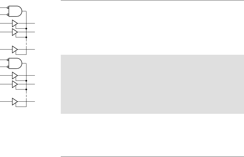
346 CHAPTER EIGHT i/o interfacing
For multibit buses, we can use vectors whose elements include
Z values. While we can assign 0, 1 and Z values individually to elements
of vectors, we usually assign either a vector containing just 0 and 1 values
to represent an enabled driver or a vector of all Z values to represent a
disabled driver. Verilog’s implicit resizing rules for vector values involve
extending with Z elements if the leftmost bit of the value to be extended is
Z. So we can write 8'bz to get an 8-element vector of Z values.
example 8.8 The SN74x16541 component manufactured by Texas
Instruments is a dual 8-bit bus buffer/driver in a package for use in a printed cir-
cuit board system. The internal circuit of the component is shown in Figure 8.27.
Develop a Verilog model of the component.
solution We can use vector ports for each of the 8-bit inputs and out-
puts, and single-bit ports for the enable inputs. The module definition is:
module sn74x16541 ( output tri [7:0] y1, y2,
input [7:0] a1, a2,
input en1_1, en1_2, en2_1, en2_2 );
assign y1 = (~en1_1 & ~en1_2) ? a1 : 8'bz;
assign y2 = (~en2_1 & ~en2_2) ? a2 : 8'bz;
endmodule
Each assignment within the module represents one of the 8-bit sections of the
component. The condition in the assignment determines whether the 8-bit
tristate driver is enabled or disabled. The driver is disabled by assigning a vector
value consisting of all Z elements. Note the use of the
tri keyword in the declara-
tion of the output ports to indicate that they can be assigned Z values.
When we have multiple data sources for a tristate bus, our Verilog
model includes multiple assignment statements that assign values to the
bus. Verilog must resolve the values contributed by the separate assign-
ments to determine the final value for the bus. If one assignment con-
tributes 0 or 1 to a bus and all of the others contribute Z, the 0 or 1
value overrides the others and becomes the bus value. This corresponds
to the normal case of one driver being enabled and the rest disabled.
If one assignment contributes 0 and another contributes 1, we have a
conflict. Verilog then uses the special value X, called unknown, as the
final bus value, since it is unknown whether a real circuit would pro-
duce a low, high or invalid logic level on the bus. Depending on how the
Verilog model of a data destination receiving an X value is written, it
might propagate the unknown value to its outputs, or produce arbitrary
y1(0)a1(0)
a1(1)
…
…
…
a1(7)
en1_1
en1_2
y1(1)
y1(7)
y2(0)a2(0)
a2(1)
…
…
…
a2(7)
en2_1
en2_2
y2(1)
y2(7)
FIGURE 8.27 Internal circuit
of the 16541 component.

0 or 1 values. Ideally, it would include a verification test statement that
would detect unknown input values. If all assignments to a bus contribute
Z, the final signal value is Z. This corresponds to the bus floating. Again,
since this does not represent a valid logic level, a Verilog model of a data
destination receiving a Z input should propagate an X output and detect
the error condition.
An important point to realize about the Z and X values is that they do
not represent real logic levels in a physical circuit. Rather, assignment of
Z to an output is a notational device interpreted by synthesis CAD tools
as implying a tristate driver for the output. Assignment of X to an output
is a notational device used in simulation to propagate error conditions in
cases where we cannot determine a valid output value. We can write Ver-
ilog statements that test whether a bus has the value Z or X, but it only
makes sense to do so in testbench models, for example, in an if statement
to verify that all drivers of a bus have been disabled or that there is no bus
conflict. Since, according to our digital abstraction, signals in a physical
circuit are only ever 0 or 1, a real digital component cannot sense any
other level.
If we need to test for Z or X values in a testbench model, we should
use different equality and inequality operators from those we have used
so far. The == operator in Verilog, known as the logical equality operator,
represents a hardware equivalence operation. If either operand is Z or X,
the result is X, since it is unknown whether the values in a real circuit are
equivalent or not. Similarly, the ! = operator, logical inequality, represents
a hardware unequivalence operation, and returns X if either operand is Z
or X. Thus, for example, the expressions 1'b0 = = 1'bX and 1'bZ != 1'b1
both yield X. If we want to test for Z and X values, we must use the
=== and !== operators, known as the case equality and case inequality
operators, respectively. These perform an exact comparison, including X
and Z values. Thus, 1'b0 = = = 1'bX yields 0 (false), and 1'bZ != = = 1'b1
yields 1 (true). Note that, like the Z value, we can use an uppercase or
lowercase letter, and we can only write literal X values in binary, octal, or
hexadecimal numbers.
example 8.9 Suppose a Verilog module includes the following
declarations and assignments
tri [11:0] data_1, data_2, data_bus;
wire sel_1, sel_2;
...
assign data_bus = sel_1 ? data_1 : 12'hz;
assign data_bus = sel_2 ? data_2 : 12'hz;
8.3 Parallel Buses CHAPTER EIGHT 347
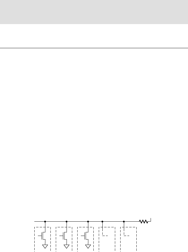
348 CHAPTER EIGHT i/o interfacing
Write a test to verify that the values of all elements of the bus signal are all valid
logic levels, or that all drivers are disabled.
solution Unfortunately, Verilog does not provide an operation expressly
for testing for X or Z values within a vector. However, we can make use of a
property of the reduction XOR operator,
^. This operator can be applied to
a vector to form the XOR of all of the bits of the vector, yielding a single-bit
result. If all of the bits are 0 or 1, the result is 0 or 1, but if any bit is X or Z, the
result is X. Thus, our test can be written as:
if ((^data_bus) = = = 1'bx && data_bus != = 12'hz)
$display("Invalid value on data_bus");
Note that the first part of the condition includes the case of all elements being
Z, so we need to check for that case separately.
8.3.3 OPEN-DRAIN BUSES
A third solution to avoid bus contention is to use open-drain drivers,
as shown in Figure 8.28. Each driver connects the drain terminal of a
transistor to the bus signal. When any of the transistors is turned on, it
pulls the bus signal to a low logic level. When all of the transistors are
turned off, the termination resistor pulls the bus signal up to a high logic
level. If multiple drivers try to drive a low logic level, their transistors
simply share the current load. If there is a conflict, with one or more
drivers trying to drive a low level and others letting the bus be pulled up,
the low-level drivers win. Sometimes, this kind of bus is called a wired-
AND bus, since the bus signal is only 1 if all of the drivers output 1. If
any driver outputs 0, the bus signal goes to 0. The AND function arises
from the wiring together of the transistor drains. We can also use this
form of bus with drivers that use bipolar transistors instead of MOSFET
transistors. In that case, we connect the collector terminal of a transis-
tor to the bus signal, as shown in Figure 8.29. Such a driver is called an
open-collector driver.
+V
FIGURE 8.28 Open-drain
bus structure.
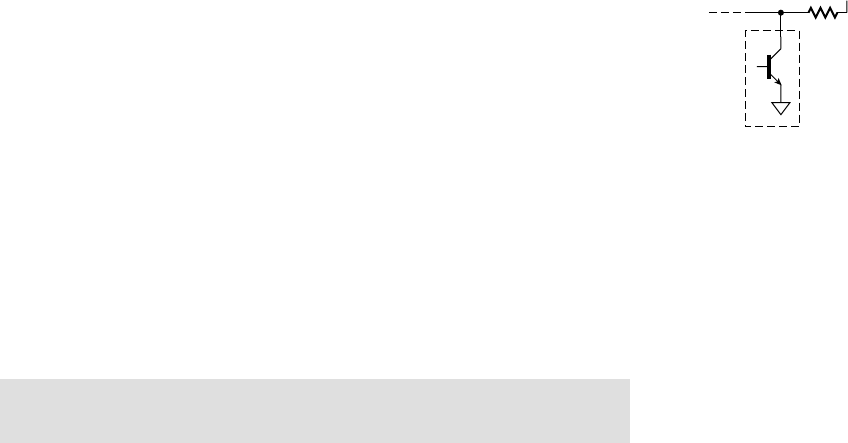
Given the need for a pull-up resistor on each bus signal, open-drain
or open-collector buses are usually found outside integrated circuits.
For example, they may be used for a bus that connects a number of
integrated circuits together, or for the signals in a backplane bus that
connects a number of printed circuit boards together. Implementing
pull-up resistors within an integrated circuit takes up significant area
and consumes power. Hence, we usually use multiplexed or tristate
buses within an integrated circuit chip. If we need the AND function
that would be formed by open-drain connection, we can implement it
with active gates.
Modeling Open-Drain and Open-Collector Connections in Verilog
We can model open-drain and open-collector drivers using a different
kind of net, declared with the keyword wand (short for wired-AND). For
example:
wand bus_sig;
We assign 0 to a wand net to represent a driver whose output transistor
is turned on, pulling the net low. We assign 1 to the net to represent a
driver whose output transistor is turned off. When a wand net is resolved,
any 0 values override all other values. However, if all of the drivers are
turned off, contributing 1 values, the final value of the net is 1. Note that
the pull-up resistor for the bus is not explicitly represented in the model;
rather, it’s effect is implicit in the declaration of the net as wand instead
of wire.
8.3.4 BUS PROTOCOLS
In most design projects, subsystems are often designed by different team
members. Some subsystems may also be procured from external provid-
ers, or be implemented using off-the-shelf components. If the subsystems
are to be interconnected using buses, it would be preferable for them to
use the same bus signals with the same timing requirements; otherwise,
interface glue logic is required. In order to facilitate connection of sepa-
rately designed components, a number of common bus protocols have
been specified. Some of the specifications are embodied in industry and
international standards, whereas others are simply specifications agreed
upon or promoted by component vendors. The specification of a bus pro-
tocol includes a list of the signals that interconnect compliant compo-
nents, and a description of the sequences and timing of values on the
signals to implement various bus operations.
8.3 Parallel Buses CHAPTER EIGHT 349
+V
FIGURE 8.29 Open-collector
bus driver.
350 CHAPTER EIGHT i/o interfacing
Bus specifications and protocols vary, depending on their intended
use. Some, intended for connecting separate chips on a circuit board or
separate boards in a system, use tristate drivers for signals that have mul-
tiple data sources. Examples include the PCI bus used to connect add-on
cards to personal computer systems, and the VXI bus used to connect
measurement instruments to controlling computers. Others are intended
for connecting subsystems within an IC. They have separate input and
output signals, allowing for connection using multiplexers or switching
circuits. Examples include the AMBA buses specified by ARM, the Core-
Connect buses specified by IBM, and the Wishbone bus specified by the
OpenCores Organization. Buses also vary in the number of parallel signals
for transferring addresses and data, and in the speed of operation. Some,
intended for high-speed data transfer, provide for the kinds of techniques
we mention in Chapter 7, such as burst transfers and pipelining.
In this section, we will describe the relatively simple I/O bus protocol
used by the Gumnut core. We have already introduced several aspects of
the bus specification in preceding examples in this chapter. We will draw
all of the aspects of the specification together here.
The Wishbone I/O bus signals for the Gumnut are described in the
Verilog module definition in Example 8.3 and are shown as part of the
Gumnut schematic symbol in Figure 8.21. To summarize, the signals are:
port_cyc_o: a “cycle” control signal that indicates that a sequence of
I/O port operations is in progress.
port_stb_o: a “strobe” control signal that indicates an I/O port
operation is in progress.
port_we_o: a “write enable” control signal that indicates the opera-
tion is an I/O port write.
port_ack_i: a status signal that indicates that the I/O port acknowl-
edges completion of the operation.
port_adr_o: the 8-bit I/O port address.
port_dat_o: The 8-bit data written to the addressed I/O port by an
out instruction.
port_dat_i: the 8-bit data read from the addressed I/O port by an inp
instruction.
When the Gumnut core executes an out instruction, it performs a port
write operation. The timing of the operation is shown in Figure 8.30. Tran-
sitions are synchronized by the system clock. The Gumnut starts a write
operation by driving the port_adr_o signals with the address computed
by the out instruction and the port_dat_o signals with the data from the
source register of the out instruction. It sets the port_cyc_o, port_stb_o
왘
왘
왘
왘
왘
왘
왘
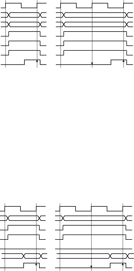
and port_we_o control signals to 1 to indicate commencement of the write
operation. The system in which the Gumnut is embedded decodes the port
address to select an I/O controller and to enable the addressed output reg-
ister to store the data. If the addressed controller is able to update the regis-
ter within the first clock cycle, it sets the port_ack_i signal to 1 in that cycle,
as shown in Figure 8.30(a). On the next rising clock edge, the Gumnut sees
port_ack_i at 1 and completes the operation by driving port_cyc_o, port_
stb_o
and port_we_o back to 0. If, on the other hand, the addressed con-
troller is slow and is not able to update the output register within the cycle,
it leaves port_ack_i at 0, as shown in Figure 8.30(b). The Gumnut sees
port_ack_i at 0 on the rising clock edge, and extends the operation for a
further cycle. The controller can keep port_ack_i at 0 for as long as it needs
to update the register. Eventually, when it is ready, it drives port_ack_i to 1
to complete the operation. This form of synchronization, involving strobe
and acknowledgment signals, is often called handshaking.
The Gumnut performs a port read operation when it executes an inp
instruction. The timing for the operation, shown in Figure 8.31, is similar
clk
port_adr_o
port_cyc_o
port_dat_o
port_ack_i
port_stb_o
port_we_o
(a) (b)
FIGURE 8.30 Timing for
Gumnut I/O write operations:
without wait cycles (a), and with
one wait cycle (b).
8.3 Parallel Buses CHAPTER EIGHT 351
clk
port_adr_o
port_cyc_o
port_dat_i
port_ack_i
port_stb_o
port_we_o
(a) (b)
FIGURE 8.31 Timing for
Gumnut I/O read operations:
without wait cycles (a), and with
one wait cycle (b).
352 CHAPTER EIGHT i/o interfacing
to that for a port write. The Gumnut starts the port read operation by
driving the port_adr_o signals with the computed address, driving the
port_cyc_o and port_stb_o signals to 1, and leaving port_we_o at 0.
Again, the system decodes the address to select an I/O controller and
enable the addressed input register onto the port_dat_i signals. The con-
troller drives the port_ack_i signal to 1 as soon as it has supplied the data,
either during the first cycle, as in Figure 8.31(a), or in a subsequent cycle,
as in Figure 8.31(b). On seeing port_ack_i at 1, the Gumnut transfers the
data from the port_dat_i signals to the destination register identified in
the inp instruction. It then completes the port read operation by driving
port_cyc_o and port_stb_o back to 0.
At first sight, it might appear that the port_cyc_o and port_stb_o sig-
nals are duplicates of each other. However, the Wishbone bus specification
defines other more involved operations in which the two control signals
serve distinct purposes. While the Gumnut does not use those operations,
it includes the signals in order to maintain compatibility with the Wish-
bone specification. The additional signal is a small cost to pay for compat-
ibility with a large pool of third-party components.
1. If a system requires connection of multiple data sources and
destinations, why can we not just connect them directly as shown
in Figure 8.18?
2. In a multiplexed bus system, why might it be desirable to subdivide
the multiplexers and distribute them around the chip?
3. How does a tristate bus avoid logic-level contention on bus signals?
4. Why should we avoid fl oating bus signals?
5. What is a weak keeper?
6. What problems can arise if we disable one tristate bus driver at
the same time as enabling the next driver? How can we avoid the
problems?
7. Write a Verilog assignment that represents a tri-state bus driver for
an 8-bit bus.
8. What value results on a Verilog wire net when two tristate drivers
are enabled and driving opposite logic levels?
9. Why is a signal connecting several open-drain drivers called a wired-
AND connection?
10. Write a Verilog declaration that represents an open-drain bus.
11. What is a bus protocol?
KNOWLEDGE
TEST QUIZ
KNOWLEDGE
TEST QUIZ

8.4 SERIAL TRANSMISSION
Throughout this book, we have described transfer of binary-encoded data
using parallel transmission, in which we dedicate one signal wire per bit
of encoded data. While this might appear to give us the fastest possible
rate of data transfer, there are some disadvantages. The most obvious is
that we require one signal wire per bit. For wide encodings, the wiring
takes up significant circuit area, and makes layout and routing of the cir-
cuit more complex. For connections that extend between chips, parallel
transmission requires more pad drivers and receivers, more pins, and more
PCB traces. These all add cost to the system. Moreover, there are second-
ary effects, such as increased delay due to the extra space required for the
connections, problems with crosstalk between wires routed in parallel,
and problems with skew between signals. Dealing with these problems
adds cost and complexity to the system. In this section, we will describe
an alternative scheme for transferring binary-encoded data. The scheme
is called serial transmission, since bits are transmitted one bit at a time in
series over a single signal wire.
8.4.1 SERIAL TRANSMISSION TECHNIQUES
In order to transform data between parallel and serial form, we can use
shift registers, introduced in Section 4.1.2. At the transmitting end, we
load the parallel data into a shift register and use the output bit at one
end of the register to drive the signal. We shift the content of the register
one place at a time to drive successive bits of data onto the signal. At
the receiving end, as each bit value arrives on the signal, we shift it into
a shift register. When all the bits have arrived, the complete data code
word is available in parallel form in the shift register. We sometimes use
the term serializer/deserializer, or serdes, for shift registers used in this
way. The advantage of serial transmission is that we only need one signal
wire to transfer the data. Thus, we reduce the circuit area and cost for
the connection. Moreover, if necessary, we can afford to optimize the
signal path so that bits can be transferred at a very high rate. Some serial
transmission standards in use today allow for rates exceeding 10 gigabits
per second.
example 8.10
Show how a 64-bit data word can be transmitted serially
between two parts of a system. Assume that the transmitter and the receiver
are both within the same clock domain, and that the signal
start is set to 1 on a
clock cycle in which data is ready to be transmitted.
solution At the transmitting end, we need a 64-bit shift register with
parallel load control and an output from the least signifi cant bit. At the receiv-
ing end, we also need a 64-bit shift register, but with a single-bit input and
8.4 Serial Transmission CHAPTER EIGHT 353
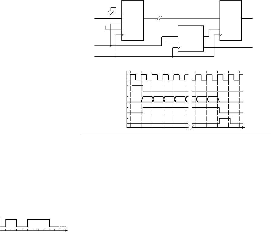
354 CHAPTER EIGHT i/o interfacing
One important issue that we need to address when transferring data
serially is the order in which we transmit the bits. In principle, the order
is arbitrary, so long as the transmitter and receiver agree. Otherwise, the
receiver will end up with the bits in reverse order. In Example 8.10, we
transmit the least significant bit first, and so shift bits into the receiver shift
register at the most significant end, shifting them down to the least signifi-
cant end. Fortunately, serial transmission in a system is often governed by
a standard that specifies the order. This absolves us of the need to decide.
Another important issue is synchronization of the transmitter and the
receiver. If we just drive the signal with the data bit values, there is no
indication of when the time for one bit ends and the time for the next
bit starts. This form of serial transmission is called non-return to zero
(NRZ), and is illustrated in Figure 8.34, which shows the logic levels on
a signal for NRZ serial transmission of the value 11001111, with the
most significant bit being transmitted first. We assume in this case that
the value on the signal when no bit is being transmitted is 0. In the figure,
parallel data output. The connections are shown in Figure 8.32. The fi gure also
shows the control section that sequences the serial transmission. When a
start
pulse occurs, the control section activates the receiver clock enable,
rx_ce, for
64 cycles to shift the serial data in. The control section then pulses
rx_rdy to
indicate that the received data is ready. A timing diagram for one transmission is
shown in Figure 8.33. We can implement the control logic with a counter and a
simple fi nite-state machine.
64-bit
shift reg
D_in
D
CE
load_en
Q0
64-bit
shift reg
D_in
CE
Q
start
reset
tx_D
serial_D
rx_D
rx_rdy
clk
start
reset
rx_ce
rx_rdy
receiver
control
+V
clk clk
clk
FIGURE 8.32 Serial
transmission of 64-bit data within
a clock domain.
rx_rdy
rx_ce
serial_D
start
clk
D0 D1 D62 D63D2 D3
FIGURE 8.33 Timing
diagram for the serial receiver
control.
FIGURE 8.34 Serial
transmission of the value
11001111.
we have drawn a timescale showing the interval in which each bit occurs.
However, that information is implicit, rather than being explicitly trans-
mitted to the receiver along with the data. If the receiver, for some reason,
assumed intervals twice as long for each bit, it would receive the value
10110000. To avoid this problem, we need to synchronize the transmitter
and receiver, so that the receiver samples each bit value on the signal at
some time during the interval when the transmitter drives the signal with
the bit value.
There are three basic ways in which we can synchronize the transmit-
ter and receiver. The first is by transmitting a clock on a separate signal
wire. We saw this scheme in Example 8.10. The second is by signaling
the start of a serial code word and relying on the receiver to keep track
of the individual bit intervals. A common way of doing this originated
with teletypes, which were computer terminals consisting of a keyboard
and a printer connected to a remote computer using serial transmission.
A refined version of such serial transmission is still used to connect some
devices to serial communications ports on modern PCs.
In this second scheme, the signal is held at a high logic level when
there is no data to transmit. When data is ready to be transmitted, trans-
mission proceeds as shown in Figure 8.35, again with the most significant
bit transmitted first. The signal is brought to a low logic level for one bit
time to indicate the start of transmission. We call this the start bit. After
that, the bits of data are transmitted, each for one bit time. We might also
transmit a parity bit after the data bits, in case the signal wire is subject
to induced noise, though this is not shown in the figure. This would allow
us to detect some errors that might occur during transmission. Finally,
we drive the signal high for one further bit time to indicate the end of
transmission of the data. We call this the stop bit. We can then transmit
the next piece of data, starting with a start bit, or leave the signal high if
there is no data ready to transmit.
At the receiving end, the receiver monitors the logic level on the
signal. While it remains at a high logic level, the receiver is idle. When
the receiver detects a low logic level of the start bit, it prepares to receive
the data. It waits until the middle of the first bit time and shifts the value
on the signal into the receiving shift register. It then waits for further suc-
cessive bit times, shifting each bit into the shift register. The complete data
is available after the last bit is received. The receiver uses the stop-bit time
to return to the idle state.
Note that the transmitter and the receiver must agree on the duration
of the bit times on the signal. Usually, this is fixed in advance, either dur-
ing manufacture or by programming. The transmitter and receiver typi-
cally have independent clocks, each several times faster than the serial bit
rate. The sender uses its clock to transmit the data, and the receiver uses
its clock to determine when to sense the data, synchronized by occurrence
FIGURE 8.35 Serial
transmission of the value
11100100 with start and
stop bits.
8.4 Serial Transmission
CHAPTER EIGHT 355

356 CHAPTER EIGHT i/o interfacing
of the start bit. This is illustrated in Figure 8.36, in which the transmit
clock and receive clock have slightly different frequencies and are not
related in phase. Provided the difference is not too extreme, the drift
from the nominal sampling time does not affect correct reception of the
transmitted data.
Historically, computer component manufacturers provided a compo-
nent called a universal asynchronous receiver/transmitter, or UART, for
serial communications ports. The software on the computer could pro-
gram the bit rate and other parameters. UARTs are still useful in some
applications for connecting remote devices to digital systems via serial
communications links. For example, an instrumentation system with
remote sensors that transmit data at relatively low bit rates can use serial
transmission managed by UARTs.
The third scheme for synchronizing a serial transmitter and receiver
involves combining a clock with the data on the same signal wire. This
avoids the need for tight clock synchronization, since there is an indica-
tion of when each bit arrives. As an example of such a scheme, we will
describe Manchester encoding. As with NRZ transmission, Manchester
encoding transmits each bit of data in a given interval. However, rather
than representing each bit using one or other logic level, it represents a 0
with a transition from low to high in the middle of the bit interval, and a
1 with a transition from high to low. (We could equally well choose the
opposite assignment of transmissions, so long as transmitter and receiver
agree.) At the beginning of the bit interval, a transition may be necessary
to set the signal to the right logic level for the transition in the middle of
the interval. Manchester encoding of the value 11100100 is shown in
Figure 8.37, with the most significant bit transmitted first and with bit
intervals defined by the transmitter’s clock.
Since Manchester encoding of data is synchronized with the trans-
mitter’s clock and that clock is combined with the data, the receiver must
be able to recover the transmitted clock and data from the signal. It does
so using a circuit called a phase-locked loop (PLL), which is an oscillator
whose phase can be adjusted to line up with a reference clock signal. A sys-
tem using Manchester encoding usually transmits a continuous sequence
of encoded 1 bits before transmitting one or more data words. The encod-
ing of such a sequence gives a signal that matches the transmitter’s clock.
Tx_clk
Tx_D
Rx_clk
FIGURE 8.36 Generation
and sampling of serial data using
transmitter and receiver clocks.
FIGURE 8.37 Manchester
encoding of the value 11100100.
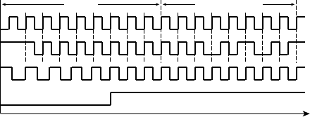
The receiver’s PLL locks onto the signal to give a clock that can be used
to determine the bit intervals for the transmitted data. This is shown in
Figure 8.38.
The main advantage of Manchester encoding over NRZ transmission
is that it contains sufficient transitions to allow clock synchronization with-
out the need for separate signal wires. The disadvantage is that the band-
width of the transmission is double that of NRZ transmission. However,
for many applications, that is not an overriding disadvantage. Manchester
encoding has been used in numerous serial transmission standards, includ-
ing the original Ethernet standard. Other serial encoding schemes that are
similar in concept but more involved are now becoming widely used.
8.4.2
SERIAL INTERFACE STANDARDS
Given the advantages of serial transmission over parallel transmission
for applications where distance and cost are significant considerations,
numerous standards have been developed. These standards cover two
broad areas of serial interfaces: connection of I/O devices to computers,
and connection of computers together to form a network. Since most
digital systems contain embedded computers, they can include standard
interfaces for connecting components. The benefits of doing so include
avoiding the need to design the connection from scratch, and being able
to use off-the-shelf devices that adhere to standards. As a consequence, we
can reduce the cost of developing and building systems, as well reducing
the risk of designs not meeting requirements.
Some examples of serial interface standards for connecting I/O devices
include:
RS-232: This standard was originally defined in the 1960s for
connecting teletype computer terminals with modems, devices
for serial communication with remote computers via phone lines.
Sub sequently, the standard was adopted for direct connection of
terminals to computers. Since most computers included RS232 con-
nection ports, RS232 connections were incorporated in I/O devices
왘
idle data word
Tx_clk
Tx_D
Rx_clk
locked
FIGURE 8.38 Synchronization
of transmit and receive clocks by
a PLL .
8.4 Serial Transmission
CHAPTER EIGHT 357
358 CHAPTER EIGHT i/o interfacing
other than terminals as a convenient way to connect to computers.
Examples included user-interface devices such as mice, and various
measurement devices. Serial transmission in RS232 interfaces uses
NRZ encoding with start and stop bits for synchronization. Data
is usually transmitted with the least significant bit first and most
significant bit last. While RS232 interfaces have now largely been
supplanted by more recent standards, they are still used in some
equipment, for example, bar code readers in point-of-sale terminals,
and industrial measurement devices.
I
2
C: The Inter-Integrated Circuit bus specification is defined by
Philips Semiconductors, and is widely adopted. It specifies a serial
bus protocol for low-bandwidth transmission between chips in a sys-
tem (10kbit/sec to 3.4Mbit/sec, depending on the mode of operation).
It requires two signals, one for NRZ-coded serial data and the other
for a clock. The signals are driven by open-drain drivers, allowing
any of the chips connected to the bus to take charge by driving the
clock and data signals. The specification defines particular sequences
of logic levels to be driven on the signals to arbitrate to see which
device takes charge and to perform various bus operations. The
advantage of the I
2
C bus is its simplicity and low implementation
cost in applications that do not have high performance requirements.
It is used in many off-the-shelf consumer and industrial control chips
as the means for an embedded microcontroller to control opera-
tion of the chip. Philips Semiconductor has also developed a related
bus specification, I
2
S, or Inter-IC Sound, for serial transmission of
digitally encoded audio signals between chips, for example, within a
CD player.
USB: The Universal Serial Bus is specified by the USB Implement-
ers Forum, Inc., a nonprofit consortium of companies founded by
the original developers of the bus specification. USB has become
commonplace for connecting I/O devices to computers. It uses
differential signaling (see Section 6.4.1) on a pair of wires, with a
modified form of NRZ encoding. Different configurations support
serial transfer at 1.5Mbit/sec, 12Mbit/sec or 480Mbit/sec. The USB
specification defines a rich set of features for devices to communicate
with host controllers. Since there is such a diversity of devices with
USB interfaces, application-specific digital systems can benefit from
inclusion of a USB host controller to enable connection of off-the-
shelf devices. USB interface designs for inclusion in ASIC and FPGA
designs are available in component libraries from vendors.
FireWire: This is another high-speed bus defined by IEEE Standard
1394. Whereas USB was originally developed for lower bandwidth
devices and subsequently revised to provide higher bandwidth,
왘
왘
왘
FireWire started out as a high-speed (400Mbit/sec) bus. There is also
a revision of the standard defining transfer at rates up to 3.2Gbit/sec.
FireWire connections use two differential signaling pairs, one for
data and the other for synchronization. As with USB, there is a rich
set of bus operations that can be performed to transmit information
among devices on the bus. FireWire assumes that any device con-
nected to the bus can take charge of operation, whereas USB requires
a single host controller. Thus, there are some differences in the
operations provided by FireWire and USB, and some differences in
the applications for which they are suitable. FireWire has been most
successful in applications requiring high-speed transfer of bulk data,
for example, digital video streams from cameras.
example 8.11 Design an interface to connect an embedded Gumnut core
to a remote temperature sensor. The temperature sensor is an Analog Devices
AD7414 with an I
2
C connection and an alert output that can be connected to a
warning indicator.
solution The OpenCores repository (see Section 8.7, Further Reading)
contains an I
2
C controller component that is Wishbone compliant. We can
use it rather than designing a new I
2
C controller from scratch. We connect
the controller to the Gumnut core’s Wishbone I/O bus, and provide pad
connections to an external I
2
C bus for connecting the temperature sensor. We
connect the alert output of the sensor to an LED indicator. The sensor allows
the embedded software to program threshold temperatures, beyond which the
alert indicator is activated. The system design is shown in Figure 8.39. The use
8.4 Serial Transmission CHAPTER EIGHT 359
wb_adr_i
wb_dat_i
wb_dat_o
wb_rst_i
arst_i
wb_we_i
i2c_master_top
wb_stb_i
wb_cyc_i
wb_ack_o
wb_inta_o
scl_pad_i
scl_pad_o
scl_padoen_o
sda_pad_i
sda_pad_o
sda_padoen_orst_i
Gumnut
port_adr_o
port_dat_o
port_dat_i
port_we_o
port_stb_o
port_cyc_o
port_ack_i
int_req
int_ack
scl
AD7414
sda alert
rst
clk
+V
+V
wb_clk_iclk_i
FIGURE 8.39 A temperature
sensing system using an I
2
C serial
bus.
of the serial I
2
C bus allows connection to the temperature sensor with only
two wires, resulting in a substantial reduction in system cost compared to
connection using a parallel bus.
360 CHAPTER EIGHT i/o interfacing
1. What advantages does serial transmission of data have over parallel
transmission?
2. How do we convert between parallel and serial form for serial data
transmission or reception?
3. What determines the order in which we transmit bits of data?
4. What is meant by non-return to zero (NRZ) transmission?
5. What is the purpose of a start bit and a stop bit in serial
transmission?
6. How does Manchester encoding represent 0 and 1 bits?
7. Why would we adopt a standard serial interface specifi cation rather
than developing a custom interface?
8. Which of I
2
C or FireWire would be most appropriate for connecting
a motor controller and a digital video camera, respectively, to an
embedded system?
8.5 I/O SOFTWARE
Now that we have described the hardware aspects of input and output,
we turn our attention to the corresponding embedded software. We have
seen that an out instruction in the Gumnut core invokes a port write
operation to update an output register in an I/O controller, and an inp
instruction invokes a port read operation to get the value from an input
register. The embedded software running on the core needs to use out and
inp instructions as part of the task of managing input and output devices
to implement the functionality required of the system.
Since I/O devices interact with the real physical world, the embed-
ded software needs to be able to respond to events when they occur, or
to cause events at the right time. Dealing with real time behavior is one
of the main differences between embedded software and programs for
general purpose computers. Embedded software needs to be able to detect
when events occur so that it can react. It also needs to be able to keep
track of time so that it can perform actions at specific times or at regular
intervals. In this section, we will introduce the basic mechanisms for syn-
chronizing embedded software with I/O events.
8.5.1 POLLING
The simplest I/O synchronization mechanism is called polling. It involves
the software repeatedly checking a status input from a controller to see if
an event has occurred. If it has, the software performs the necessary task
to react to the event. If there are multiple controllers, or multiple events to
KNOWLEDGE
TEST QUIZ
KNOWLEDGE
TEST QUIZ

which the software must respond, the software checks each of the status
inputs in turn, reacting to events as they occur, as part of a busy loop.
example 8.12 A factory automation system includes a safety monitoring
subsystem based on an embedded Gumnut core. The core has alarm inputs
from a number of machines that indicate various abnormal operating condi-
tions. These are connected through a controller that has two input registers at
addresses 16 and 17. Each bit of each register represents one alarm input, with
the bit being 0 for normal operation and 1 for an alarm condition. The core also
has a temperature sensor connected to an ADC. The converted value is available
in an input register at address 20, represented as an 8-bit unsigned integer in °C.
A temperature above 50°C is abnormal. The core has an output register at
address 40. Writing a 1 to the least signifi cant bit of the output register activates
an alarm bell, and writing 0 deactivates it. Develop a poll
ing loop for the
embedded software to monitor the inputs and activate the alarm bell when any
abnormal condition arises.
solution The polling loop must repeatedly read the input registers. If any
alarm input bit is 1, or if the temperature value is greater than 50°C, the alarm
bell output bit must be set to 1; otherwise, it must be cleared to 0. The code is
alarm_in_1: equ 16 ; address of alarm_in_1 input register
alarm_in_2: equ 17 ; address of alarm_in_2 input register
temp_in: equ 20 ; address of temp_in input register
alarm_out: equ 40 ; address of alarm_out output register
max_temp: equ 50 ; maximum permissible temperature
poll_loop: inp r1, alarm_in_1
sub r0, r1, 0
bnz set_alarm ; one or more alarm_in_1 bits set
inp r1, alarm_in_2
sub r0, r1, 0
bnz set_alarm ; one or more alarm_in_2 bits set
inp r1, temp_in
sub r0, r1, max_temp
bnc set_alarm ; temp_in > max_temp
out r0, alarm_out ; clear alarm_out
jmp poll_loop
set_alarm: add r1, r0, 1
out r1, alarm_out ; set alarm_out bit 1 to 1
jmp poll_loop
Polling has the advantage that it is very simple to implement, and
requires no additional circuitry beyond the input and output registers
of the I/O controllers. However, it requires that the processor core be
8.5 I/O Software CHAPTER EIGHT 361
362 CHAPTER EIGHT i/o interfacing
continually active, consuming power even when there is no event to react
to. It also prevents the processor from reacting immediately to one event if
it is busy dealing with another event. For these reasons, polling is usually
only used in very simple control applications where there is no need for
fast reaction times.
8.5.2 INTERRUPTS
Probably the most common way to synchronize embedded software with
I/O events is through use of interrupts. The processor executes some back-
ground tasks, and when an event occurs, the I/O controller that detects
the event interrupts the processor. The processor then stops what it was
doing, saving the program counter so that it can resume later, and starts
executing an interrupt handler, or interrupt service routine, to respond to
the event. When it has completed the handler, it restores the saved pro-
gram counter and resumes the interrupted program. In some systems, if
there is no background task to run, the processor may enter a low-power
standby state from which it emerges in response to an interrupt. This has
the benefit of avoiding power consumption due to busy-waiting, though
it may add delay to the interrupt response time if the processor requires
some time to resume full-power operation.
Different processors provide different mechanisms for I/O controllers
to request an interrupt. Some provide very simple mechanisms, such as
that of the Gumnut core that we will describe shortly. Others provide more
elaborate mechanisms, for example, allowing different controllers to be
assigned different priorities, so that a higher-priority event can interrupt
service of a lower-priority event, but not vice versa. Some provide a way for
the controller to select the interrupt handler to be executed by the proces-
sor. However, there are some aspects that are common to most systems.
First, the processor must have an input signal to which controllers can
connect to request interrupts. For older microprocessors and microcon-
trollers, the interrupt request signal is often an active-low signal pulled up
with an external resistor. Each controller connects to the signal with an
open-drain or open-collector driver, pulling the signal low to request an
interrupt. Thus, the signal value is a wired-OR function of the individual
controllers’ requests. For processor cores that are designed to connect to
on-chip I/O controllers, the interrupt request input is typically driven by
active gates forming the OR of the controllers’ requests.
Second, the processor must be able to prevent interruption while it is
executing certain sequences of instructions, often called critical regions.
Examples are instructions that update information shared between an
interrupt handler and other parts of the embedded software. If the proces-
sor is part way through updating such information and is interrupted, the
interrupt handler will see the partially updated information, which may not
correctly represent a valid value. So processors generally have instructions
or other means of disabling interrupts and enabling interrupts.
Third, the processor must be able to save sufficient information about
the program it was executing when interrupted so that it can resume the
program on completion of the interrupt handler. At the least, this includes
saving the program counter value. Since the processor responds to an
interrupt after completing one instruction and before starting the next,
the program counter contains the address of the next instruction in the
program. That is the instruction to be resumed after the interrupt handler.
The processor must provide a register or some other storage in which to
save the program counter. If there is other state information in the pro-
cessor that might be modified by the interrupt handler, such as condition
code bits, they must also be saved and restored.
Fourth, when the processor responds to an interrupt, it must disable
further interrupts. Since response to an interrupt involves saving the inter-
rupted program’s state in registers, if the interrupt handler is itself inter-
rupted, the saved state would be overwritten. Thus, the handler needs to
prevent interruption, at least during the initial stages of responding to an
interrupt.
Some processors allow the storage containing the saved state infor-
mation to be read by a program. That allows a handler to copy the saved
state into memory. The handler can then re-enable interrupts, allowing
the interrupt handler itself to be interrupted to deal with another event.
We call this nested interrupt handing. The handler must disable interrupts
again when it has completed its operation so that it can restore the saved
state before resuming the interrupted program.
Fifth, the processor must be able to locate the first instruction of the
interrupt handler. The simplest way of doing this is for the handler to start
at a fixed or predetermined address in the instruction memory. Alterna-
tive schemes involve the interrupting controller providing a vector: either
a value used to form the address of the handler, or an index into a table
of addresses in memory.
Finally, the processor needs an instruction for the interrupt handler to
return to the interrupted program. Such a return from interrupt instruc-
tion restores the saved program counter and any other saved state.
The Gumnut processor core has all of these features, with the excep-
tion of nested interrupt handing. It has an input signal, int_req, that con-
trollers can drive to 1 to request an interrupt. It includes two instructions
in its instruction set: disi, for disabling interrupts; and enai, for enabling
interrupts. When the core responds to an interrupt, it saves the program
counter and the values of the Z and C condition codes in special inter-
nal registers, and disables further interrupts. The first instruction of the
interrupt handler is located at address 1 in the instruction memory, so
the processor simply loads that address into the program counter to start
8.5 I/O Software CHAPTER EIGHT 363

364 CHAPTER EIGHT i/o interfacing
executing the handler. Finally, the Gumnut instruction set includes the reti
instruction to return from an interrupt handler. It restores the saved values
to the program counter and the Z and C condition code bits, and re-enables
interrupts. Program execution then resumes from where it left off.
There are also requirements on I/O controllers that make interrupt
requests. When an event occurs, the controller must activate the processor’s
interrupt request signal. However, the processor may not respond imme-
diately. The requesting controller must keep the request signal active, oth-
erwise the request may go unnoticed. Failure to respond to an event may
be a critical error in some systems. Processors typically have a mechanism
to acknowledge an interrupt request, that is, to indicate that the event has
been noticed and that the interrupt handler as been activated. If there are
multiple I/O controllers that can request interrupts, the processor needs to
acknowledge each request individually, so that none are overlooked. Once
a request has been acknowledged, the controller must deactivate the inter-
rupt request signal. Otherwise, multiple responses might occur for the one
event. In some cases, that can be as bad as missing an event.
The Gumnut core provides a simple interrupt acknowledgment mech-
anism. It has an output signal, int_ack, that it drives to 1 for one cycle
when it responds to an interrupt request. If there is only one controller
that can request interrupts in a Gumnut system, the controller can use the
int_ack signal to clear its interrupt request state.
example 8.13 Design an input controller that has 8-bit binary-coded
input from a sensor. The value can be read from an 8-bit input register. The
controller should interrupt the embedded Gumnut core when the input value
changes. The controller is the only interrupt source in the system.
solution The controller contains a register for the input value. Since
we need to detect changes in the value, we also need a register for the previous
value, that is, the value on the previous clock cycle. When the current and previ-
ous values change, we set an interrupt-request state bit. Since there is only one
interrupt source, we can use the
int_ack signal from the processor core to clear
the state bit. The controller circuit is shown in Figure 8.40.
example 8.14 Develop a Verilog model of the input controller of
Example 8.13.
solution The module definition includes ports for the I/O bus, plus the
interrupt request and acknowledge connections:
module sensor_controller ( input clk_i, rst_i,
input cyc_i, stb_i,
output ack_o,
(continued)
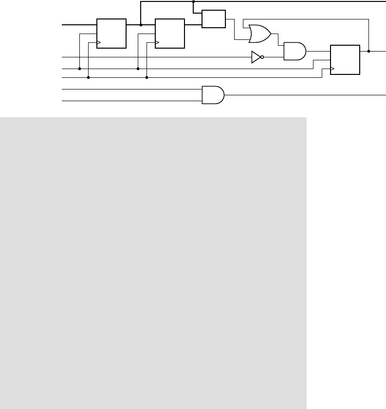
D
reset
QD
reset
Q
D
reset
Q
≠
dat_o
int_req
ack_o
clk_i
rst_i
int_ack
cyc_i
stb_i
sensor_in
clk clk
clk
FIGURE 8.40 Circuit for
an input controller with interrupt
request logic.
8.5 I/O Software
CHAPTER EIGHT 365
output reg [7:0] dat_o,
output reg int_req,
input int_ack,
input [7:0] sensor_in );
reg [7:0] prev_data;
always @(posedge clk_i) // Data registers
if (rst_i) begin
prev_data <= 8'b0;
dat_o <= 8'b0;
end
else begin
prev_data <= dat_o;
dat_o <= sensor_in;
end
always @(posedge clk_i) // Interrupt state
if (rst_i) int_req <= 1'b0;
else
case (int_req)
1'b0: if (dat_o ! = prev_data) int_req <= 1'b1;
1'b1: if (int_ack) int_req <= 1'b0;
endcase
assign ack_o = cyc_i & stb_i;
endmodule
The first always block represents the two data registers, one for the current sen-
sor data value and one for the previous value. The second always block repre-
sents the interrupt request and acknowledge logic. It is essentially a small finite
state machine, with int_req encoding the state. In the state where int_req is 0,
there is no interrupt request. However, if the current value changes from the pre-
vious value, int_req is set to 1. The value of this output is used as the interrupt
request signal to the processor. It stays 1, even when the current value and the
previous value no longer differ. Eventually, when the processor responds to the
interrupt and sets int_ack to 1, int_req is cleared back to 0.

366 CHAPTER EIGHT i/o interfacing
example 8.15 Show the Gumnut assembler code for the interrupt handler
for the sensor controller interrupt. Assume the data register is read at port
address 0.
solution The interrupt handler is
data
saved_r1: bss 1
text
sensor_data: equ 0 ; address of sensor data
; input register
org 1
stm r1, saved_r1
inp r1, sensor_data
... ; process the data
ldm r1, saved_r1
reti
Since the handler needs to use processor register r1, it must save whatever value
is in there from the interrupted program. The data memory location
saved_r1 is
reserved for that purpose. The interrupt handler must be located at address 1 in
the instruction memory. We use an
org directive to ensure this. The instructions
in the handler first save the contents of r1, then read the new value from the con-
troller’s input register. The handler then executes instructions that deal with the
data. Finally, the handler restores the saved value to r1 and uses a
reti instruction
to resume the interrupted program.
If, in a Gumnut-based system, there are several controllers that can
request an interrupt, the interrupt handler must be able to determine
which controller requested an interrupt so that it can execute the appro-
priate response. In such a system, each controller must provide status
information in a status register that indicates whether it has requested an
interrupt. Furthermore, the int_ack signal is not sufficient to distinguish
which request is acknowledged. Instead, the processor must perform some
other action to acknowledge the interrupt. We could acknowledge and
clear a controller’s interrupt request as a side-effect of its status register
being read. Alternatively, we could require a write operation to a control
register to acknowledge the request.
8.5.3 TIMERS
As we mentioned earlier, many real-time embedded systems must perform
actions at specific times or at periodic intervals. For these systems, we
need to include some form of timer. We showed in Chapter 4 that we can

use a counter to derive a periodic signal from the system clock. We can
use such a signal as a time base: each cycle represents one unit of time in
the embedded system. We also showed how we can use a loadable down
counter as an interval timer. A common use for interval timers in real-time
embedded systems is to generate an interrupt for the processor at some
programmable multiple of a time base. The interval timer acts as an I/O
controller, often called a real-time clock, with an output register for pro-
gramming the time interval. The interrupt handler for the timer can then
perform any required periodic actions.
example 8.16 Develop a Verilog model for a real-time clock controller
for the Gumnut processor. The controller has a 10µs time base derived from
a 50MHz system clock, and an 8-bit output register for the value to load into
the counter. A write operation to the output register causes the counter to be
loaded. After the counter reaches 0, it reloads the value from the output register
and requests an interrupt. The controller has an input register for reading the
current count value. The counter also has a 1-bit control output register. When
bit 0 of the register is 0, interrupts from the controller are masked, and when it
is 1, they are enabled. The counter has a status register, in which bit 0 is 1 when
the counter has reached 0 and been reloaded, or 0 otherwise. Other bits of the
register are read as 0. Reading the register has the side effect of acknowledging a
requested interrupt and clearing bit 0. The counter output and input registers are
located at the base port address, and the control and status registers are at offset
1 from the base port address.
solution The module definition for the controller has ports for the I/O
bus, and uses the
stb_i port for the decoded base port address:
module real_time_clock ( input clk_i, // 50 MHz clock
input rst_i,
input cyc_i, stb_i, we_i,
output ack_o,
input adr_i,
input [7:0] dat_i,
output [7:0] dat_o,
output int_req );
parameter clk_freq = 50000000;
parameter timebase_freq = 100000;
parameter timebase_divisor = clk_freq / timebase_freq;
reg [7:0] count_value;
reg trigger_interrupt;
reg int_enabled, int_triggered;
8.5 I/O Software
CHAPTER EIGHT 367
(continued)

368 CHAPTER EIGHT i/o interfacing
integer timebase_count;
reg [7:0] count_start_value;
always @(posedge clk_i) // Counter
if (rst_i) begin
timebase_count <= 0;
count_start_value <= 8'b0;
count_value <= 8'b0;
trigger_interrupt <= 1'b0;
end
else if (cyc_i && stb_i && !adr_i && we_i) begin
timebase_count <= 0;
count_start_value <= dat_i;
count_value <= dat_i;
trigger_interrupt <= 1'b0;
end
else if (timebase_count = = timebase_divisor – 1) begin
timebase_count <= 0;
if (count_value == 8'b00000000) begin
count_value <= count_start_value;
trigger_interrupt <= 1'b1;
end else begin
count_value <= count_value — 1;
trigger_interrupt <= 1'b0;
end
end
else begin
timebase_count <= timebase_count + 1;
trigger_interrupt <= 1'b0;
end
always @(posedge clk_i) // Control register
if (rst_i)
int_enabled <= 1'b0;
else if (cyc_i && stb_i && adr_i && we_i)
int_enabled <= dat_i[0];
always @(posedge clk_i) // Interrupt register
if (rst_i || (cyc_i && stb_i && adr_i && !we_i))
int_triggered <= 1'b0;
else if (trigger_interrupt)
int_triggered <= 1'b1;
assign dat_o = !adr_i ? count_value : {7'b0, int_triggered};
assign int_req = int_triggered & int_enabled;
assign ack_o = cyc_i & stb_i;
endmodule

The first always block represents the time-base divider, interval counter and
counter output register. The variable
timebase_count is used to divide the
50MHz clock to derive the 100kHz time base, and the variable
count_start_
value stores the value for the counter output register. The count value is repre-
sented by the variable
count_value. The variable trigger_interrupt is an internal
control variable used to manage interrupt requests. On reset, the variables are
cleared to zeros. When a port write operation is performed with the least signifi-
cant address bit being 0, the written data is used to update
count_start_value,
and the counters are cleared to zeros again. On other clock cycles, the counters
are incremented. When the time base counter reaches its terminal count, it wraps
to zero, and
count_value is decremented. When count_value reaches zero, it is
reloaded from
count_start_value, and the trigger_interrupt variable is set to 1.
The second always block represents the control register, containing the interrupt-
enable bit. On reset, the bit is cleared to 0. Otherwise, when a write operation is
performed with the least significant address bit being 1, the bit is updated with
the written port data.
The third always block represents the one-bit state register that determines when
an interrupt event has occurred. The variable
int_triggered is set to 1 when the
trigger_interrupt variable is 1, that is, when count_value is reloaded after having
reached zero. The variable is cleared to 0 on reset, and also on a port read opera-
tion that reads the status register.
The remaining assignments implement the rest of the required functionality. The
assignment to
dat_o selects the value provided for a port read operation: either
the count value or the interrupt status bit. The assignment to
int_req causes an
interrupt request when the triggering event has occurred and interrupt requests
are enabled. The assignment to
ack_o implements the controller’s response to bus
operations, indicating that the controller is ready without delay.
example 8.17 Suppose a Gumnut system includes the real-time clock
controller of Example 8.16 with the registers located at base port address 16.
Develop Gumnut code that calls the subroutine
task_2ms every 2ms. In between
activations, the program stands by in low-power mode. The subroutine should
not be called as part of the interrupt handler, since other interrupts should be
permitted during execution of the subroutine.
solution The code is
;;; --------------------------------------------------------
;;; Program reset: jump to main program
text
org 0
jmp main
8.5 I/O Software
CHAPTER EIGHT 369
(continued)

370 CHAPTER EIGHT i/o interfacing
;;; --------------------------------------------------------
;;; Port addresses
rtc_start_count: equ 16 ; data output register
rtc_count_value: equ 16 ; data input register
rtc_int_enable: equ 17 ; control output register
rtc_int_status: equ 17 ; status input register
;;; ---------------------------------------------------------
;;; Interrupt handler
data
int_r1: bss 1 ; save location for
; handler registers
text
org 1
int_handler: stm r1, int_r1 ; save registers
check_rtc: inp r1, rtc_status ; check for
; RTC interrupt
sub r0, r1, 0
bz check_next
add r1, r0, 1
stm r1, rtc_int_flag ; tell main
; program
check_next: ...
int_end: ldm r1, int_r1 ; restore registers
reti
;;; --------------------------------------------------------
;;; init_interrupts: Initialize 2ms periodic interrupt, etc.
data
rtc_divisor: equ 199 ; divide 100 kHz down
; to 500 Hz
rtc_int_flag: bss 1
text
init_interrupts: add r1, r0, rtc_divisor
out r1, rtc_start_count
add r1, r0, 1
out r1, rtc_int_enable
stm r0, rtc_int_flag
... ; other initializations
ret
;;; ---------------------------------------------------------
(continued)

;;; main program
text
main: jsb init_interrupts
enai
main_loop: stby
ldm r1, rtc_int_flag
sub r0, r1, 1
bnz main_next
jsb task_2 ms
stm r0, rtc_int_flag
main_next: ...
jmp main_loop
The code is structured into separate sections and subroutines, each dealing with
one part of the program. The first section deals with starting the main program
when the system is reset. The instructions are located at address 0, and simply
jump to the main program. The second section defines symbolic labels for the
real-time clock controller registers. Reference to these labels makes the code
easier to understand.
The subroutine
init_interrupts initializes the real-time clock controller. It loads
the value 199 into the controller’s output register. This makes the controller
count down from 199 to 0 and then restart from 199; thus, it divides the time
base by 200 to give a 2ms period. The subroutine also sets the controller’s inter-
rupt-enable bit by writing 1 to the control register, and clears the
rtc_int_flag
location in memory. This location is used by the interrupt handler to indicate
to the main program that a 2ms interrupt has occurred. The subroutine then
proceeds with other initializations before returning to the caller.
The interrupt handler is located at instruction address 1. On responding to
an interrupt, it checks the controllers in the system to determine the interrupt
source, starting with the real-time clock controller. If the controller’s status regis-
ter is nonzero, the handler sets
rtc_int_flag to 1, indicating to the main program
that it should perform the 2ms task. The handler then proceeds to check for
other interrupt sources before returning to the interrupted program.
The main program starts by calling the subroutine to initialize controllers and
interrupts, then enables receipt of interrupts. It then stands by in low-power
mode until an interrupt occurs. On return from the interrupt handler, the main
program checks the
rtc_int_flag location. If it is 1, a real-time clock interrupt
has occurred, so the main program calls the
task_2ms subroutine, as required,
and then clears
rtc_int_flag. The main program then performs any processing
required for other interrupts that might have occurred. When that it done, it
loops back and stands by for the next interrupt.
8.5 I/O Software CHAPTER EIGHT 371
372 CHAPTER EIGHT i/o interfacing
The code in Example 8.17 is a basic form of real-time executive, that
is, a control program that schedules execution of tasks in response to inter-
rupts and timer events. Vendors of microprocessors, microcontrollers and
embedded processor cores generally provide more sophisticated real-time
operating systems (RTOSs) for their products. There are also a number
of third-party vendors who provide RTOSs that run on various proces-
sors. An RTOS generally includes an executive, together with software
components to manage other resources, such as storage, input/output,
communication and specialized processing resources. The advantage of
using a real-time executive or an RTOS is that we can focus our software
development effort on the aspects of our system that are different from
other systems, and reuse proven code that deals with common embedded
software mechanisms. We won’t go into any further detail of real-time
programming in this book. Instead, we refer to sources on the topic listed
in the Further Reading section.
1. In dealing with real-time behavior, what does embedded software
need to do?
2. How does polling synchronize embedded software with I/O events?
3. Identify an advantage and a disadvantage of polling compared to
other I/O synchronization schemes.
4. What action does a processor perform upon receiving an interrupt?
5. How does a processor prevent interruption while it is executing a
critical region?
6. How does the processor determine where to resume program
execution on completion of handling an interrupt?
7. What is an interrupt vector?
8. Why must a controller deactivate the interrupt request signal when
its interrupt is acknowledged?
9. What purpose does a real-time clock serve in an embedded system?
10. What operations are performed by a real-time executive?
KNOWLEDGE
TEST QUIZ
KNOWLEDGE
TEST QUIZ

8.6 CHAPTER SUMMARY
Transducers allow a digital system to interact with the physical
world. Sensors generate an electrical representation of a physical
property. Output transducers, including actuators, cause a physical
effect.
Input devices include switches, keypads, knobs, position encoders,
and analog sensors.
An analog-to-digital converter (ADC) produces a binary coded rep-
resentation of an analog signal. ADCs include flash and successive-
approximation ADCs.
Output devices include indicator lights, 7-segment LED and LCD
displays, electromechanical actuators and valves, motors, and analog
output devices.
A digital-to-analog converter (DAC) produces an analog signal pro-
portional to a binary coded input. DACs include R-string and R/2R
ladder DACs.
An I/O controller includes input and output registers that provide
an embedded processor with access to I/O data. It may also include
control and status registers for managing operation of the controller.
An autonomous controller may perform I/O operations while a pro-
cessor performs other tasks concurrently.
Buses connect multiple data sources and destinations. Parallel buses
use one signal wire per bit of encoded data.
Multiplexed buses use multiplexers to select data from one source at
a time. Multiplexers can be centralized or distributed, depending on
the wiring complexity of the system.
Tristate buses allow direct connection of sources to destinations,
using a high-impedance driver state to avoid contention. Tristate
buses are not generally used within chips. The high-impedance state
is modeled in Verilog using the Z value.
Open-drain and open-collector drivers allow wired-AND connec-
tions, modeled in Verilog using wand nets.
Bus protocols specify the signals used and the sequences and timing
of values to implement bus operations.
Serial buses transmit bits in sequence over one wire. Shift registers
are used to convert between parallel and serial transmission.
왘
왘
왘
왘
왘
왘
왘
왘
왘
왘
왘
왘
왘
8.6 Chapter Summary CHAPTER EIGHT 373

374 CHAPTER EIGHT i/o interfacing
Serial transmission requires synchronization between transmitter
and receiver to determine the interval during which each bit is
transmitted.
Real-time software on an embedded processor must be able to react
to I/O events and to keep track of time so that it can perform sched-
uled or periodic operations.
Software can poll I/O controllers to determine when events occur.
Interrupts are a mechanism for a controller to notify a processor of
an event. The processor executes an interrupt handler to respond to
the event, then resumes its interrupted task. The processor includes
instructions for managing interrupts.
Timers, or real-time clocks, issue periodic interrupts, allowing an
embedded system to perform scheduled and periodic tasks.
8.7 FURTHER READING
Industrial Electronics: Applications for Programmable Controllers,
Instrumentation and Process Control, and Electrical Machines and
Motor Controls, 3rd Edition, Thomas E. Kissell, Prentice Hall,
2003. This is a comprehensive reference describing the kinds of
input and output devices encountered in industrial settings, and the
transducers and electronic circuits used to interface them to digital
control systems.
Standard LCD Graphic Modules, Allshore Industries, www.allshore
.com/lcd_displays/lcd_graphic_modules.asp. Provides data sheets
on the ASI-D-1006A-DB-_S/W LCD module and the Seiko Epson
SED1560 controller IC described in Section 8.2.2.
Understanding Digital Signal Processing, Richard G. Lyons, Prentice
Hall, 2001. An introduction to the theory of digital signal process-
ing (DSP).
WISHBONE System-on-Chip (SoC) Interconnection Architecture for
Portable IP Cores, Revision B.3, OpenCores Organization, 2002,
www.opencores.org/projects.cgi/web/wishbone/wbspec_b3.pdf. This
is the specification document for the Wishbone bus used in this book.
OpenCores, www.opencores.org. From the website’s FAQ, “OpenCores
is a loose collection of people who are interested in developing
hardware, with a similar ethos to the free software movement.” The
website hosts a repository of freely reusable core designs, many of
which are compatible with the Wishbone bus.
왘
왘
왘
왘
왘

Exercises CHAPTER EIGHT 375
Real-Time Concepts for Embedded Systems, Qing Li, Caroline Yao,
CMP, 2003. A practical introduction to real-time programming for
embedded systems.
exercise 8.1
A calculator has keys arranged as shown in Figure 8.41.
Show how the key switches can be arranged in a scanned matrix.
exercise 8.2 Design a keypad controller to connect a Gumnut core to
the keypad described in Exercise 8.1. The controller should include an output
register for driving row lines and an input register for sensing column lines.
exercise 8.3 Develop a Gumnut program that uses the keypad controller
described in Exercise 8.2 to scan the calculator keypad. When a key is pressed,
the program should call a subroutine labeled
do_key to respond to the key press.
(Just include the subroutine call, not the instructions in the subroutine.) Assume
the output register is at port address 0 and the input register is at port address 1,
and omit switch debouncing.
exercise 8.4 Show how the input controller described in Example 8.13
on page 364 can be used for a volume control knob with an incremental encoder.
exercise 8.5 Develop a Gumnut interrupt handler that responds to
interrupts from the incremental encoder input of Exercise 8.4. The handler
should increment or decrement a value stored in memory as the knob is turned
clockwise or counterclockwise, respectively. The value should be limited to the
range 0 to 100.
exercise 8.6 Develop a Verilog model of an 8-bit successive approximation
register (SAR) for use in an ADC (see Figure 8.6 on page 320).
exercise 8.7 Develop a Gumnut subroutine to perform an analog-to-
digital conversion using successive approximation, returning an 8-bit result in
register r1. The Gumnut is connected to an output data register, an input status
register, an 8-bit DAC and a comparator as shown in Figure 8.42. The output
data register is written at port address 8. The input status register is read at port
address 8, and provides the value of the comparator output in the least signifi-
cant bit, with other bits hardwired to 0.
exercise 8.8 Some digital audio applications use an LED bar display,
consisting of a row of LED indicators to display the volume level of the audio
signal. Assuming that the loudness is proportional to the logarithm of the signal
amplitude, we can work out which LEDs to light by finding the left-most 1 bit in
the unsigned binary number representing the amplitude. Design a circuit to drive an
8-LED common-anode bar display, given an 8-bit unsigned binary amplitude value.
exercise 8.9 Write a Gumnut subroutine that performs the function of
the circuit described in Exercise 8.8. The subroutine takes an 8-bit unsigned
EXERCISESEXERCISES
0.=+
123—
456×
789÷
MR M+ % CE
MC M–
√ AC
FIGURE 8.41
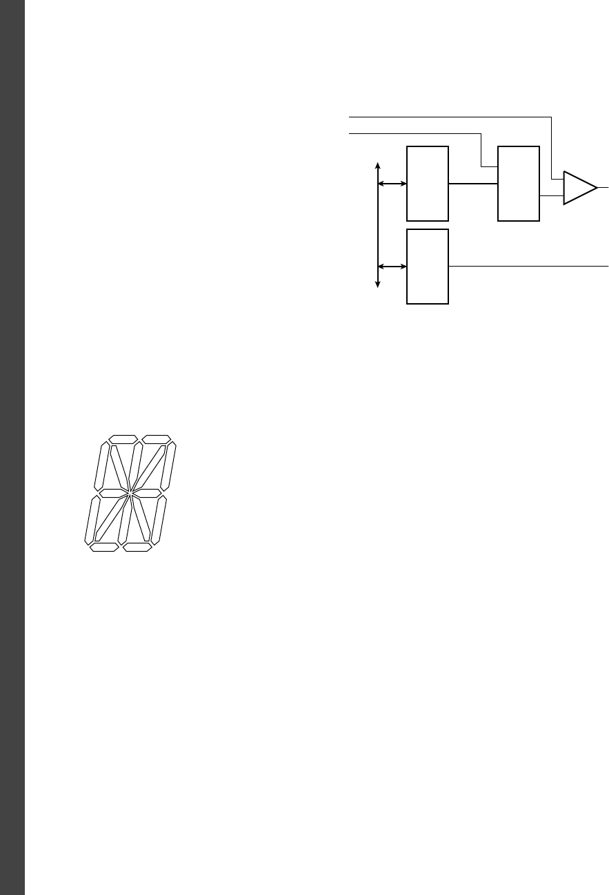
376 CHAPTER EIGHT i/o interfacing
binary amplitude value in r2 and outputs a corresponding value to an 8-bit
register at port address 28, connected to the cathodes of an 8-LED common-
anode bar display.
exercise 8.10 Draw a schematic of a circuit corresponding to the display
multiplexer of Example 8.2 on page 323.
exercise 8.11 A 16-segment LED display, shown in Figure 8.43, can
display alphabetic and numeric characters. Develop a circuit schematic and a
Verilog model of a display decoder and driver to drive a 16-segment common
anode LED display, given a 6-bit character-code input. Use a 64 16-bit ROM
to decode the input. You needn’t determine the ROM content for this exercise.
exercise 8.12 Modify the display multiplexer/decoder design of
Example 8.2 on page 323 to provide an 8-character alphanumeric scanned
display, with eight 6-bit character code inputs. Use the ROM described in
Exercise 8.11 to decode the character codes.
exercise 8.13 Design an output controller to drive eight solenoids.
The controller should have an 8-bit output register, and should connect to the
Wishbone bus used by the Gumnut core.
exercise 8.14 The ST Microelectronics L298 IC is a dual full-bridge
driver that can be used to drive the kind of stepper motor shown in Figure 8.12
on page 327. The connections between the L298 and the motor (in simplified
form) are shown in Figure 8.44. Determine the sequences of values on the inputs
to the L298 to drive the stepper motor clockwise and counterclockwise.
exercise 8.15 Assume the stepper motor driver described in Exercise 8.14
is connected to a Gumnut core through a 6-bit output register at port address 8,
with bits 0 to 5 of the register controlling signals
in1, in2, en_a, in3, in4 and en_b,
respectively. Write a Gumnut subroutine to step the motor one-quarter turn, either
clockwise, if r2 is 0, or counterclockwise, if r2 is 1. Hint: The subroutine will
need to keep track of the current state of the stepper motor control signals. Use a
location in memory to save the state.
+
–
DACoutput
data
register
input
status
register
Vin
Vf
Wishbone bus
(analog)
(analog)
FIGURE 8.42
A1 A2
B
C
D1D2
E
F
G
HJ
K
M
NP
R
FIGURE 8.43

exercise 8.16 Draw a diagram showing how the following components
might be used to construct a handheld voice recorder: microphone, microphone
amplifier, loudspeaker, loudspeaker amplifier, ADC, DAC, processor core,
instruction memory, data memory, push-button switches. The recorder has but-
tons to record, play/pause, stop, skip forward, and skip backward.
exercise 8.17 Draw a diagram similar to Figures 8.19 and 8.20 on
page 339 showing multiplexed bus connection of two data sources, two data
destinations, and two components that are both sources and destinations.
exercise 8.18 Revise Figure 8.21 on page 340 to omit the second ADC
controller.
exercise 8.19 Revise the Verilog model in Example 8.6 on page 341 to
omit the second ADC controller.
exercise 8.20 Revise the Verilog model of Example 8.8 on page 346 to
output X values if the enable inputs are Z or X.
exercise 8.21 Design a serial output controller for connection to the
Gumnut core using the Wishbone bus. The controller should transmit each 8-bit
data byte written to a data register using NRZ encoding with one start bit and
one stop bit, as shown in Figure 8.35 on page 355. Transmission should occur
at 9600 bits per second, with a transmit timing derived from a system clock
with frequency 39.321600MHz ( 9600 4096). When the stop bit has been
transmitted, the controller should set an interrupt request output. The interrupt
request output should be reset when the Gumnut
int_ack signal is 1.
exercise 8.22 Write a Gumnut subroutine to transmit a byte of data
using the serial output controller of Exercise 8.21. Assume the data register is
a port address 24 and that there are no other interrupt sources in the system.
The subroutine should wait in standby mode and not return until the controller
interrupts to indicate that the transmission is complete.
Exercises CHAPTER EIGHT 377
NN
SS
N
S
out1
L298
en_a
en_b
in1
in2
in3
in4
out2
out3
out4
+V
+V
FIGURE 8.44
378 CHAPTER EIGHT i/o interfacing
exercise 8.23 Revise the subroutine of Exercise 8.22 so that the subrou-
tine returns after having written the byte to the data register. This allows the pro-
cessor to continue with other work while the controller transmits the byte. You
will need to keep track of whether the controller is busy so that a subsequent call
to the subroutine does not overwrite the data register while transmission is still
in progress.
exercise 8.24 Develop a Verilog model of the serial output controller of
Exercise 8.21.
exercise 8.25 The OpenCores repository includes a UART core, uart16550,
that uses the Wishbone bus. (See http://www.opencores.org/projects.cgi/web/
uart16550/overview.) Develop a Verilog structural model of a system containing a
Gumnut core, instruction and data memories, and an instance of the UART core.
exercise 8.26 Draw a diagram similar to Figure 8.37 on page 356
showing Manchester encoding of the values 01100101 and 11110000.
exercise 8.27 Design a circuit that has, as input, a transmit clock and
an NRZ serial data signal (as in Figure 8.33 on page 354), and that generates a
Manchester encoded serial data signal as output.
exercise 8.28 Show how the system described in Example 8.11 on
page 359 would be extended to connect to four AD7414 sensors.
exercise 8.29 A Gumnut system includes a 4-digit 7-segment display,
connected as shown in Figure 8.45. The anode data register is at port address
128, and the cathode data register is at port address 129. Write Gumnut assem-
bly code for the
task_2ms subroutine described in Example 8.17 on page 369 to
scan the display. The BCD digits to display are stored in four bytes of memory
labeled
display_data. The subroutine should select one digit to drive each time it
is called. Thus, four successive calls are required for a complete scan.
+V
anode
data
register
cathode
data
register
Wishbone bus
FIGURE 8.45
379
accelerators
In Section 7.1, as part of our introduction to embedded computer organization,
we mentioned accelerators as optional components in embedded systems.
If the system must perform some operation faster than is possible with
embedded software running on a processor core, we can design custom
hardware to perform the operation at the required speed. In this chapter,
we will examine accelerators in more details and identify how they inter-
act with an embedded processor.
9.1 GENERAL CONCEPTS
Many operations performed by digital systems consist of a number of
steps. If a simple embedded processor core performs an operation, it per-
forms the steps in sequence, with each step using one or more proces-
sor instructions. The rate at which the processor can execute instructions
places a lower bound on the time it takes to perform the operation. The
key to accelerating performance is parallelism: performing multiple steps
at the same time, thus taking less time overall to complete the operation.
The cost of parallelism is the additional components needed to perform
the steps in parallel, since each component can only perform one step
at a time. However, if sequential execution does not meet performance
requirements, parallel hardware may be a higher-performance and lower-
power alternative to using a faster (and more expensive) processor.
One place in which we can add hardware to achieve parallelism is
within the processor core itself. As we saw in Chapter 7, a processor
repeatedly fetches, decodes and executes instructions. Many proces-
sor cores use various techniques to perform these steps in parallel. For
example, a processor might fetch a new instruction while decoding the
preceding instruction and executing the instruction before that. A higher
performance processor might fetch several instructions at once, decode
them together, and use multiple function units to execute as many of
them in parallel as it can. These and other techniques for achieving
9
380 CHAPTER NINE accelerators
instruction-level parallelism are described in textbooks on computer
architecture (see Section 9.5, Further Reading). While they can achieve
performance improvements ranging from 2 times to perhaps 20 times
over a simple processor core, the improvement comes at the cost of sig-
nificantly increased complexity, area and power consumption. If an appli-
cation requires much greater performance, or cannot afford the area and
power consumption of a high-performance processor, a custom hardware
accelerator may be a better option.
The extent to which we can improve performance depends on the
amount of parallelism we can achieve, that is, on the number of steps
we can perform at once. Many applications involve operations on data
that has a regular, repetitive structure, and in which computation steps
can be performed independently. For example, data from an audio source
is a regular sequence of sample values. An operation that implements a
volume control simply involves multiplying each sample value by the gain
value. If several sample values are available at once, they can all be mul-
tiplied by the gain value in parallel. Similarly, video data from a camera
consists of a sequence of frames, each of which is a rectangular array
of picture elements (pixels). Many video processing operations can be
performed within a frame in parallel across multiple pixels. Applications
that involve less regularly structured data, or data that arrives at irregular
intervals, are much harder to accelerate.
The amount of parallelism in some operations is limited only by the
amount of data available at a given time. This applies to operations where
each element of data can be processed independently of the others. Audio
volume control is such a case. Other operations, however, involve depen-
dencies that constrain parallelism. For example, some signal processing
operations on audio streams involve combining successive sample values
to produce values in a result stream. Filtering, as a case in point, involves
combining several successive sample values to yield a single value in the
output stream. Thus, we can’t complete the processing for a given output
sample until all of the required input values are available. Moreover, there
are intermediate results that must be computed as part of the process, and
the final result cannot be computed until all of the intermediate results
have been computed.
In summary, we can accelerate performance of an operation by repli-
cation of hardware resources to perform steps in parallel, up to the limits
on parallelism implied by the data dependencies and the availability of
data. Practical design of accelerators involves applying enough parallel-
ism to meet performance requirements, but not more, since that would
increase cost and power unnecessarily.
In order to identify opportunities for parallelism, we would typically start
with an abstract description of the processing operations to be performed by
the system. This might take the form of an algorithm description expressed

in a high-level language, such as a computer programming language or some
other formal notation. The description identifies the data to be processed,
how it is organized, and the sequence of processing steps to be performed.
We then need to identify a kernel of the algorithm, that is, a part that involves
the most intensive repetitive processing steps that take the most time. Such a
kernel is a good candidate for an accelerator, since improving performance
of the most time-consuming part of the algorithm gives the most payback.
The remainder of the algorithm can then be implemented in embedded
software.
We can quantify the performance gain achieved by accelerating a ker-
nel of an algorithm. Suppose a system takes some amount of time, t, to
execute the algorithm, and that a fraction, f, of that time is spent in exe-
cuting the kernel. The remaining fraction, 1 f, is spent executing code
other than the kernel. Thus,
t ft (1 f )t
If our accelerator speeds up execution of the kernel by a factor s, the time
spent in the kernel is divided by s, but the remaining time is unaffected.
Thus the total execution time for the algorithm is reduced to
t
f t
s
(1 f )t
The overall speedup is the ratio of the original time to the reduced time:
s
t
t
ft (1 f )t
ft
s
(1 f )t
1
f
s
(1 f)
This formula expresses Amdahl’s Law, named after Gene Amdahl, one
of the pioneers of parallel computing. It indicates that the overall effect
of speeding up a kernel depends strongly on the fraction of the original
time taken up in executing the kernel. If that fraction is small, even a large
speedup has little overall effect, since the nonaccelerated part dominates.
On the other hand, if the fraction is large, accelerating the kernel has sig-
nificant overall effect.
example 9.1 Suppose execution time is estimated for the various parts
of an algorithm on an embedded processor. The algorithm has two kernels, one
that consumes 80% of the execution time and another that consumes 15%.
Using a hardware accelerator, we could speed up execution of the fi rst kernel by
a factor of 10 or the second kernel by a factor of 100. Which accelerator gives
the best overall performance improvement?
9.1 General Concepts CHAPTER NINE 381
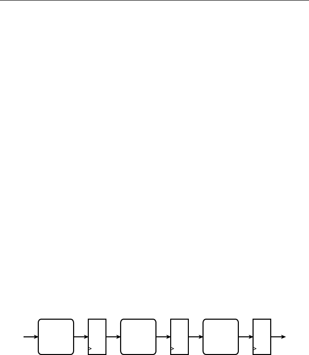
382 CHAPTER NINE accelerators
solution The overall speedup from accelerating the first kernel is
1
0.8
10
(1 0.8)
1
0.08 0.2
382
3.57
Accelerating the second kernel gives an overall speedup of
1
0.15
100
(1 0.15)
1
0.0015 0.85
1.17
Thus, even though the speedup for the second kernel is ten times that for the first
kernel, the lower fraction of the original execution time for the second kernel
means acceleration gives less overall improvement. Accelerating the first kernel is
more effective.
Within the kernel, we need to identify an order in which to perform
the computational steps. We need to ensure that data can be made avail-
able to be processed in order, and that intermediate results are computed
before they are needed for subsequent steps. Other than those constraints,
steps can potentially be performed in parallel. We finally need to determine
which steps will actually be performed in parallel to meet the performance
requirements. That then leads to an architecture for an accelerator, that is,
a description of the processing blocks and the data flow between them.
There are two main schemes for implementing parallelism in accelera-
tors. The first of these is simply to replicate components that perform a
given step so that they operate on different elements of data. The speedup
achieved through replication, compared to using just a single component,
is ideally equal to the number of times the component is replicated. This
scheme suits applications in which steps can be performed independently
on the different data elements.
The second scheme for implementing parallelism is to break a larger
computational step into a sequence of simpler steps, and to perform the
sequence in a pipeline, as shown in Figure 9.1. (We introduced the con-
cept of pipelining earlier in Section 4.1.1.) The pipeline stages perform
their simple steps in parallel, each operating on a different data element
or an intermediate result produced by the preceding stages. The overall
computation by the pipeline for a given data element takes approximately
the same time as a nonpipelined chain of components. However, provided
we can supply data to the pipeline input and accept data at the pipe-
line output on every clock cycle, the pipeline completes one computation
step 1 step 2 step 3
data
in
data
out
FIGURE 9.1 Pipelined
organization of an accelerator.
every cycle. Thus, the speedup compared to the nonpipelined chain is
ideally equal to the number of stages. This scheme suits applications that
involve complex processing steps that can be broken down into simpler
sequences with each step depending only on the results of earlier steps. In
some applications involving independent complex computations, we can
have replicated pipelines, giving the benefit of both schemes.
The analysis of systems, from algorithm description to accelerator
architecture, is done early in the system design flow. It is often performed
by expert system designers, drawing on their creativity and experience
with previous systems. Automating this form of analysis has proven to
be an extremely challenging problem, and early high-level synthesis tools
have not been successful, except within very narrow application domains.
More recently, a new generation of tools is starting to emerge and is show-
ing promise in a wider range of applications, especially in audio, video
and other signal-processing applications. As this technology matures, we
should expect to see wider adoption in design methodologies. We will
return to the topic of architecture analysis and its place in the design flow
in our methodology discussion in Chapter 10.
The data for many systems involving accelerators is input or output
data. In such systems, the I/O controller must transfer data between a
device and the embedded system’s memory at very high rates. Once the
data is in memory, it can be processed by an accelerator, with the results
also stored in memory. If these data memory accesses were mediated by
a processor, copying data between memory and registers under software
control, the rate of data transfer may be too slow. Instead, we can allow the
controller and the accelerator to perform direct memory access (DMA),
that is, to transfer data to and from memory autonomously. Instead of
the processor initiating a memory access, the I/O controller or accelera-
tor initiates an access, providing the required address and activating the
memory control signals.
Since the processor and any subsystems that perform DMA must
share access to the memory, and since the memory can only perform one
access at a time, we need to ensure that processor and DMA accesses
are interleaved. We must include an arbiter in the system, illustrated in
Figure 9.2, that makes sure subsystems take turns to access the memory.
Each master (the I/O controller, accelerator and processor) activates a
request signal to the arbiter when it needs to access the memory. The
arbiter decides among them, based on a predetermined policy, and acti-
vates a grant signal for one of the subsystems. That subsystem then pro-
ceeds with its access, with the memory responding as a slave. Any other
master with an active request must wait. When the granted master has
completed its memory access, it releases its request. The arbiter can then
activate another master’s grant. Different applications may use different
policies for deciding among competing requests, depending on whether a
9.1 General Concepts CHAPTER NINE 383
384 CHAPTER NINE accelerators
master can wait and for how long. Some applications use a round-robin
policy, in which masters are granted access in strict turn. Other systems
may require some masters to have priority over others in order to meet
requirements for processing rates.
In many applications, the data to be processed by an accelerator is
arranged in a regular pattern in memory, occupying blocks of adjacent or
regularly spaced locations. The job of the accelerator is to process the data
block by block. While it is processing one or more blocks, other parts of
the system may be working on other blocks. As an example, several algo-
rithms for processing still and video images divide each image into blocks
of 8 8 or 16 16 pixels and process each block independently. Similarly,
the MP3 format commonly used to encode audio data represents intervals
of sound in frames that can be processed independently.
The datapath for a block-processing accelerator needs two main
parts. The first part performs DMA to read and write data in memory.
It includes circuits for generating addresses, using the starting addresses
provided in registers by the processor and counters for keeping track of
progress. The second part of the data path performs the required com-
putation on the data. The control section for the accelerator sequences
operation of the data path and synchronizes operation with the processor.
Depending on the complexity of the operation and the bus protocol,
sequencing might be done with one finite-state machine or with separate
interacting machines for each activity.
Whereas a block-processing accelerator deals with blocks of data
stored in continguous memory locations, other forms of accelerators
deal with streams of data arriving in sequence from some source. Thus,
the two forms of accelerator are complementary: block processing deals
with sequences in space (data stored in memory), and stream processing
deals with sequences in time (data arriving at intervals). The source of
data for a stream-processing accelerator may be a high-speed input device
or another accelerator in a processing pipeline. Alternatively, data may
be fetched in a stream from memory for supply to an output device or
another accelerator.
processor
memory
arbiter
accelerator controller
request
grant
request
request
grant
grant
memory
bus
FIGURE 9.2 A multimaster
system with an arbiter for the
memory bus.
One of the most common application domains for stream-processing
accelerators is digital signal processing (DSP). One or more signals are
converted from analog to digital form, consisting of a stream of sample
values at periodic intervals. Processing operations include filtering, mixing,
applying gain or attenuation, and conversion between time and frequency
domains. Some application areas include audio and video processing,
radio and radar signal processing, and analysis of data from sensors. For
details of the mathematical basis for digital signal processing and the com-
putational techniques used, refer to Section 9.5, Further Reading.
Having provided a means for an accelerator to access data, either in
memory or through a stream connection, we also need to provide a way
for embedded software to control operation of the accelerator. This may
include providing data, such as parameters to be used in computations. It
also includes synchronizing operation of the accelerator with other activi-
ties in the system, such as arrival of data from I/O controllers or other
I/O events. Generally, this is done using input and output registers within
the accelerator. Embedded software can then interact with the accelerator
in much the same way as it interacts with autonomous I/O controllers.
For example, an accelerator might include registers for the address and
length of data in memory, for control of the operation to be performed
and for status. Embedded software could write to the registers to initi-
ate an operation, and rely on an interrupt from the accelerator when the
operation is complete.
In some applications, it may be possible for the processor and an
accelerator to operate with less strict synchronization. For example, the
processor might generate units of work for the accelerator to perform and
add information describing each unit to a first-in, first-out (FIFO) queue,
like that described in Section 5.2.3. The accelerator can then accept each
work unit when it is ready by reading the description from the head of the
FIFO queue. FIFO queues can also be used for communication between
multiple processors in a large-scale embedded system.
1. How does parallelism improve performance?
2. What factors constrain the amount of parallelism that can be
achieved?
3. What aspects are described by an algorithm?
4. Why is it best to accelerate a kernel of an algorithm?
5. If a pipeline has four stages and accepts new input data on every
clock cycle, what is the speedup compared to a nonpipelined chain
of components?
6. What is direct memory access (DMA)?
KNOWLEDGE
TEST QUIZ
KNOWLEDGE
TEST QUIZ
9.1 General Concepts CHAPTER NINE 385

386 CHAPTER NINE accelerators
7. What is the task of an arbiter in a multimaster system?
8. What is the distinction between a block-processing accelerator and
a stream-processing accelerator?
9. How does embedded software interact with an accelerator?
9.2 CASE STUDY: VIDEO EDGE-DETECTION
In this section, we will illustrate several aspects of accelerator design
using, as an example, an accelerator for edge-detection in video images.
This is somewhat of a compromise between what a real-world accelerator
might do and what can be included here without overwhelming detail.
Edge-detection is an important part of analyzing a scene in a video image,
and has application in many areas such as security monitoring and com-
puter vision. It involves identifying places in an image where there is an
abrupt change in intensity. Those places usually occur at the boundaries
of objects. Subsequent analysis of the edges can be used for recognizing
what the objects are.
For this example, we will assume monochrome images of 640 480
pixels, each of 8 bits, stored row-by-row in memory with successive pix-
els, left to right in a row, at successive addresses. Pixel values are inter-
preted as unsigned integers ranging from 0 (black) to 255 (white). We
will use a relatively simple algorithm, called the Sobel edge detector. It
works by computing the derivatives of the intensity signal in each of the
x and y directions and looking for maxima and minima in the deriva-
tives. These are the places where the intensity is changing most rapidly.
The Sobel method approximates the derivative in each direction for each
pixel by a process called convolution. This involves adding the pixel and
its eight nearest neighbors, each multiplied by a coefficient. The coeffi-
cients are often represented in a 3 3 convolution mask. The Sobel con-
volution masks, G
x
and G
y
, for the derivatives in the x and y directions,
respectively, are shown in Figure 9.3. We can think of the derivative image
being computed by centering each of the convolution masks over succes-
sive pixels in the original image. We multiply the coefficient in each mask
by the intensity value of the underlying pixel and sum the nine products
together to form two partial derivatives for the derivative image, D
x
and
D
y
. Ideally, we would then compute the magnitude of the derivative image
pixel as
D
_________
D
x
2
D
y
2
However, since we are just interested in finding the maxima and minima
in the magnitude, a sufficient approximation is
D D
x
D
y
–1
–2
–1
0
0
0
+1
+2
+1 –1 –2 –1
000
+1 +2 +1
G
x
G
y
FIGURE 9.3 Sobel
convolution masks.

This approximation works, because the square-root and square functions
are both monotonic (that is, they increase as the operand increases and
decrease as the operand decreases). Hence, the maxima and minima in
the true magnitude and the approximate magnitude occur at the same
places in the image. Computing the approximation involves much less
hardware than computing the square and square-root functions. We
repeat the computation of the approximate magnitude for each pixel
position in the image. Note that the pixels around the edge of the image
do not have a complete set of neighboring pixels, so we need to treat
them separately. The simplest approach is to set the value of D for
the edge pixels of the derivative image to 0. Since that is a relatively
straightforward process and is not time consuming, we can implement
it in software.
example 9.2 Express the Sobel edge-detection algorithm more formally
in a pseudo-code notation, that is, a notation like a computer programming
language.
solution We will use a pseudo-code notation like Verilog. Let O[row] [col]
denote pixels in the original image, and D[row] [col] denote pixels in the deriva-
tive image, where
row ranges from 0 to 479 and col ranges from 0 to 639. Also,
let
Gx[i] [j] and Gy[i] [j] denote the convolution masks, where i and j range from
–1 to 1. The algorithm is
for (row = 1; row <= 478; row = row + 1) begin
for (col = 1; col <= 638; col = col + 1) begin
sumx = 0; sumy = 0;
for (i = –1; i <= +1; i = i + 1) begin
for (j = –1; j <= +1; j = j + 1) begin
sumx = sumx + 0[row+i][col+j] * Gx[i][j];
sumy = sumy + 0[row+i][col+j] * Gy[i][j];
end
end
D[row][col] = abs(sumx) + abs(sumy)
end
end
example 9.3 Calculate the number of bits required to represent interme-
diate and final values for pixels in the Sobel convolution.
solution Each pixel is represented as an 8-bit unsigned number. Given
the coefficient values in the convolution masks, the partial products range from
–510 to 510. Thus, the partial products should be represented using 10-bit
signed numbers. There are nine partial products to add to form each of D
x
and
9.2 Case Study: Video Edge-Detection CHAPTER NINE 387
388 CHAPTER NINE accelerators
D
y
. However, the coefficient values are such that the result values range from
–1020 to 1020, which can be represented using 11 bits. We then need to add
the two absolute values, giving a range of 0 to 2040 for |D|, which can also
be represented in 11 bits. Since subsequent steps of the edge-detection operation
involve determining which derivative pixels are above a certain threshold, we
don’t need to maintain 11 bits of accuracy for the results. Instead, it is more con-
venient to scale the results back to 8-bit values, since they can be packed back
into memory in the same format as the original image.
example 9.4 Assuming a video frame rate of 30 frames per second, calcu-
late the rate at which computations must be performed.
solution Each frame consists of 640 480 307,200 pixels. Since there
are 30 frames per second, pixels must be processed at a rate of 307,200 30
9,216,000 per second, that is, approximately 10 million per second.
example 9.5 Identify the parallelism that can be exploited to obtain the
required performance.
solution The computations required for all of the derivative pixels are
independent of one another, since they only require values of the original image
pixels. Thus, we could perform computations for as many derivative pixels in
parallel as required. For computation of each derivative pixel, the data depen-
dency graph is shown in Figure 9.4. This diagram shows the data required for
each operation, starting with the pixels from the original image at the top, with
intermediate results feeding through to dependent operations, yielding the deriv-
ative pixel at the bottom. We’ve elided parti
al products in which the coefficient
is 0, since they don’t contribute to the result. Inspection of the diagram shows
that we can compute all of the partial products in parallel, since each partial
product depends only on an original pixel value and a constant coefficient. We
–1 +1 –2 +2 –1 +1
| |
+
+
+1 +2 +1 –1 –2 –1
| |
+
× G
x
D
x
|D|
× G
y
D
y
FIGURE 9.4 Data
dependency graph for computation
of a derivative pixel.
can then sum the two groups of six partial products in parallel, then compute the
two absolute values in parallel, before summing them to produce the derivative
pixel value.
The top-level view of the video system including the edge-detection
accelerator is shown in Figure 9.5. Video input comes from an I/O control-
ler for a video camera, which stores successive video frames in memory.
Software on the processor directs the accelerator to operate on a given
frame to produce the corresponding derivative image.
example 9.6 Suppose the memory in which the original and derivative images
are stored is 32 bits wide, and that each 8-bit byte is individually addressed. Video
frames are stored with one byte per pixel. The pixels of a row in a frame are stored
from left to right at successive addresses, and rows are stored top to bottom, one after
another in memory. Each memory read or write access takes 20ns, consisting of two
cycles of a 100MHz system clock. Can the memory access data fast enough?
solution Our earlier analysis showed that pixels arrive from the camera
at a rate of approximately 10 million per second, or one every 100ns. If the
video input controller stored each pixel to memory with a separate write access,
it would consume 20% of the available memory bandwidth. A better alternative
would be for the controller to aggregate four pixels and store them with a single
write access, reducing its share of the memory bandwidth to 5%.
The edge-detection accelerator needs to produce a derivative pixel at the same
rate at which input pixels arrive, that is, one every 100ns. Thus, writing the com-
puted derivative pixels would consume a further 5% of the memory bandwidth,
assuming groups of four derivative pixels are aggregated. Each pixel compu-
tation requires access to eight pixel values from the original image. A naive
approach would involve reading each pixel with a separate read operation, and
re-reading it when subsequently required to compute another derivative pixel.
This approach would require eight reads per computed pixel, requiring 160% of
the memory bandwidth. Clearly this is not possible.
Since each 32-bit word of memory contains four adjacent pixels in a row, we can
reduce the bandwidth required for reading by using as many pixels as we can
from each 32-bit read. For half the pixel positions, only three reads are needed
processor
memory
edge
detector
video
input
network
connection
FIGURE 9.5 A video system
incorporating an accelerator for
edge detection.
9.2 Case Study: Video Edge-Detection
CHAPTER NINE 389

390 CHAPTER NINE accelerators
(when the three pixels in each of the rows fall in the same word), and for the
other half of the pixel positions, six reads are needed (when the three pixels in
each of the rows cross word boundaries). So on average, each pixel computation
would require 4.5 reads, requiring 90% of the memory bandwidth. This is still
not feasible.
A further reduction can be afforded by noting that an original image pixel, once
read, is used to compute three derivative pixels in each of the following, same,
and preceding columns. So rather than re-reading it for those pixels, we can
store it within the accelerator for use in computing multiple derivative pixels.
We can save i
t just for computing the pixels to the left, in the same column,
and to the right. We only need to read three words for every fourth pixel being
computed, requiring 15% of the memory bandwidth. This, together with the
5% for video input and 5% for writing derivative pixels, is feasible, provided
the remaining 75% of the bandwidth is sufficient for other operations to be
performed by the system.
If we need to further reduce the bandwidth consumed by the edge detector, we
could include small memories in the accelerator to store complete rows read from
the main memory. This would allow each pixel to be read only once, reducing
the bandwidth required for reading pixels to just 5%. The total for video input
and edge-detection would then be 15% of the available bandwidth.
In our development of the edge-detector example, we will adopt the
approach of reading three rows of four adjacent pixels from the original
image and storing them in registers, rather than including memories for
whole rows. We will design the accelerator to process blocks of data,
where a block consists of the three complete rows of the original image
used to form a complete row of the derivative image. As we will see,
processing a block involves a start-up phase, a repetitive sequence of com-
putation, and a completion phase. These phases are repeated for each
derivative image row.
The architecture for the Sobel accelerator datapath is shown in
Figure 9.6. It is essentially a pipeline, with pixel data read from the origi-
nal image entering into the registers at the top right, flowing through the
3 3 multiplier array on the left, then down through the adders to the Dx
and Dy registers, then through the absolute value circuits and adder to the
|D| register, and finally into the register at the bottom left. The resulting
derivative pixels are then written from that register to memory. (While
a right-to-left data flow is opposite to usual practice, in this case, it has
the advantage of preserving the same arrangement of pixels as that in an
image.) We will describe the operation of the pipeline assuming initially
that it is full of data. We will then discuss how to deal with starting it up
at the beginning of an image row and draining it at the end of the row.
The pipeline generates the derivative pixels for a given row in groups
of four. The accelerator reads four pixels from each of the preceding,
current, and next rows in memory into the three 32-bit registers at the top
right of the figure. Each register consist of four 8-bit pixel registers. Over
the four subsequent clock cycles, pixels are shifted out to the left, one
pixel at a time, into the multiplier array. Each cell in the array contains
a pixel register and one or two circuits that multiply the stored pixel by
a constant coefficient value. Since the coefficients are all 1, 1, 2, or
2, the circuits are not full-blown multipliers. Instead, multiplying by 1
is simply a negator, multiplying by 1 is a through connection with no
circuitry, multiplying by 2 is a left shift of the result of a negator, and
multiplying by 2 is simply a left shift. On each clock cycle, the array
provides the partial products for a single derivative pixel, and the par-
tial products are added and stored in the Dx and Dy registers. Also, on
each clock cycle, the Dx and Dy values for the preceding pixel have their
absolute values computed and added and stored in the |D| register. The
| | + | |
+ +
+2
+2–2
–2–1
+1
–1 +1
+1 –1
data from
memory
data to
memory
current row
prev row
next row
result row
Dx
|D|
Dy
FIGURE 9.6 Architecture for
the Sobel accelerator datapath.
9.2 Case Study: Video Edge-Detection CHAPTER NINE 391
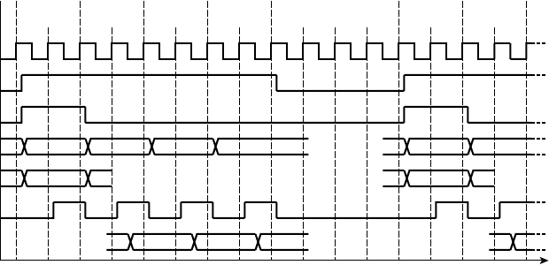
392 CHAPTER NINE accelerators
resulting derivative pixel values are shifted into the result row register.
When four result pixels are ready in the register, they are subsequently
written to memory.
In the steady state, during processing of a row, the accelerator needs
to write the pixels to memory from the result register before it can shift
new pixels into the multiplier array and the Dx, Dy and |D| registers.
Otherwise, the result values would be overwritten. Having written four
pixels, the accelerator can push four more pixels through the pipeline,
thus emptying the read registers and filling the result register. It can then
write those result pixels and read in three more groups of four pixels,
and repeat the process. This sequence is shown in Figure 9.7, assuming a
Wishbone bus connection with 32-bit-wide data signals and a 100MHz
clock, as suggested earlier. Since the accelerator is one of several masters
on the memory bus, it must request use of the bus for the writes and
reads and wait until granted access by the bus arbiter. We assume that the
arbiter gives the accelerator sufficiently high priority that it can use the
memory bandwidth it needs.
Now that we have considered the steady state during processing of
a row, we need to consider what happens at the beginning of a row. In
that case, the registers in the pipeline contain no valid data. So we start
processing a row as in the steady state, but omitting the write operation
for the first two iterations. Thereafter, the result register contains valid
data, so we include the write operation in each iteration. Note that after
the first four computation cycles, valid data has progressed into the pipe-
line as far as the Dx and Dy registers. After the second four computation
cycles, valid data has progressed as far as the right-most three result pixel
registers. The left-most result pixel register still contains invalid data.
clk
cyc_o,
stb_o
we_o
dat_o
ack_i
dat_i
adr_o
write
result
write
result
read
prev
read
prev
read
current
read
next
C1
pixel computation
C2 C3 C4
FIGURE 9.7 Timing of pixel
write and read operations and
computation in the pipeline.

However, this group of four pixel values is what we should write to the
beginning of the derivative image row. As we mentioned earlier, the left-
most position does not have a complete set of neighbors, so we don’t
compute a value for it. We will rely on the embedded software to clear
that pixel value to 0 subsequently.
When we reach the end of a row, we need to drain the pipeline. Since
the number of pixels in a row is a multiple of four (640 160 4), we can
always read complete groups of four pixels each. After reading the last
group, we perform four computation cycles normally. This gives us four
result pixels to write, plus three remaining pixel values in the pipeline.
We finish the row by writing the four result pixels, omitting the reads,
performing four further computation cycles to drain the pipeline and shift
the last pixel values into the required positions in the result register, and
performing a final write. Note that this places an invalid value in the
right-most result pixel register. This corresponds to the right-most pixel
of a row, which does not have a complete set of neighbors. Again, we will
rely on the embedded software to clear that pixel value to 0.
example 9.7 Develop Verilog RTL code to describe the datapath of
Figure 9.6.
solution The code in the module definition for the Sobel accelerator is
// Computation datapath signals
reg [31:0] prev_row, curr_row, next_row;
reg [7:0] O [-1:+1][-1:+1];
reg signed [10:0] Dx, Dy, D;
reg [7:0] abs_D;
reg [31:0] result_row;
...
// Computational datapath
always @(posedge clk_i) // Previous row register
if (prev_row_load) prev_row <= dat_i;
else if (shift_en) prev_row[31:8] <= prev_row[23:0];
always @(posedge clk_i) // Current row register
if (curr_row_load) curr_row <= dat_i;
else if (shift_en) curr_row[31:8] <= curr_row[23:0];
always @(posedge clk_i) // Next row register
if (next_row_load) next_row <= dat_i;
(continued)
9.2 Case Study: Video Edge-Detection CHAPTER NINE 393

394 CHAPTER NINE accelerators
else if (shift_en) next_row[31:8] <= next_row[23:0];
function [10:0] abs (input signed [10:0] x);
abs = x >= 0 ? x : –x;
endfunction
always @(posedge clk_i) // Computation pipeline
if (shift_en) begin
D = abs(Dx) + abs(Dy);
abs_D <= D[10:3];
Dx <= – $signed({3'b000, 0[–1][–1]}) // – 1 * 0[-1][-1]
+ $signed({3'b000, 0[-1][+1]}) // + 1 * 0[-1][+1]
– ($signed({3'b000, 0[ 0][-1]}) // – 2 * 0[ 0][-1]
<< 1)
+ ($signed({3'b000, 0[ 0][+1]}) // + 2 * 0[ 0][+1]
<< 1)
– $signed({3'b000, 0[+1][-1]}) // – 1 * 0[+1][-1]
+ $signed({3'b000, 0[+1][+1]}); // + 1 * 0[+1][+1]
Dy <= $signed({3'b000, 0[-1][-1]}) // + 1 * O[-1][-1]
+ ($signed({3'b000, 0[-1][ 0]}) // + 2 * 0[-1][ 0]
<< 1)
+ $signed({3'b000, 0[-1][+1]}) // + 1 * 0[-1][+1]
– $signed({3'b000, 0[+1][-1]}) // – 1 * 0[+1][-1]
– ($signed({3'b000, 0[+1][ 0]}) // – 2 * 0[+1][ 0]
<< 1)
– $signed({3'b000, 0[+1][+1]}); // – 1 * 0[+1][+1]
0[-1][-1] <= 0[-1][0];
0[-1][ 0] <= 0[-1][+1];
0[-1][+1] <= prev_row[31:24];
O[ 0][-1] <= O[0][0];
O[ 0][ 0] <= O[0][+1];
O[ 0][+1] <= curr_row[31:24];
O[+1][-1] <= O[+1][ 0];
O[+1][ 0] <= O[+1][+1];
O[+1][+1] <= next_row[31:24];
end
always @(posedge clk_i) // Result row register
if (shift_en) result_row <= {result_row[23:0], abs_D};
The first three always blocks in the module represent the three registers into
which groups of four pixels are read from memory. Each block has a separate
control signal governing loading, since the registers are loaded in successive
memory read operations. They share a control signal for shifting, since they all
shift a pixel out into the pipeline in parallel.
The next always block, as the comment suggests, represents the computational
pipeline of the accelerator. The signals to which the block assigns, governed by

the shift_en control signal, represent the pipeline registers. The signal O is a
3 3 array of pixel values, with indices corresponding to the difference in row
and column numbers from those of the derivative pixel computed from the reg-
ister values. For example, the element with indices [1][1] contains the pixel
in the previous row and next column from the pixel being computed. Values
are shifted into this array leftward from the left-most 8 bits of each of the input
registers. The Dx and Dy values are computed from the array element values. In
each case, the values are resized to 11 bits and converted to signed numbers, as
we discussed earlier in our analysis of the precision requirements for the com-
putation. Multi
plying by 2 is performed with a logical shift left by one position,
and multiplying by a negative coefficient is implemented by subtraction instead
of addition. The absolute values of the Dx and Dy values, implemented by the
abs function defined in the module, are added, and then scaled back from 11 to
8 bits to yield the final derivative pixel value.
The remaining always block represents the register that accumulates groups of
four derivative pixels for writing to memory. Pixels are shifted into this register
under control of the
shift_en signal.
We mentioned earlier that a block-processing accelerator needs cir-
cuits for address generation, as well as for processing the data. Our Sobel
accelerator needs circuits to compute the addresses for reading pixels
from the original image and for writing pixels to the derivative image. We
will provide a register into which the embedded software can write the
base addresses for the original image and the derivative image in memory.
The address generator needs to determine pixel addresses using the base
addresses. We will require that all addresses are word aligned, that is,
that they are all multiples of four. This means the two least significant
address bits are always 00, and so do not need to be computed or explic-
itly stored.
example 9.8 Given a base address B for an image in memory, derive
equations for computing the address of a pixel in row r and column c of the
image. Rows and columns are numbered from 0.
solution The image size is 480 rows of 640 pixels per row. The starting
address of row r is
B r 640
The pixel in column c in that row is then located at address
B r 640 c
We can treat the expression r 640 c as an address offset from the base address.
9.2 Case Study: Video Edge-Detection CHAPTER NINE 395

example 9.9 Design the address generator datapath for the Sobel accel-
erator. Assume main memory is 4Mbytes in size, organized as 1M 32 bits.
solution The address generator needs two base address registers: O_base,
for the original image, and
D_base, for the derivative image. Since pixels are
processed in groups of four, the least significant two address bits are always 0,
and so do not need to be explicitly stored in the address registers.
There are several alternatives for deriving the read and write addresses, including
maintaining counters for the image rows and columns. However, we can avoid the
need to multiply by 640 by counting pixel offsets from the base addresses, as shown
in Figure 9.8. In the case of the original image, we start counting from an offset of
0 and increment by 1 for each group of four pixels read from memory. We add the
offset to the base address to form the pixel-group address for the previous row. We
add 640/4 to that to form the read address for the current row, and add 1280/4 to
form the read address for the next row (assuming 00 for the least significant bits
in both cases). In the case of the derivati
ve image, we start counting from an offset
of 640/4 and increment by 1 for each memory write. The multiplexer in the figure
selects the appropriate computed address to drive the memory address bus.
example 9.10 Develop Verilog RTL code to describe the address generator
of Figure 9.8.
solution The code in the module definition for the Sobel accelerator is
O_base
O_prev_addr
adr_o
O_curr_addr
O_next_addr
640/4
1280/4
O_offset
cnt_en
reset
Q
D
CE
Q
+
+
+
D_base
D_addr
dat_i
O_base_ce
O_offset_cnt_en
D_base_ce
D_offset_cnt_en
offset_reset
clk
prev_row_load
curr_row_load
next_row_load
D_offset
cnt_en
reset
Q
D
CE
Q
+
clk
clk
clk
clk
FIGURE 9.8 Datapath for the
address generator.
396 CHAPTER NINE accelerators

// Address generator
always @(posedge clk_i) // 0 base address register
if (0_base_ce) 0_base <= dat_i[21:2];
always @(posedge clk_i) // 0 address offset counter
if (offset_reset) 0_offset <= 0;
else if (0_offset_cnt_en) 0_offset <= 0_offset + 1;
assign 0_prev_addr = 0_base + 0_offset;
assign 0_curr_addr = 0_prev_addr + 640/4;
assign 0_next_addr = 0_prev_addr + 1280/4;
always @(posedge clk_i) // D base address register
if (D_base_ce) D_base <= dat_i[21:2];
always @(posedge clk_i) // D address offset counter
if (offset_reset) D_offset <= 0;
else if (D_offset_cnt_en) D_offset <= D_offset + 1;
assign D_addr = D_base + D_offset;
assign adr_o[21:2] = prev_row_load ? 0_prev_addr :
curr_row_load ? 0_curr_addr :
next_row_load ? 0_next_addr :
D_addr;
assign adr_o[1:0] = 2'b00;
The always blocks commented as being base address registers represent the
base address registers for the original and derivative images, respectively. The
always blocks commented as being address offset counters represent the counters
for pixel groups read and written, respectively. The registers and counters are
governed by control signals generated by the accelerator’s control section. The
adders are represented by the combinational assignments to the four address
signals
O_prev_addr, O_curr_addr, O_next_addr and D_addr. The assignment to
the bus address signal
adr_o represents the multiplexer that chooses among the
generated addresses for memory read and write operations.
The remaining aspect of the Sobel accelerator design is control
sequencing. We have touched on the sequence needed for computation of
the derivative image, row-by-row and pixel-group at a time. This includes
sequencing of write and read operations with the accelerator as a bus
master. We also need to sequence the accelerator’s response as a bus slave
9.2 Case Study: Video Edge-Detection CHAPTER NINE 397
398 CHAPTER NINE accelerators
when the embedded software writes to the base address registers. Finally,
we need to provide for synchronization with the embedded software
controlling the accelerator. That requires some additional control and sta-
tus registers, as follows:
A control register that, when written to, causes the accelerator to
start processing an image. The value written is ignored.
A control register with an interrupt enable bit in bit 0.
A status register in which bit 0 is the done bit, set to 1 when the pro-
cessor has completed processing an image. Other bits are read as 0.
When the done bit is 1 and the interrupt enable bit is 1, the accelera-
tor requests an interrupt. Reading the done bit has the side effect of
acknowledging the interrupt and clearing the bit.
To keep the bus interface simple, we will map each of these registers at
32-bit aligned addresses. The complete register map is shown in Table 9.1.
register offset read/write
Interrupt control 0 write-only
Start 4 write-only
Original image base address 8 write-only
Derivative image base address 12 write-only
Status 0 read-only
example 9.11 Develop Verilog model code for the accelerator’s bus slave
interface.
solution The timing for the bus slave operations is shown in Figure 9.9.
Both write and read operations are initiated in a cycle where
cyc_i and stb_i are 1.
왘
왘
왘
TABLE 9.1 Register map for
the Sobel accelerator.
clk
cyc_i,
stb_i
we_i
dat_i
ack_o
dat_o
adr_i
slave
write
slave
read
FIGURE 9.9 Timing for slave
bus write and read operations.

In each case, the accelerator can respond by setting ack_o to 1 in the next cycle,
then back to 0 in the following cycle. We need to decode the bus address input to
derive a select signal for the accelerator, and use the less significant address bits to
determine which register to read or write. For write operations, we generate clock-
enable signals using combinational logic. In the case of a write to the start-register
address, since there is no real register, we derive a control signal,
start, that will
be used by the accelerator control section to initiate a computation sequence. For
read operations, we form the data value to be returned to the processor. The only
real register is the status register, for which we return the value of the
done bit,
zero extended to 32 bits wide. For other register offsets, we just return all zeros.
The read value is multiplexed with the value of the result row register to drive the
accelerator’s data output bus,
dat_o. The model code describing these aspects is
// Wishbone slave interface
assign start = cyc_i && stb_i && we_i && adr_i = = 2'b01;
assign 0_base_ce = cyc_i && stb_i && we_i && adr_i = = 2'b10;
assign D_base_ce = cyc_i && stb_i && we_i && adr_i = = 2'b11;
always @(posedge clk_i) // Interrupt enable register
if (rst_i)
int_en <= 1'b0;
else if (cyc_i && stb_i && we_i && adr_i = = 2'b00)
int_en <= dat_i[0];
always @(posedge clk_i) // Status register
if (rst_i)
done <= 1'b0;
else if (done_set)
// This occurs when last write is acknowledged,
// and so cannot coincide with a read of the
// status register.
done <= 1'b1;
else if (cyc_i && stb_i && we_i && adr_i = = 2'b00 && ack_o)
done <= 1'b0;
assign int_req = int_en && done;
always @(posedge clk_i) // Generate ack output
ack_o <= cyc_i && stb_i && !ack_o;
(continued)
9.2 Case Study: Video Edge-Detection CHAPTER NINE 399

400 CHAPTER NINE accelerators
example 9.12 Develop the control section to sequence computation of
the derivative image.
solution We can use a finite-state machine to sequence the computation.
Since much of the sequence is repetitive, we can use counters to keep track of
progress. We will use one counter to keep track of how many rows have been
computed, starting from 0 and incrementing up to 477. We will use a second
counter to keep track of iterations across the columns, starting from 0 and
incrementing up to 159. The state transition diagram for the FSM is shown in
Figure 9.10. We have only shown the states and the transition conditions to
avoid cluttering the diagram. Also, we have not shown transitions from a state
back to itself. We assume that if a transition condition from a given state is false,
the FSM stays in that state for the next cycle.
The FSM is initi
ally in the idle state. When the
start signal is activated by a write
to the start register, the FSM starts the initial sequence of reads and computa-
tions for the first row. This consists of reading the first three groups of original
image pixels and then performing four computation cycles. After that, the FSM
enters a loop in which it reads three more groups of original image pixels,
performs four computation cycles, and then writes a group of result pixels. As
we will see when we look at the output function of the FSM, the column counter
is incremented after each write. At the end of the last computation cycle, the
FSM either continues with the loop (if the column counter is not 158) or goes to
a state to start draining the pipeline (if the column counter i
s 158). Draining the
pipeline involves one state for writing the penultimate result group, four cycles
of computation, and one last state for writing the final result group. The row
counter is incremented after this final write. The FSM then goes back either to
the initial sequence for the next row (if the row counter is not 477) or to the idle
state (if the row counter is 477, the terminal count).
The output functions for the FSM are shown in Tables 9.2 and 9.3. To make
the tables a little easier to read, we have left entries blank where the control
outputs are 0, and only shown the cases where they are 1. Some of the control
signals are Moore outputs, depending on the current state only. They are shown
// Wishbone data output multiplexer
always @*
if (cyc_i && stb_i && !we_i)
if (adr_i = = 2'b00)
dat_o = {31'b0, done}; // status register read
else
dat_o = 32'b0; // other registers read as 0
else
dat_o = result_row; // for master write
idle
write_result read_prev read_curr read_next
comp1 comp2 comp3 comp4
start = 1
ack = 1 ack = 1
ack = 1
ack = 1 ack = 1 ack = 1
ack = 1
ack = 1
read_prev_0 read_curr_0 read_next_0
comp1_0 comp2_0 comp3_0 comp4_0
write_158 comp1_159 comp2_159 comp3_159 comp4_159
write_159
col = 158
col /= 158
ack = 1 and row /= 477
ack = 1 and row = 477
FIGURE 9.10 State
transition diagram for the Sobel
accelerator control section.
9.2 Case Study: Video Edge-Detection
CHAPTER NINE 401
in Table 9.2. Other control signals are Mealy outputs. For these, in Table 9.3,
we have shown the input conditions that, along with the current state, determine
their values. As in the state transition diagram, we have omitted the complemen-
tary conditions. In those cases, the Mealy outputs remain 0.
example 9.13 Develop Verilog model code for the control section.
solution The control-section code includes declarations of internal signals
for the control FSM, the row and column counters, and the control signals:
parameter [4:0] idle = 5'b00000,
read_prev_0 = 5'b00001,
read_curr_0 = 5'b00010,
read_next_0 = 5'b00011,
comp1_0 = 5'b00100,
(continued)

402 CHAPTER NINE accelerators
TABLE 9.2 Output functions
for the Moore control outputs of
the FSM.
current
state
offset_reset
row_reset
col_reset
prev_row_load
curr_row_load
next_row_load
shift_en
cyc_o
we_o
idle
111
read_prev_0
11 1
read_curr_0
11
read_next_0
11
comp1_0
1
comp2_0
1
comp3_0
1
comp4_0
1
read_prev
11
read_curr
11
read_next
11
comp1
1
comp2
1
comp3
1
comp4
1
write_result
11
write_158
11
comp1_159
1
comp2_159
1
comp3_159
1
comp4_159
1
write_159
11

9.2 Case Study: Video Edge-Detection CHAPTER NINE 403
TABLE 9.3 Output functions
for the Mealy control outputs of
the FSM.
current
state
condition
row_cnt_en
col_cnt_en
0_offset_cnt_en
D_offset_cnt_en
done_set
idle start = 1
read_prev_0 ack_i = 1
read_curr_0 ack_i = 1
read_next_0 ack_i = 1
1
comp1_0 –
comp2_0 –
comp3_0 –
comp4_0 –
read_prev ack_i = 1
read_curr ack_i = 1
read_next ack_i = 1
1
comp1 –
comp2 –
comp3 –
comp4 col /= 158
comp4 col = 158
write_result ack_i = 1
11
write_158
ack_i = 1
11
comp1_159 –
comp2_159 –
comp3_159 –
comp4_159 –
write_159 ack_i = 1 and row /= 477
11
write_159 ack_i = 1 and row = 477
11

404 CHAPTER NINE accelerators
comp2_0 = 5'b00101,
comp3_0 = 5'b00110,
comp4_0 = 5'b00111,
read_prev = 5'b01000,
read_curr = 5'b01001,
read_next = 5'b01010,
comp1 = 5'b01011,
comp2 = 5'b01100,
comp3 = 5'b01101,
comp4 = 5'b01110,
write_result = 5'b01111,
write_158 = 5'b10000,
comp1_159 = 5'b10001,
comp2_159 = 5'b10010,
comp3_159 = 5'b10011,
comp4_159 = 5'b10100,
write_159 = 5'b10101;
reg [4:0] current_state, next_state;
reg [9:0] row; // range 0 to 477;
reg [7:0] col; // range 0 to 159;
wire 0_base_ce, D_base_ce;
wire start;
reg offset_reset, row_reset, col_reset;
reg prev_row_load, curr_row_load, next_row_load;
reg shift_en;
reg row_cnt_en, col_cnt_en;
reg 0_offset_cnt_en, D_offset_cnt_en;
reg int_en, done_set, done;
The two counters used by the control section to keep track of progress through
rows and columns, respectively, are represented by the following always blocks:
always @(posedge clk_i) // Row counter
if (row_reset) row <= 0;
else if (row_cnt_en) row <= row + 1;
always @(posedge clk_i) // Column counter
if (col_reset) col <= 0;
else if (col_cnt_en) col <= col + 1;
Next, the model includes blocks representing the finite-state machine using the
techniques we have described in previous chapters. The state register is repre-
sented by the block:
always @(posedge clk_i) // State register
if (rst_i) current_state <= idle;
else current_state <= next_state;

A final always block combines both the state transition function and the output
function into the one block. The block also includes expressions comparing the
row and column counter values with their terminal count values, rather than
performing the comparisons in separate combinational statements. Combining
these aspects into a single block makes the Verilog model somewhat more com-
pact and simpler to understand, since the FSM is somewhat larger than those we
have previously described.
always @* begin // FSM logic
offset_reset = 1'b0; row_reset = 1'b0;
col_reset = 1'b0;
row_cnt_en = 1'b0; col_cnt_en = 1'b0;
0_offset_cnt_en = 1'b0; D_offset_cnt_en = 1'b0;
prev_row_load = 1'b0; curr_row_load = 1'b0;
next_row_load = 1'b0;
shift_en = 1'b0; cyc_o = 1'b0;
we_o = 1'b0; done_set = 1'b0;
case (current_state)
idle: begin
offset_reset = 1'b1; row_reset = 1'b1;
col_reset = 1'b1;
if (start) next_state = read_prev_0;
else next_state = idle;
end
read_prev_0: begin
col_reset = 1'b1; prev_row_load = 1'b1;
cyc_o = 1'b1;
if (ack_i) next_state = read_curr_0;
else next_state = read_prev_0;
end
read_curr_0: begin
curr_row_load = 1'b1; cyc_o = 1'b1;
if (ack_i) next_state = read_next_0;
else next_state = read_curr_0;
end
read_next_0: begin
next_row_load = 1'b1; cyc_o = 1'b1;
if (ack_i) begin
0_offset_cnt_en = 1'b1;
next_state = comp1_0;
end
else next_state = read_next_0;
end
comp1_0: begin
shift_en = 1'b1;
next_state = comp2_0;
end
...
comp4: begin
shift_en = 1'b1;
(continued)
9.2 Case Study: Video Edge-Detection CHAPTER NINE 405

406 CHAPTER NINE accelerators
if (col = = 158) next_state = write_158;
else next_state = write_result;
end
write_result: begin
cyc_o = 1'b1; we_o = 1'b1;
if (ack_i) begin
col_cnt_en = 1
'
b1; D_offset_cnt_en = 1
'
b1;
next_state = read_prev;
end
else next_state = write_result;
end
write_158: begin
cyc_o = 1
'
b1; we_o = 1
'
b1;
if (ack_i) begin
col_cnt_en = 1
'
b1; D_offset_cnt_en = 1
'
b1;
next_state = comp1_159;
end
else next_state = write_158;
end
...
write_159: begin
cyc_o = 1'b1; we_o = 1'b1;
if (ack_i) begin
D_offset_cnt_en = 1'b1;
if (row = = 477) begin
done_set = 1'b1;
next_state = idle;
end
else begin
row_cnt_en = 1'b1;
next_state = read_prev_0;
end
end
else next_state = write_159;
end
endcase
end
assign stb_o = cyc_o;
Now that we have developed all of the hardware required for the
Sobel accelerator, the remaining part is the embedded software that con-
trols its operation. As we mentioned when we introduced this example,
video edge-detection is used in a range of application areas. So rather
than redesigning the control software for each application, it makes bet-
ter sense to develop a software component that can be reused from one
application to another. We can do this by developing a driver that provides
a set of operations that gives application software an abstract view of the
accelerator. Each application can then use the driver as one part of a col-
lection of software components that implements the required functional-
ity. For example, an application that recognizes objects in video images
might apply edge-detection to each image in a video stream, followed by
grouping of edges and matching against a database of edge patterns. Such
software development is just as important as the hardware development
in a complete application. A more complete treatment can be found
in books on embedded system software development (see Section 9.5,
Further Reading).
1. If image pixels were represented using only 6 bits instead of 8, how
many bits would be required for the values of Dx, Dy and |D|?
2. Can the value of |D| for a given derivative-image pixel be computed
in parallel with the values of Dx and Dy? Why, or why not?
3. If the memory read and write time is increased from two cycles to
four, would there be suffi cient memory bandwidth for video input
and edge-detection?
4. Why do we not compute values for the left-most and right-most
pixels in each row of the derivative image?
5. How does the embedded software initiate processing of an image?
How does it determine when processing is complete?
6. What would happen if the software attempted to initiate processing
when processing of a previous image was not yet complete?
7. Is the FSM that sequences computation a Mealy, Moore, or hybrid
FSM?
9.3 VERIFYING AN ACCELERATOR
Throughout this book, we have stressed the importance of verification as
part of our design methodology. It is particularly important when design-
ing accelerators, given their relative complexity. We need to ensure that
the design will operate correctly with all legal data values, and that it
will interact with the embedded processor correctly. Since the space of all
possible data values and operational sequences is astronomically large, it
is not feasible to test the design exhaustively. Rather, we need to develop
a verification plan that covers a variety of operating conditions. We will
return to this in more detail in our methodology discussion in Chapter 10.
Meanwhile, we will illustrate a simpler approach to simulation-based
verification of the Sobel accelerator described in Section 9.2.
One way to approach verification of a complex accelerator is to verify
the different aspects of its operation independently. For example, we might
KNOWLEDGE
TEST QUIZ
KNOWLEDGE
TEST QUIZ
9.3 Verifying an Accelerator CHAPTER NINE 407

408 CHAPTER NINE accelerators
verify the following aspects of the Sobel accelerator one by one, adopting
a “divide and conquer” approach:
Slave bus operations
Computation sequencing
Master bus operations
Address generation
Pixel computation
Clearly all of these aspects of the accelerator must work correctly for
the accelerator as a whole to work. However, verifying each in turn is
much simpler than trying to verify all aspects at once. Having verified
that the slave bus operations function correctly, we can then use them to
initiate computation. Then we can check that computation follows the
intended sequence of steps, with master bus operations proceeding cor-
rectly, ignoring the actual addresses and pixel values. We can then make
sure addresses are being generated correctly, and finally check that pixel
values are computed correctly. Verifying a stream-processing accelerator
would proceed similarly, but we would additionally need to verify that the
accelerator interacts correctly with the source of data being processed.
For this verification process, we need to construct a testbench that
mimics the behavior of the embedded system containing the accelerator.
If we have a verified model of the embedded processor, we can include
it in the testbench and write small test programs to run on it. The test
programs write to accelerator registers to set up and initiate operations.
On the other hand, if no processor model is available, we can write a
bus functional model of the processor, that is, a model that performs a
predetermined sequence of bus operations without actually executing any
processor instructions. Our testbench also needs to include a memory
model and bus arbiter. The memory, like the processor, need not be a
fully functional model. Instead, it might simply engage in write and read
operations on the bus, generating read data according to a predetermined
rule and discarding write data. These simplifications allow us to focus
our verification effort on the accelerator, and to create test cases in a con-
trolled manner.
example 9.14 Develop a testbench for the Sobel accelerator that includes
a bus functional processor model. The processor should program the accelera-
tor to operate on an original image at address 008000
16
to generate a derivative
image at 053000
16
. It should then read the status register once every 10µs until
the
done bit is set. The testbench should also include a bus arbiter that gives the
accelerator priority, and a bus functional memory that returns 0 for reads and
discards data from writes.
왘
왘
왘
왘
왘

solution Our testbench is modeled after the general system organization
shown in Figure 9.2. The accelerator is the design under verification, and the
arbiter and bus functional processor and memory form the remainder of the test-
bench. We also include a clock and reset generator. The outline of the testbench
module definition is
`timescale 1ns/1ns
module testbench;
parameter t_c = 10;
parameter [22:0] mem_base = 23'h000000;
parameter [22:0] saobel_reg_base = 23'h400000;
parameter sobel_int_reg_offset = 0;
parameter sobel_start_reg_offset = 4;
parameter sobel_O_base_reg_offset = 8;
parameter sobel_D_base_reg_offset = 12;
parameter sobel_status_reg_offset = 0;
reg clk, rst;
wire bus_cyc, bus_stb, bus_we;
wire [3:0] bus_sel;
wire [22:0] bus_adr;
wire bus_ack;
wire [31:0] bus_dat;
wire int_req;
wire sobel_cyc_o, sobel_stb_o, sobel_we_o;
wire [21:0] sobel_adr_o;
wire sobel_ack_i;
wire sobel_stb_i;
wire sobel_ack_o;
wire [31:0] sobel_dat_o;
...
always begin // Clock generator
clk = 1'b1; #(t_c/2);
clk = 1'b0; #(t_c/2);
end
initial begin // Reset generator
rst <= 1'b1;
#(2.5*t_c) rst = 1'b0;
end
sobel duv ( .clk_i(clk), .rst_i(rst),
.cyc_o(sobel_cyc_o), .stb_o(sobel_stb_o),
(continued)
9.3 Verifying an Accelerator CHAPTER NINE 409

410 CHAPTER NINE accelerators
.we_o(sobel_we_o),
.adr_o(sobel_adr_o), .ack_i(sobel_ack_i),
.cyc_i(bus_cyc), .stb_i(sobel_stb_i),
.we_i(bus_we), .adr_i(bus_adr[3:2]),
.ack_o(sobel_ack_o),
.dat_o(sobel_dat_o), .dat_i(bus_dat),
.int_req(int_req) );
...
endmodule
The clock generator always block uses the parameter t_c for the clock cycle time,
giving a clock frequency of 100MHz. The parameters
mem_base and sobel_base
define the base addresses of the memory (000000
16
) and the Sobel accelerator
registers (400000
16
). Additional parameters define the offsets from the base
address for the control and status registers. Next, the testbench includes nets
for the bus address, data and control signals. As we will see shortly, these are
multiplexed from the various sources in the system. The testbench also declares
nets for connection specifically to the Sobel accelerator. Within the module, the
accelerator is instantiated as the design under verification (
duv) and connected to
the nets.
The testbench code for the processor bus functional model is
reg cpu_cyc_o, cpu_stb_o, cpu_we_o;
reg [3:0] cpu_sel_o;
reg [22:0] cpu_adr_o;
wire cpu_ack_i;
reg [31:0] cpu_dat_o;
wire[31:0] cpu_dat_i;
...
task bus_write ( input [22:0] adr, input [31:0] dat );
begin
cpu_adr_o = adr;
cpu_sel_o = 4'b1111;
cpu_dat_o = dat;
cpu_cyc_o = 1'b1; cpu_stb_o = 1'b1; cpu_we_o = 1'b1;
@(posedge clk); while (!cpu_ack_i) @(posedge clk);
end
endtask
...
initial begin // Processor bus-functional model
cpu_adr_o = 23'h000000;
cpu_sel_o = 4'b0000;
(continued)

cpu_dat_o = 32'h00000000;
cpu_cyc_o = 1'b0; cpu_stb_o = 1'b0; cpu_we_o = 1'b0;
@(negedge rst);
@(posedge clk);
// Write 008000 (hex) to 0_base_addr register
bus_write(sobel_reg_base
+ sobel_0_base_reg_offset, 32'h00008000);
// Write 053000 + 280 (hex) to D_base_addr register
bus_write(sobel_reg_base
+ sobel_D_base_reg_offset, 32'h00053280);
// Write 1 to interrupt control register (enable interrupt)
bus_write(sobel_reg_base
+ sobel_int_reg_offset, 32'h00000001);
// Write to start register (data value ignored)
bus_write(sobel_reg_base
+ sobel_start_reg_offset, 32'h00000000);
// End of write operations
cpu_cyc_o = 1'b0; cpu_stb_o = 1'b0; cpu_we_o = 1'b0;
begin: loop
forever begin
#10000;
@(posedge clk);
// Read status register
cpu_adr_o = sobel_reg_base + sobel_status_reg_offset;
cpu_sel_o = 4'b1111;
cpu_cyc_o = 1'b1; cpu_stb_o = 1'b1; cpu_we_o = 1'b0;
@(posedge clk); while (!cpu_ack_i) @(posedge clk);
cpu_cyc_o = 1'b0; cpu_stb_o = 1’b0; cpu_we_o = 1'b0;
if (cpu_dat_i[0]) disable loop;
end
end
end
The processor waits for completion of system reset, then performs the required
sequence of bus write operations to initialize the accelerator. For each bus
operation, described by the
bus_write task, the processor assigns the appropri-
ate values to the address, data and control signals, then waits for the accelera-
tor to acknowledge completion of the operation. After completion of the write
to the start register, the processor enters a loop in which it waits for 10µs,
resynchronizes with the clock, then reads the accelerator status register. When
the accelerator acknowledges completion of the read operation, the processor
checks whether the
done bit is 1. If so, the processor exits the loop, completing
the test.
9.3 Verifying an Accelerator CHAPTER NINE 411

412 CHAPTER NINE accelerators
The testbench code for the memory bus functional model is
wire mem_stb_i;
wire [3:0] mem_sel_i;
reg mem_ack_o;
reg [31:0] mem_dat_o;
...
always begin // Memory bus-functional model
mem_ack_o = 1'b0;
mem_dat_o = 32'h00000000;
@(posedge clk);
while (!(bus_cyc && mem_stb_i)) @(posedge clk);
if (!bus_we)
mem_dat_o = 32'h00000000; // in place of read data
mem_ack_o = 1'b1;
@(posedge clk);
end
The memory repeatedly waits until the bus_cyc and mem_stb_i signals are both
1, indicating that a memory operation is required. If
bus_we is 0, the operation
is a read, so the memory provides zeros on the data outputs. In the case of a
write operation, the memory does nothing with the input data. In either case, the
memory sets the acknowledge signal to 1, and then on the next clock cycle clears
the signal back to 0, completing the operation.
The arbiter for the testbench is somewhat more involved than the other
testbench components. It uses the
sobel_cyc_o and cpu_cyc_o signals as
requests from the Sobel accelerator and the processor, respectively, and
generates
sobel_gnt and cpu_gnt grant signals. When either of the request
signals is activated, the arbiter activates the corresponding grant. If both
requests are activated in the same cycle, the arbiter gives preference to the
accelerator, activating its grant and leaving the processor’s grant inactive until
the accelerator’s request is deactivated. Since the grant outputs depend not only
on the values of the request inputs, but also on the preceding history of request
values, the arbiter must be implemented as a sequential circuit using an FSM.
The state transition diagram is shown in Figure 9.11. The FSM is a Mealy
machine, since that allows us to activate a grant signal in the same cycle in
which the correspond
ing request is activated.
The testbench code for the arbiter is
parameter sobel = 1'b0, cpu = 1'b1;
reg arbiter_current_state, arbiter_next_state;
(continued)

sobel cpu
1, –
1, 0
1, 0
1, 0
0, 0
0, 0
0, 0
0, 0
sobel_cyc_o, cpu_cyc_o
sobel_gnt, cpu_gnt
0, 1
0, 1
–, 1
0, 1
FIGURE 9.11 State
transition diagram for the
testbench arbiter.
9.3 Verifying an Accelerator
CHAPTER NINE 413
reg sobel_gnt, cpu_gnt;
. . .
always @(posedge clk) // Arbiter FSM register
if (rst)
arbiter_current_state <= sobel;
else
arbiter_current_state <= arbiter_next_state;
always @* // Arbiter logic
case (arbiter_current_state)
sobel: if (sobel_cyc_o) begin
sobel_gnt <= 1'b1; cpu_gnt <= 1'b0;
arbiter_next_state <= sobel;
end
else if (!sobel_cyc_o && cpu_cyc_o) begin
sobel_gnt <= 1'b0; cpu_gnt <= 1'b1;
arbiter_next_state <= cpu;
end
else begin
sobel_gnt <= 1'b0; cpu_gnt <= 1'b0;
arbiter_next_state <= sobel;
end
cpu: if (cpu_cyc_o) begin
sobel_gnt <= 1'b0; cpu_gnt <= 1'b1;
arbiter_next_state <= cpu;
end else if (sobel_cyc_o && !cpu_cyc_o) begin
sobel_gnt <= 1'b1; cpu_gnt <= 1'b0;
arbiter_next_state <= sobel;
end else begin
sobel_gnt <= 1'b0; cpu_gnt <= 1'b0;
arbiter_next_state <= sobel;
end
endcase

414 CHAPTER NINE accelerators
The rest of the testbench code represents the bus multiplexers and slave select
logic:
wire sobel_sel, mem_sel;
...
// Bus master multiplexers and logic
assign bus_cyc = sobel_gnt ? sobel_cyc_o : cpu_cyc_o;
assign bus_stb = sobel_gnt ? sobel_stb_o : cpu_stb_o;
assign bus_we = sobel_gnt ? sobel_we_o : cpu_we_o;
assign bus_sel = sobel_gnt ? 4'b1111 : cpu_sel_o;
assign bus_adr = sobel_gnt ? {1'b0, sobel_adr_o} : cpu_adr_o;
assign sobel_ack_i = bus_ack & sobel_gnt;
assign cpu_ack_i = bus_ack & cpu_gnt;
// Bus slave logic
assign sobel_sel = (bus_adr & 23'h7FFFF0) = = sobel_reg_base;
assign mem_sel = (bus_adr & 23'h400000) = = mem_base;
assign sobel_stb_i = bus_stb & sobel_sel;
assign mem_stb_i = bus_stb & mem_sel;
assign bus_ack = sobel_sel ? sobel_ack_o :
mem_sel ? mem_ack_o :
1'b0;
// Bus data multiplexer
assign bus_dat = sobel_gnt && bus_we || sobel_sel && !bus_we
? sobel_dat_o :
cpu_gnt && bus_we
? cpu_dat_o :
mem_dat_o;
The grant signals from the arbiter determine which source provides values for
the bus control and address signals. They also gate the acknowledge signals
back to the masters, so that a master that is waiting for the bus does not receive
an acknowledgment from a slave for the active master’s bus operation. The bus
slave logic decodes addresses and determines which slave is selected. The select
signals gate the strobe signal from the active master to the selected slave, and
multiplex the selected slave’s acknowledgment signal onto the
bus_ack signal.
The bus data multiplexer determines the source of data for the
bus_dat signal,

depending on which master is active, which slave is selected, and whether the
bus operation is a read or a write.
We can simulate the testbench of Example 9.14 to verify that the Sobel
accelerator correctly responds to slave bus operations and performs master
bus operations with correct addresses. We need to observe the values of the
bus control and address signals, as well as the internal signals of the accel-
erator. Figure 9.12 shows a simulation waveform display of the bus sig-
nals during initialization of the accelerator by the processor bus functional
model. Figures 9.13 through 9.15 show the internal signals of the accelera-
tor during the start of processing a row (Figure 9.13), during steady state
processing (Figure 9.14), and upon completion of processing a row and
commencement of the next row (Figure 9.15). Finally, Figure 9.16 shows
the internal signals on completion of processing an entire image.
While the verification shown here might give us confidence that the
design is correct, it is by no means complete. For example, it doesn’t
demonstrate that the computation produces correct values according to
the specification of the algorithm, and it doesn’t show that the control
sequencing is correct for all possible interactions between the accelerator
and other bus masters. Creating test cases for simulation-based verification
to cover all of these aspects is infeasible, given the number of permutations
of data values and ways in which components can interact. Instead, we
need to turn to more sophisticated verification techniques, such as con-
strained random test generation, coverage analysis, and property-based
formal verification. We will return to the topic of verification again in
Chapter 10, but we also refer the interested reader to advanced books on
verification listed in Section 9.5, Further Reading.
9.3 Verifying an Accelerator CHAPTER NINE 415
000000 800004 C00004 000004 400004 00080
0
082800
0
00
0000
0
00
08
0
0
0
0
0
8
23500
0
1
0
00
0
00
0
000
00
000
0000
0
000
le
b
o
s
u
pc
le
b
o
s
02 03 0
4
05 06 07
0
8
09 001 011 021 031
klc/hcneb_tset/
tsr/hcneb_
t
set/
cy
c
_
s
u
b
/
hcn
e
b_tset
/
b
t
s_
s
ub/hc
n
eb_tset
/
ew_su
b
/
h
cne
b
_
t
s
e
t/
da_sub/hcneb
_
tset
/
r
000000 800004 C00004 000004 400004 00080
0
kca_sub/hcneb_tset/
t
a
d_
s
u
b
/
hc
neb_
t
set/
0
00
0000
0
00
08
0
0
0
0
0
8
23500
0
1
0
00
0
00
0
000
00
000
0000
0
000
i
_
b
ts_
le
b
o
s/hc
n
eb
_
tset
/
o
_
kc
a
_le
b
os
/
h
c
ne
b
_
ts
e
t
/
etat
s
_
t
n
err
u
c
_r
e
ti
br
a/hcn
e
b_t
s
et
/
le
b
o
s
u
pc
le
b
o
s
tn
g
_lebos
/
hcn
e
b_t
s
e
t
/
tng_upc/hcneb_tset/
les
_
le
b
o
s/hc
ne
b
_ts
et
/
le
s_m
e
m
/hcneb_tset/
FIGURE 9.12 Waveform
display of bus operations for
initializing the Sobel accelerator.
416 CHAPTER NINE accelerators
eldi 0_verp_d
a
e
r
0
_
r
ru
c
_daer
0
_tx
e
n_
d
aer
0
_1
p
m
oc 0_2pmoc
0_
3pm
o
c
0_
4
pmoc verp_daer
0
8
23
5
0 000
8
00 0828
0
0 005800 082350
4
0080
0
09 001 011 021 031 041 051 061 071 08
1
091 002
0
12
022
i_kl
c
/
v
ud
/h
cn
e
b_
tse
t/
eta
t
s_tn
e
rr
u
c/v
u
d/
hcn
e
b
_ts
e
t/
eldi 0_verp_d
a
e
r
0
_
r
ru
c
_daer
0
_tx
e
n_
d
aer
0
_1
p
m
oc 0_2pmoc
0_
3pm
o
c
0_
4
pmoc verp_daer
o_
c
yc/vud/h
c
ne
b
_
tset
/
o_e
w/
vud
/
hcneb_
t
set/
o
_
r
d
a/v
u
d/h
c
ne
b
_ts
e
t/
0
8
23
5
0 000
8
00 0828
0
0 005800 082350
4
0080
0
i
_k
ca/
vu
d/
hc
ne
b
_t
set
/
t
r
at
s/vud/hcneb_t
se
t/
t
e
s
e
r
_t
esf
f
o/vud/hcneb_t
s
e
t/
teser
_w
or
/
vud/hcn
e
b_ts
et
/
ne_tnc_wor/vud/hcneb_tset/
tes
e
r_l
oc
/
v
u
d/
hc
ne
b
_t
set
/
ne
_t
nc_loc/v
u
d/
h
cn
eb
_
tse
t/
ne
_t
nc
_t
es
ffo
_o
/v
ud
/hc
n
eb
_t
se
t
/
ne
_t
nc
_t
esf
fo
_d
/v
ud
/h
cn
eb
_t
se
t/
da
ol
_w
o
r
_
ve
r
p/v
u
d/
hc
ne
b
_ts
et
/
da
ol_w
o
r_rr
u
c/vu
d
/hc
n
eb
_t
s
et
/
d
aol
_w
o
r
_txe
n
/vu
d
/hc
n
eb_
t
s
e
t/
ne_tfih
s/
vud
/
hc
n
e
b_
ts
et/
t
es_enod
/
vu
d/
hc
ne
b
_t
s
e
t
/
qe
r_
t
n
i
/vu
d
/
hcn
e
b_tse
t
/
FIGURE 9.13 Waveform
display of accelerator internal
signals at the start of row
processing.
tlus
e
r
_e
ti
rw
v
e
r
p
_d
a
er
r
uc_
d
aer
r
txen_d
a
er
1
pm
o
c
2pmoc 3pm
o
c 4pm
oc
tl
user_et
ir
w
0823
5
0
80
0
80
0
8
8
2
8
00
805800 482350
013 023 033 043 053 063 073 083 09
3
0
04
0
14
024 034 044
i_kl
c/v
ud
/h
cn
e
b_
ts
et/
e
ta
t
s_tn
e
rr
u
c/v
u
d/
hcn
e
b_
ts
et/
tlus
e
r
_e
ti
rw
v
e
r
p
_d
a
er
r
uc_
d
aer
r
txen_d
a
er
1
pm
o
c
2pmoc 3pm
o
c 4pm
oc
tl
user_et
ir
w
o_
c
yc/vud/hcneb
_
t
s
et
/
o_e
w/
vu
d
/
hcn
e
b
_t
s
et/
o
_
r
d
a/v
u
d/h
c
neb_ts
e
t
/
0823
5
0
80
0
80
0
8
8
2
8
00
805800 482350
i
_k
ca/
vu
d/
hc
neb_t
set/
t
r
ats
/v
ud/hcneb_t
se
t/
t
e
ser
_t
esf
fo
/v
u
d/hcneb_t
s
e
t/
t
eser
_w
or
/v
ud/hcn
e
b_ts
et/
n
e
_tnc_w
or
/v
ud/
hcn
eb
_
tse
t/
tes
e
r_l
oc/
vu
d/h
c
n
eb
_t
set
/
ne
_t
nc
_l
oc/v
u
d/
h
cn
eb
_
tse
t/
ne
_tnc_t
esf
fo_
o
/v
ud
/hc
n
eb_
t
se
t
/
ne
_t
nc
_t
es
ffo
_d
/v
ud
/h
cn
eb
_t
se
t/
d
aol
_w
o
r
_ve
r
p/v
u
d/
hc
ne
b
_ts
et
/
da
ol_w
o
r_rr
u
c/vu
d
/
hcn
eb
_t
s
et
/
da
ol
_w
o
r
_txe
n
/vu
d
/hc
n
eb
_t
s
e
t/
ne_tfih
s/
vud
/
hcn
e
b_
ts
et/
t
es
_e
nod/v
ud/
hc
ne
b
_ts
e
t/
qe
r_
t
n
i
/vu
d
/
hcn
e
b_tset/
FIGURE 9.14 Waveform
display showing row processing
in the steady state.

9.3 Verifying an Accelerator CHAPTER NINE 417
4pmoc 851
_
eti
rw
951_1pmoc 951_2pmoc 951_3pmoc 951_4pmoc 951_etirw 0_verp_d
a
er 0
_
r
ru
c_daer
8F4
3
5
0
CF4
3
50 08
28
0
0
00
58
0
0
0
62
91
0
82
9
1
00
3
91
0
2391
04391
0
6391
08
3
91
i_klc/vud
/h
cn
e
b_tset/
eta
t
s_tn
e
rr
u
c/vud/
h
cneb_ts
e
t/
4pmoc 851
_
eti
rw
951_1pmoc 951_2pmoc 951_3pmoc 951_4pmoc 951_etirw 0_verp_d
a
er 0
_
r
ru
c_daer
o_
cyc/v
ud/hc
n
eb
_
t
s
et
/
o_
e
w/vu
d
/
hcn
e
b_
t
set/
o_
r
da/
v
u
d
/
h
c
ne
b
_tse
t/
8F4
3
5
0
CF4
3
50 08
28
0
0
00
58
0
0
i
_k
ca/
vu
d/
hc
n
e
b_tset
/
t
r
at
s/
vud/hcneb_t
se
t/
t
ese
r
_t
esf
fo
/v
ud
/hc
n
eb_t
s
e
t
/
t
es
e
r
_wo
r
/vu
d/
hc
n
e
b_ts
et/
ne
_tnc_w
or
/v
ud/
h
c
n
eb
_
tse
t/
tes
e
r_l
oc
/
v
u
d/
hc
ne
b
_t
set
/
ne
_t
nc_loc/v
u
d/
h
cn
eb
_
tse
t/
ne
_t
nc
_t
es
ffo
_o
/v
ud
/hc
n
eb
_t
se
t
/
ne
_t
nc
_t
esf
fo
_d
/v
ud
/h
cn
eb
_t
se
t/
da
ol
_w
o
r
_
ve
r
p/v
u
d/
hc
ne
b
_ts
et
/
da
ol_w
o
r_rr
u
c/vu
d
/hc
n
eb
_t
s
et
/
d
aol
_w
o
r
_txe
n
/vu
d
/hc
n
eb_
t
s
e
t/
ne_tfih
s/
vud
/
hc
n
e
b_
ts
et/
t
es_enod
/
vu
d/
hc
ne
b
_t
s
e
t
/
qe
r_
t
n
i
/vu
d
/
hcn
e
b_tse
t
/
FIGURE 9.15 Waveform
display showing completion of one
row and commencement of the next.
3pmoc 4
p
m
oc
8
5
1_
e
tirw 951
_
1pmoc 95
1
_2pmoc 951_3pmoc
9
51_4pmoc
951_
eti
rw
e
l
di
87DD9
0
C7D
D
90 08DD9
0
082350
04
7
691
9
06
769
1
9
087
69
1
9
00
8
6919
02
86
9
19
048
6
9
19
0
6
86
9
19
i_
k
lc/v
u
d
/
hcn
e
b_t
se
t/
et
a
t
s_
t
nerruc/vud/
h
cneb_tset/
3pmoc 4
p
m
oc
8
5
1_
e
tirw 951
_
1pmoc 95
1
_2pmoc 951_3pmoc
9
51_4pmoc
951_
eti
rw
e
l
di
o
_
c
yc/vud/
hc
ne
b
_
tset
/
o_ew
/
vu
d
/
hc
n
eb
_t
set/
o
_r
d
a/v
u
d/h
c
neb_tse
t/
87DD9
0
C7D
D
90 08DD9
0
082350
i
_k
ca
/
v
ud/hcn
e
b
_ts
et
/
trats/vud/hcneb_tset/
t
e
ser
_
tesffo/vud/hcneb_t
s
e
t/
tes
e
r
_wo
r
/v
ud/hcn
e
b_tset
/
n
e
_t
nc
_w
o
r/vu
d/hc
n
e
b_
ts
et
/
tes
e
r_l
oc/
vu
d
/hc
n
eb
_
tset/
ne
_t
nc_
l
oc/vud/
h
c
n
eb_tse
t
/
n
e_tnc_tesff
o
_o/
v
ud/hcneb_tse
t
/
n
e_t
n
c_t
esf
fo_
d
/v
ud
/h
c
neb_
t
se
t/
da
ol
_w
o
r
_ve
rp
/
vud
/
hcneb
_
tset
/
d
a
o
l
_
wor_
r
ru
c/v
ud
/hc
n
e
b_t
s
et/
d
aol
_w
or_tx
e
n/v
u
d
/hc
n
eb_
t
set/
ne_tfih
s/
vud/hc
n
e
b
_
ts
et/
t
e
s_e
n
o
d
/
v
ud/hcneb_t
s
e
t/
qe
r_
t
ni/vud/
hcn
e
b_t
s
e
t
/
FIGURE 9.16 Waveform
display showing completion of
image processing.
418 CHAPTER NINE accelerators
1. Is it possible to verify an accelerator design using exhaustive testing?
Why, or why not?
2. What is a bus functional model?
3. Given the arbiter in the testbench for the Sobel accelerator, what
happens if the accelerator and the processor both request use of the
bus in the same clock cycle?
4. What happens if the accelerator requests use of the bus while the
processor is currently granted use?
5. Does the testbench verify correct computation of derivative pixel
values?
KNOWLEDGE
TEST QUIZ
KNOWLEDGE
TEST QUIZ

9.4 CHAPTER SUMMARY
Parallelism, performing multiple processing steps at once, allows
accelerators to reduce the time required to complete an operation.
An accelerator achieves parallelism by replicating hardware
resources and by pipelining. This leads to cost/performance and
power/performance trade-offs.
The degree of achievable parallelism is constrained by data depen-
dencies within a computation.
Designing an accelerator involves analyzing an algorithm and identi-
fying a kernel to be implemented in hardware. The remainder of the
algorithm is implemented in embedded software.
Amdahl’s Law quantifies the overall speedup from accelerating a
kernel of an algorithm.
Accelerators and high-speed I/O controllers can use direct memory
access (DMA) to transfer data to or from memory without processor
intervention. An address generator in such a unit calculates memory
addresses for DMA.
An arbiter determines which of several bus masters can use the bus
at any time to access bus slaves, such as memory and I/O controller
registers.
A block-processing accelerator processes blocks of data stored in
memory. Many video and still-image processing applications are
block oriented.
A stream-processing accelerator processes data arriving from a
source in a sequence of values. Digital-signal processing (DSP) is
often stream oriented.
Accelerators include control and status registers for use by embedded
software.
Verification of an accelerator using exhaustive simulation is gener-
ally not feasible. Aspects of operation can be verified independently,
but a complete verification plan should include other forms of
verification.
9.5 FURTHER READING
Computer Architecture: A Quantitative Approach, 4th Edition, John L.
Hennessy and David A. Patterson, Morgan Kaufmann Publishers,
왘
왘
왘
왘
왘
왘
왘
왘
왘
왘
왘
9.5 Further Reading CHAPTER NINE 419

420 CHAPTER NINE accelerators
2007. An advanced textbook on computer architecture, covering
instruction-level parallelism in depth.
Parallel Computer Architecture: A Hardware/Software Approach, David
E. Culler and Jaswinder Pal Singh, Morgan Kaufmann Publishers,
1999. An in-depth treatment of parallel computing. While the book
focuses on parallel computers, many of the principles can also be
applied to architectures of hardware accelerators.
Understanding Digital Signal Processing, Richard G. Lyons, Prentice Hall,
2001. An introduction to the theory of digital signal processing (DSP).
Computers as Components: Principles of Embedded Computing System
Design, Wayne Wolf, Morgan Kaufmann Publishers, 2005. Includes
a discussion of accelerators in the context of embedded hardware
and software design, with a video-processing accelerator as a case
study.
Embedded Software Development with eCos, Anthony J. Massa, Pren-
tice Hall, 2003. Describes the Embedded Configurable Operating
System (eCos), including the hardware abstraction layer.
Comprehensive Functional Verification: The Complete Industry
Cycle, Bruce Wile, John C. Goss and Wolfgang Roesner, Morgan
Kaufmann Publishers, 2005. A detailed treatment of functional
verification strategies and techniques.
exercise 9.1 In computer graphics applications, a three-dimensional vec-
tor representing a point’s position in space can be transformed by multiplying by
a 3 3 matrix:
P
x
P
y
P
z
a
11
a
12
a
13
a
21
a
22
a
23
a
31
a
32
a
33
P
x
P
y
P
z
Determine the data dependencies in the computation and thus the maximum
available parallelism.
exercise 9.2 Devise a pipeline architecture that can perform the computa-
tion described in Exercise 9.1 using all the available parallelism. Assume a new
input vector arrives and a result can be accepted on every clock cycle.
exercise 9.3 If a kernel of an algorithm is accelerated by a factor of 100,
and the kernel accounts for 90% of execution time before acceleration, what is
the overall speedup?
EXERCISESEXERCISES
exercise 9.4 For a kernel that consumes 90% of execution time, what
speedup for the kernel would be required to achieve an overall speedup of 5?
exercise 9.5 Suppose there are two options for accelerating a kernel that
consumes 80% of a system’s execution time. Option 1 accelerates the kernel by a
factor of 100 and increases the system’s cost by a factor of 2. Option 2 acceler-
ates the kernel by a factor of 200 and increases cost by a factor of 4. What is the
ratio of cost to performance for each option, compared to the original system?
exercise 9.6 Use the Sobel convolution masks to compute the approxi-
mate derivative pixel at the center of each of the 3 3 image blocks shown in
Figure 9.17. The numbers represent the pixel intensities.
Exercises CHAPTER NINE 421
255 255
255
255
223
223
223
255 255
255 255 255
255 255 255 255 255 255 255
0
00 0
127
127
12763
63
191
191
191
191
191
127
127 127
FIGURE 9.17
exercise 9.7 Consider a lower-performance version of the Sobel accelera-
tor, dealing with video frames of 320 240 8-bit pixels at a rate of 15 frames
per second. Repeat the analysis of Example 9.6 to determine a suitable approach
to memory accesses for this version of the accelerator.
exercise 9.8 In Example 9.6, we mentioned that we could reduce the
memory bandwidth consumed by the Sobel accelerator by storing rows of pixels
in small memories, so that each pixel need only be read from memory once.
Revise Figure 9.6 to show how this might be done using two row memories.
Hint: It may simplify your design to assume that a memory can read and modify
a location in a single cycle, with the read data provided on the data output and
the new data taken from the data input. Memory components in some imple-
mentation fabrics can operate in this way.
exercise 9.9 Write a pseudocode outline (not detailed code!) of embedded
software for an edge-detection application using the Sobel accelerator. Assume
the camera input controller has a register for the base address in memory for
the next frame to be acquired, and interrupts the processor when the frame has
been acquired. The software should then use the accelerator to perform edge
detection. When the accelerator has completed its operation, the software should
perform a subroutine for post-detection analysis. The software should maintain
three images in memory: one being acquired from the camera, one being pro-
cessed by the accelerator, and one undergoing post-detection analysis.

422 CHAPTER NINE accelerators
exercise 9.10 Revise the memory bus functional model code to provide a
synthetic image (that is, an artificially constructed image) when locations in the
original image are read. The synthetic image should contain a 320 240 white
rectangle centered on a black background. Hint: use the memory address during
a read to determine whether the location being accessed is within the image. If
so, then calculate the row and column numbers from the address. If the row and
columns lie within the rectangle, the memory should return white pixel values;
otherwise, it should return black pixel values.
exercise 9.11 Calculate the values of the derivative pixels that should
result from Sobel edge detection of the synthetic image described in Exercise 9.10.
exercise 9.12 Write a checker always block for inclusion in the testbench
using the revised memory bus functional model of Exercise 9.10. The checker
should verify that derivative pixels written to memory by the Sobel accelerator
have the values determined in Exercise 9.11.
423
design methodology
Now that we have completed our coverage of design techniques for digital
systems, we return to the topic of design methodology that we introduced
in Chapter 1. If you have undertaken lab projects in conjunction with
studying this book, you will have put many of the ideas relating to design
and verification into practice. In this chapter, we will expand upon those
ideas and also consider the larger context in which digital systems are
designed.
10.1 DESIGN FLOW
In our introductory discussion of design methodology, we commented
that design of a real-world digital system is a complex undertaking, usu-
ally requiring a team of people. We stressed the importance of taking a
systematic approach in order to manage both the complexity of the design
itself and the many interactions between the participants. We introduced
the notion of a design methodology, which codifies the process of design,
verification and preparation for manufacture of a product. For the rela-
tively small projects we have described in this book, a systematic design
approach has been of some benefit. For large real-world projects, having
a clearly specified methodology and sticking to it are indispensable. Many
projects have failed, not through technical problems, but through lack of
control of the design process itself.
While many aspects of electronics design are standardized across the
industry, design methodology is not one of them. Indeed, it would be
difficult to settle on a standardized methodology, since there is significant
difference among design projects. Moreover, the suite of tools available to
designers evolves quite rapidly. Hence, each organization typically defines
its own methodology based on the kinds of the design projects it under-
takes, and evolves the methodology from project to project.
Our prototypical design methodology, introduced in Chapter 1,
divided the design flow into a number of stages: functional design,
10
synthesis, and physical design. Each stage includes verification steps to
ensure that the design meets its requirements and satisfies constraints.
Figure 10.1 shows the elements of the design flow, including hierarchi-
cal hardware/software codesign, integrated into a single diagram. The
product of the design process is a set of data files used in manufacturing
the product. Each manufactured unit is then tested and delivered to the
end customer or market. We also refined the design flow for embedded
systems to include design and verification of the embedded software.
N
Y
N
Y
OK?
Test
OK?
OK?
N
Y
H/W Integration
OK?
A
N
Y
Requirements
and
Constraints
N
YY
Software
Requirements and
Constraints
Hardware
Requirements and
Constraints
OK? OK?
N
AB
B
Synthesize
Post-synthesis
Verification
Physical
Implementation
Physical
Verification
Manufacture
H/W Unit
Design
H/W Unit
Verification
H/W Integration
Verification
S/W Unit
Design
S/W Unit
Verification
S/W Integration
S/W Integration
Verification
Architecture Exploration
and Partitioning
FIGURE 10.1 A prototypical
design fl ow, including hardware/
software codesign.
424 CHAPTER TEN design methodology
For many complex systems, the hardware is simply the platform upon
which to deliver the software, with most of the functionality of the system
implemented in the software. In such systems, developing the software is
a major proportion of the system development effort.
A key part of a design methodology is the set of electronic design
automation (EDA) tools used to support it. For nearly all designs, it is not
feasible to make physical prototypes to ensure that the design is correct
and meets constraints. Instead, we design models as virtual prototypes in
forms that EDA tools can analyze and refine. In the remainder of this sec-
tion, we will explore the stages of a design methodology in greater depth,
identifying the models we create, the kinds of analysis we perform, and
the EDA tools that we use. We will assume initially a linear flow, starting
from a design concept and following through to physical implementation.
In the subsequent section, we will consider how the process of design
optimization can cause us to return to earlier stages in the flow, leading to
a cyclic, evolutionary design flow.
10.1.1 ARCHITECTURE EXPLORATION
A digital system is designed and manufactured to meet some functional
requirements, subject to various constraints. Unless the system is a minor
modification to a previous design, there is a large space of possible designs
that could meet the requirements. Of those possible designs, some would
violate the constraints and so would not be feasible candidates. Others
would satisfy the constraints, so we would choose from among them. Our
choice is typically guided by one or more objective functions, such as cost,
performance, power consumption, or reliability, that we seek to optimize.
Of course, until we have undertaken some design effort, we have nothing
to analyze to determine whether a candidate design meets requirements
and satisfies constraints. Clearly we don’t want to go through the complete
design process for each candidate. Instead, we need to identify sufficient
information about a candidate at an abstract level to be able to estimate
the value of relevant properties of the system. The estimates don’t need
to be perfect, just sufficiently accurate to decide whether the candidate
would meet requirements and constraints, and to allow comparison of
candidates to select among them. We use the term architecture exploration,
or alternatively, design space exploration, to refer to the task of abstract
modeling and analysis of candidate designs. The term originates in the
concept of exploring the space of possible system architectures.
One important aspect of architecture exploration is partitioning of
operations among components of a system. Partitioning is essentially
the application of a divide-and-conquer problem-solving strategy. If our
system requirements involve a number of processing steps, we can divide
our system into a number of components, each of which performs one
10.1 Design Flow CHAPTER TEN 425
426 CHAPTER TEN design methodology
of the processing steps. The components interact with one another to
complete the overall task of the system. When working at the abstract
level of architecture exploration, the components need not be physical
parts of the system. Instead, we can think of logical partitioning, that
is simply identifying parts of the system that will implement the vari-
ous processing steps. This form of partitioning is also called functional
decomposition. We can also think about the kinds of physical components
that we might include in the system and how the logical partitions can
be mapped to the physical partitions. The physical partitions can include
processor cores, accelerators, memories and I/O controllers. Also impor-
tant is hardware/software partitioning. We addressed this as part of our
discussion of accelerator design in Section 9.1. A given logical component
may be mapped to a specialized hardware component whose only task is
to implement that logical component. Another logical component may
be mapped to a software task run on a processor core under control of a
real-time operating system.
As an example of system partitioning, consider a road transport mon-
itoring system that checks whether freight trucks drive from one part of
the country to another in too short an interval. (Such a system is deployed
in the author’s neighborhood in Australia.) Stations on freeways each have
a video camera on a gantry over the road. The video images are analyzed
to identify the license plate of each truck passing underneath, and the
time and license number are logged. The information is transmitted to a
central facility for recording and comparison with information from other
stations. A hypothetical functional decomposition of the monitoring sta-
tion is shown at the top of Figure 10.2. It includes logical components for
input of video from a camera, filtering to remove noise, edge-detection,
Video
Input
Video
Filter
Video
Filter
Edge
Detect
Edge
Detect
Shape
Detect
Shape
Detect
Plate
Detect
Plate
Recog
Log
Network
Interface
Network
Interface
System
Control
Diag/
Maint
Video
Memory
Memory
Processor
Core
Bus
Bridge
Video
Input
Video Bus
Processor Bus
FIGURE 10.2 Logical
partitioning (top) and physical
partitioning (bottom) of a transport
monitoring system.
shape detection, license plate detection, character recognition to identify
the license number, logging, network interface, system control, and
diagnostic and maintenance tasks. This logical structure can be mapped
onto the physical structure shown at the bottom of Figure 10.2. In this
case, the physical components comprise an embedded system with accel-
erators for video processing up to the shape-detection stage. License plate
detection and recognition, logging, system control, and diagnostics and
maintenance tasks are mapped onto software tasks running on the proces-
sor core.
As we mentioned in Section 9.1, architecture exploration and parti-
tioning is often done by expert system designers. Decisions made in this
early stage of the design flow have a major impact on the rest of the
design. Unfortunately, it is very difficult to automate these tasks using
EDA tools. Instead, system designers often rely on ad hoc system models,
expressing algorithms in programming languages such as C or C, and
using spreadsheets and mathematical modeling tools to analyze system
properties. By far the most valuable asset in this stage is the experience
of the system designer. Lessons learned from previous projects can be
brought to bear on new design projects. Nonetheless, design automation
for architecture exploration and system-level modeling has been an active
area of research for some time, and we should expect tool support to
improve from its present immature state.
However architecture exploration design is done, whether by system-
atic or ad hoc means, the result is a high-level specification of the system.
For each of the components in the system, the specification describes the
function it is to perform, the connections to other components, and the
constraints upon its implementation. The specification might be expressed
in a language that can be executed or simulated, such as certain forms of
the Unified Modeling Language (UML). Such an executable specification
has the benefit of being more precise than a specification written in a nat-
ural language, such as English. Moreover, execution can answer questions
of interpretation, such as what a component is supposed to do in certain
circumstances. The specification is used as the input to the next stage of
the design flow.
10.1.2 FUNCTIONAL DESIGN
The next stage to consider is functional design, which has been the main
topic of this book. Our architecture specification has decomposed the
system into physical components, each of which must implement one
or more logical partitions. As we mentioned in Chapter 1, architectural
design is the top level of a top-down design process. We can decompose
each component into subcomponents, which we then design and verify
as units. That might also involve further decomposition, until we reach a
level of complexity that is manageable.
10.1 Design Flow CHAPTER TEN 427
428 CHAPTER TEN design methodology
Before we embark on that division into subcomponents, we can
develop a behavioral model of the component, expressing its functionality
at an intermediate level of abstraction between system level and register-
transfer level. The behavioral model might include a description of the
algorithm to be implemented by the component without detailed cycle-
by-cycle timing, or it might just be a bus functional model. The purpose
of the behavioral model is to allow function verification of the component
before proceeding to detailed implementation. Once the functionality is
verified, the same testbenches can be used with the detailed implementa-
tion models to verify them under the same test cases. As an example, con-
sider the Sobel edge-detection accelerator that we discussed in Chapter 9.
We presented a pseudo-code description of the algorithm in Example 9.2
on page 387. We could develop a behavioral model of the edge-detec-
tor based on that algorithm. While the behavioral model might read and
write pixels in a different order and with different timing, they should
produce the same derivative image from a given original image.
In order to implement a given component, we can take several
approaches. One approach is to design a new implementation by refining
the higher-level model, using the design techniques we have discussed in
previous chapters. An alternative, however, is to reuse a component from
a previous system, from a library of components, or from a component
vendor, if a suitable reusable component is available. We often use the
term intellectual property, or IP, to refer to such reusable components,
since they constitute a valuable intangible resource. The most obvious
benefit of reuse is the saving in design time it affords. Moreover, if the IP
has been specifically developed for reuse and has been thoroughly verified
as a unit, then we can save effort in verification. Even if an IP block
does not exactly meet the requirements for our system, we may be able
to adapt it with less effort than would be required for a fresh start. If the
IP performs the required function, but does not have quite the right inter-
face connections or timing, we might be able to embed it in a wrapper,
circuitry that deals with the differences. If the IP has almost the required
function and the source code is available to us, we might be able to make
minor changes to adapt its functionality to our needs.
In circumstances where there is no reusable IP available and we must
implement a component from scratch, we should still think of reuse. We
should consider whether the component might be reused in a subsequent sys-
tem. In that case, we should spend extra effort to ensure that the component is
well specified, its functionality is verified under all operating conditions, and
its use and implementation are well documented. The effort spent doing that
when developing the component will be recouped in the subsequent projects.
Another alternative for implementing a component may be to use a core
generator, which is an EDA tool that generates a model of a component based
on parameters that describe its function. Core generators are available for
common kinds of functions, such as memories, arithmetic units, bus interfaces,
10.1 Design Flow CHAPTER TEN 429
digital signal processing, and finite-state machines. Figure 10.3 is a screenshot
of a typical core generator, in this case a tool provided by Xilinx for generating
cores to be implemented in its FPGAs. (The Xilinx Core Generator is included
as part of the Xilinx ISE tool suite linked from the companion website.) The
screenshot shows the kinds of core function that can be generated. For each
function, parameters controlling operation of the generated core can be speci-
fied, as illustrated in Figure 10.4 for a content-addressable memory core. The
tool then automatically generates a suite of design files for the specified func-
tion, including HDL source code for behavioral simulation and net-list files
for inclusion in the physical design. Core generators are available for ASIC-
based designs as well as for FPGAs. In both cases, using a generated core can
save a substantial amount of design and verification effort, and is well worth
considering.
Throughout this book, we have shown how to design components
using the Verilog hardware description language. Verilog has much in
common with computer programming languages, and many of the same
considerations apply to managing the design process. In particular, it is
important to write Verilog models in such a way that they are clearly
understandable and can be maintained throughout their life cycle. Many
organizations adopt coding style rules to help ensure the quality of the
model code. Some EDA vendors also provide style checking tools, some-
times called lint tools (after the Unix lint program for checking C pro-
grams) that verify whether code meets a set of rules.
Another aspect of hardware model development in common with
software development is the need for revision management, also referred
to as source code control. Usually, there are multiple designers working
on the model code for a component, and they make numerous revisions
as they develop and verify the code. Revision management software helps
coordinate their work by maintaining a repository of versions of the
code. Typically, designers work with their own copy of the code. As they
complete a change, they commit the revised code back to the repository.
Other designers periodically update their copies with changes commit-
ted to the repository. Usually, changes made by different designers affect
different parts of the code, so the changes can be merged automatically.
Where changes conflict, the designers must manually reconcile them. Some
vendors’ EDA tool suites include proprietary revision management tools.
Others use open source tools, such as the Concurrent Version System (CVS)
or the more recent Subversion tool. The author has used both of these to
good effect, for software development, digital design, and other projects.
10.1.3 FUNCTIONAL VERIFICATION
Throughout this book, we have stressed the importance of verification
of digital designs, focusing mainly on simulation-based verification of
functionality. We have shown how to construct testbenches that stimulate a
430 CHAPTER TEN design methodology
FIGURE 10.3 Xilinx Core
Generator showing categories of
core functions.
FIGURE 10.4 A dialog
for specifying parameters for a
generated core.
design under verification and that include checkers to monitor outputs of the
design. Successful verification of a system requires a verification plan that
identifies what parts of the design will be verified, the functionality that will
be verified, and how verification will be performed. Without a verification
plan, there are no criteria to determine whether verification is complete.
The first question, what parts to verify, can be answered by appealing to
the hierarchical decomposition of the system. Since the system is composed
of subsystems, each subsystem must be correct for the entire system to be cor-
rect. Thus, verifying each subsystem can be considered to be a prerequisite for
verifying the entire system. This argument can be repeated recursively, leading
to a bottom-up verification strategy. As each designer works on a bottom-
level component, they verify that it meets its functional requirements. Those
components can then be integrated into the next-level subsystem, which is
then verified. The process is repeated, up to the top level of the system.
The second question, what functionality to verify, can be answered
by appealing to the specification for each component. That, in itself, is
good motivation for ensuring well-written specifications. Without a clear
statement of what a component is supposed to do, we cannot verify with
confidence that the component does what is required of it. At the lower
levels of the design hierarchy, the functionality of each component is rela-
tively simple, and so the component can be verified fairly completely. At
higher levels of the design hierarchy, the functionality of subsystems and
the complete system gets much more complex. Thus, it is much harder to
verify that a subsystem or the system meets functional requirements under
all circumstances. Instead, we might focus on the interactions among
components, for example, checking for adherence to protocols.
We use the term coverage to refer to the proportion of functionality that
is verified. Historically, code coverage has been used as a figure of merit.
It refers to the proportion of lines of code that have been executed at least
once during simulation of the design. The benefit of using code coverage is
that it is easy to measure, but it does not give a reliable indication that all
of the required functionality has been implemented and implemented cor-
rectly. Instead, we should use functional coverage, even though it is harder
to quantify. Aspects of functional coverage include the distinct operations
that have been verified, the range of data values that have been applied, the
proportion of states of registers and state machines that have been visited,
and the sequences of operations and values that have been applied. Cover-
age measurement tools are now available that allow monitoring of signal
and storage values within a model during simulation and measurement
of which ranges of values have been observed. These tools can help us to
identify operating conditions that have and have not been verified.
The third question in the verification plan is how to verify. There are
a number of techniques that we can apply. We have already illustrated
the approach of directed testing using simulation in several examples
throughout this book. Directed testing involves identifying particular test
10.1 Design Flow CHAPTER TEN 431
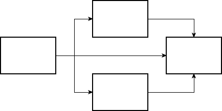
432 CHAPTER TEN design methodology
cases to apply to the DUV and checking the output for each test case. This
approach is very effective for simpler components where there are only
a small number of categories of stimulus. However, for more complex
components, achieving significant function coverage is not feasible, and
so we must complement directed testing with other techniques. Another
approach that has gained acceptance is constrained random testing. This
involves a test case generator randomly generating input data, subject to
constraints on the ranges of values allowed for the inputs. Specialized
verification languages, such as Vera and e, include features for specifying
constraints and random generation of data values to be used as stimulus
to a DUV. More recently, similar features have been included in System-
Verilog, an extension to Verilog. Similar features are also planned for inclu-
sion in a future revision of the VHDL hardware description language.
Both directed and constrained random testing require checkers that
ensure that the DUV produces the correct outputs for each applied test case.
If, as part of our top-down design process, we have developed a behavioral
model of a component, we may be able to use it to simplify the checker for
the register-transfer level implementation. We can create a comparison tes-
tbench, illustrated in Figure 10.5, that verifies that the implementation has
the same functionality as the behavioral model. We use the same test-case
generator to provide test cases to two instances of the design under verifi-
cation: one an instance of the behavioral model, and the other an instance
of the RTL implementation. The checker then compares the outputs of the
two instances, making any necessary adjustments for timing differences.
Directed and constrained random testing are both simulation-based
verification techniques. The problem inherent in simulation-based verifi-
cation is that it is not feasible to attain 100% coverage. The number of
possible input cases and sequences is too large for exhaustive simulation
to be feasible. Formal verification, on the other hand, allows complete
verification that a component meets a specification. The specification is
embodied in one or more asserted properties, expressed in a property
specification language, such as PSL (see Section 10.7, Further Reading).
PSL can be used as an adjunct to a hardware description language such
as VHDL or Verilog. The recent revision of VHDL also allows PSL to be
embedded in a VHDL model, either as part of the design or in a testbench
DUV
Behavioral
Model
DUV
RTL
Model
Test Case
Generator
Checker
FIGURE 10.5 A comparison
testbench for comparing outputs
of a behavioral model and its RTL
refi nement.
model. As an alternative, the SystemVerilog extension of Verilog includes
features similar to those of PSL for expressing properties.
A property can be as simple as a Boolean expression relating the values
of signals in the design. More commonly, it involves temporal expressions
relating sequences of values over time. For example, a property might specify
that activation of a select signal followed by an enable signal on the next
clock cycle is followed by activation of an acknowledge signal within three
clock cycles and deactivation of all three signals on the subsequent cycle.
A formal verification tool performs state-space exploration to verify the
asserted properties. It exhaustively examines all possible sequences of input
values, determines the resulting values for signals in the design at all clock
cycles, and checks that the asserted properties hold for all cycles. Where a
property does not hold, the tool uses the sequence of input values to con-
struct a counter-example leading to the failure. Properties can also be used to
express assumptions about the inputs to a component, which help the formal
verification tool limit the space of possible values that it has to explore.
The strength of formal verification is that it provides a rigorous proof
that the assertions hold. However, its completeness is only as good as the
properties that are verified. If those properties do not cover all of the func-
tional requirements, then a formal verification does not achieve complete
functional coverage. Moreover, writing properties that completely and
accurately capture the intent of a specification is very difficult. In many
organizations using formal verification, that task is left to expert verifica-
tion engineers who work alongside design engineers. A further difficulty
is that state-space exploration is a computationally intense problem, so
verification of numerous complex assertions may be intractable. It may
be necessary to limit the use of formal verification to parts of a design or
to a subset of the complete functionality, and to use other techniques for
other parts.
While properties are a necessary part of formal verification, they can
also be used in simulation-based verification of a system. In particular, a
property can be used to generate a checker that monitors the values of
signals mentioned in the property during the course of a simulation and
tests whether the property holds. One way to generate such a checker
is to automatically translate the property into an HDL model that can
be simulated along with the functional model. Alternatively, a simulator
that supports the property language can directly interpret the property
during simulation, in which case the checker is implied by the property.
The advantage of this approach to verification using properties is that the
properties are often a more abstract and succinct expression of the specifi-
cation to be verified, compared to a checker expressed as an HDL model.
Moreover, the properties can be re-used for formal verification after an
initial phase of simulation-based verification. Thus, the specification is
expressed in the single form of properties, rather than being replicated in
potentially inconsistent forms.
10.1 Design Flow CHAPTER TEN 433
434 CHAPTER TEN design methodology
Hardware/Software Co-Verifi cation
In an embedded system, much of the system’s functionality may be
implemented in software that interacts with hardware. In order to verify
functionality of the system, we need to verify the software and its interac-
tion with the hardware. In principle, if we had hardware models of the
processor and the instruction and data memories, we could verify the
software by simulating its execution on the hardware models. We would
load the instructions into the instruction memory and start the simula-
tion. The operation of the processor, fetching and executing instructions
and reading and writing I/O controller and accelerator registers, would
then be simulated. The problem with this approach is that it is very slow,
since simulation of each processor instruction involves simulation of
much of the detail of hardware operation. While that may be necessary or
useful for verification of some aspects of the system, for example, verify-
ing detailed timing of interrupt request and service, it makes system-level
verification difficult.
Fortunately, there are approaches we can take to make hardware/soft-
ware co-verification much faster. One approach recognizes that software
and hardware development are usually done by different people. Allow-
ing the software development team to start software verification as early
in the design process as possible reduces the overall time to complete the
system. The key to this is to divide the software into two layers: a lower
layer that depends on the hardware, and an application layer that is insu-
lated from the hardware by the lower layer. The lower layer, sometimes
called the hardware abstraction layer (HAL), or the board support pack-
age (BSP) for processors that are components on a printed circuit board,
contains driver code and interrupt service routines for I/O controllers,
memory management code, and so on. It provides an abstract interface
that can be called by the application layer.
With this division of the embedded software, development and
verification of the application layer code can proceed without waiting
for the hardware design. Instead, a software verification tool can emulate
the operations provided by the hardware abstraction layer. For example,
where the final system includes an output display panel, the verifica-
tion tool might provide a virtual panel that displays as a window on the
software developer’s computer screen. The software developer can write
the software in a programming language, making calls to the emulated
abstraction layer, and run the software on their host computer. In this
way, the software can run at close to real time. The disadvantage is the
lack of detailed interaction with hardware, which might mask timing
problems inherent in the software.
For more detailed verification of embedded software, we can use
an instruction set simulator (ISS). Rather than compiling and executing
the software on the host computer, an ISS uses code compiled into the
instructions of the target embedded processor. It then simulates execution
of those instructions, but without simulating the detailed hardware
operations of the target processor. Simulation of software on an ISS is
intermediate in speed between native execution on a host computer and
execution on a hardware model of the target processor. Moreover, because
execution is simulated, the tool can perform detailed analysis and debug-
ging of the software. Again, the platform support layer can be emulated,
allowing verification before the hardware design is available.
Once the hardware design team has developed models of the hardware
that interacts with the embedded software, we can perform cosimulation of
the hardware and software. This usually involves a collaboration between
an ISS and a simulator for the hardware model. The two simulators run
concurrently, communicating when the processor performs bus read and
write operations. Initially, at least, the hardware models need not be fully
functional behavioral or RTL models. Bus functional models may be suf-
ficient to verify that code in the hardware abstraction layer correctly reads
and writes to registers. As more detailed implementation models of the
hardware become available, they can be substituted for the bus functional
models. Operation of the hardware design under software control can
then be verified. Since cosimulation is much slower than executing the
software on a real processor, we would typically run only small sections of
the embedded software for this kind of verification. Ultimately, however,
full start-up and operation of the embedded application software can be
verified using cosimulation, albeit very slowly.
10.1.4 SYNTHESIS
Having performed functional design and verification of a digital system,
the next stage in the design flow is synthesis, that is, the refinement of the
functional design to a gate-level net list. For most designs, synthesis can
be performed largely automatically using an RTL synthesis tool. Where a
design is complex, has very high performance requirements, and is imple-
mented as an ASIC, it may be necessary to custom design the circuitry of
some subsystems. However, we won’t go into that process in this book,
referring the reader instead to books on ASIC design listed in Section 10.7,
Further Reading. In this book, we will focus on automatic RTL synthesis,
particularly as it is used for FPGA-based designs.
RTL synthesis, as the name suggests, starts with models of the design
refined to the register-transfer level. This means that we cannot use all of
the features of our hardware description language (VHDL or Verilog) arbi-
trarily. Many language features are only suitable for high-level behavioral
modeling and for writing testbenches, and cannot be synthesized into equiv-
alent gate-level circuits. Moreover, most RTL synthesis tools do not accept
use of all language features that could, in principle, be synthesized. Instead,
10.1 Design Flow CHAPTER TEN 435
436 CHAPTER TEN design methodology
they require that RTL models be written using a subset of language features,
and that code implying hardware be structured using various templates.
For example, most synthesis tools require that sequential hardware be
expressed using always blocks. For edge-triggered registers, they require that
the always blocks be written using the template structures we have shown
in this book. They generally prohibit event delays occurring throughout a
block, though in principle many such blocks imply reasonable hardware.
The reasons for these restrictions are largely historical and financial, and are
related to development of synthesis tool technology. Early synthesis tools
performed relatively simple pattern recognition on the HDL source code to
determine which hardware circuits were implied. Subsequent developments
focused more on improving the quality and optimization of the synthesized
hardware, rather than expanding the scope of acceptable input code. More-
over, there was little user demand for removing the restrictions, since design-
ers could largely get their job done with the restrictions in place.
Since different synthesis tools accept different subsets of the input lan-
guage, it can be difficult to develop RTL models that are portable across
a range of tools. To help designers write interoperable models, the IEEE
had defined two standard coding styles for synthesizable models, one for
VHDL (IEEE Standard 1076.6) and the other for Verilog (IEEE Standard
1364.1). The initial version of each of these standards (1076.6-1999 and
1364.1-2002) defined a subset that was portable across a number of
tools—essentially a “lowest common denominator” subset. The Verilog
subset is summarized in Appendix C, and is largely what we have fol-
lowed in RTL models in this book. A later revision of the VHDL synthesis
standard (1076.6-2004) has extended the VHDL subset substantially to
include more constructs that are “in principle” synthesizable. Most tool
vendors accept portions of the extended subset, if not all of it. We should
expect vendors to meet the extended standard as they develop their tools
further. Meanwhile, we need to consult the documentation for each tool
we use to determine what we can and can’t write in synthesizable code.
A synthesis tool starts by analyzing the model, checking to make sure
the code conforms to its style requirements. It also performs some design
rule checks, such as checking for unconnected outputs, undriven inputs,
and multiple drivers on nonresolved signals. The tool then infers hardware
constructs for the model. This involves things like:
Analyzing wire and variable declarations to determine the encoding
and the number of bits required to represent the data.
Analyzing expressions and assignments to identify combinational
circuit elements, such as adders and multiplexers, and to identify the
input, output and intermediate signal connections.
Analyzing always blocks to identify the clock and control signals,
and to select the appropriate kinds of flip-flops and registers to use.
왘
왘
왘
For each of these inferred hardware elements, the synthesis tool
determines an implementation using primitive circuit elements selected
from a technology library. This is a collection of components that are
available within the implementation fabric selected for the design. For
ASICs, the technology library is usually provided as part of a larger design
kit by the ASIC vendor, that is, the company that will ultimately manufac-
ture the ASIC design. For FPGAs, the technology library is usually embed-
ded in the tools provided by the FPGA vendor. Typical components in a
technology library include inverting and noninverting gates with a small
number (2 to 4) of inputs, small multiplexers, carry chain components,
and flip-flops.
The process of translating the design into a circuit of library compo-
nents is guided by synthesis constraints that we specify. Such constraints
include bounds on clock periods and propagation delays. We will return
to the topic of constraints in Section 10.2 as part of our discussion of
design optimization. The synthesis tool uses the constraints to choose
among alternative implementations. For example, two alternative circuit
structures might implement the required functionality inferred from the
RTL code: one with fewer gates connected in a deeper chain, and so with
greater propagation delay; and the other with more gates connected less
deeply, and so with less propagation delay. If our constraints specified
minimal overall delay as the synthesis goal, the tool would choose the
latter implementation. In making such timing-based choices, the tool uses
a simple wire model to determine the wire delays, based on average wire
lengths and loading, since at this stage the actual layout and wiring is yet
to be done.
While we rely on the synthesis tool to determine the implementation
for much of our design, there are cases where we may need to directly
instantiate specific predetermined implementations. One such case is use
of components created using the core generators that we discussed in
Section 10.1.2. The core generator creates both a simulation model and
an implementation optimized for the target implementation fabric. When
we synthesize the design, we need to instantiate the version of the gener-
ated core that includes the optimized implementation. The way in which
we do this varies from tool to tool, so as with many aspects of usage of
specific tools, we would need to consult the documentation.
As we mentioned in Chapter 1, synthesis of a design is followed by
a further verification step, in this case, to verify that the implementa-
tion produced by the synthesis tool meets timing constraints. We will
return to the topic of timing analysis in Section 10.2. We also simulate
the implemented design to ensure that it meets functional requirements.
This might appear to be unnecessary, since we would expect the synthesis
tool to faithfully implement the design described by the RTL model and
verified using RTL simulation. However, there are two good reasons for
performing gate-level simulation. First, the technology library includes
10.1 Design Flow CHAPTER TEN 437
438 CHAPTER TEN design methodology
estimates of timing parameters of the components used in the gate-level
design. The gate-level simulation allows us to verify that the design still
meets functional requirements, taking into account these timing param-
eters. It may expose subtle timing errors that were not evident in the RTL
code. Second, there are ways in which we can write RTL model code
that produce different behavior in the RTL simulation and the synthe-
sized hardware. For example, if we omit an asynchronous control signal
from the event list in a Verilog always block, the simulated behavior of
the block will differ from the behavior of the register produced by a syn-
thesis tool. A synthesis tool should issue a warning in such cases, but in
a complicated design with many messages issued by tools, such warnings
may be overlooked. Simulating the synthesized design and making sure it
behaves in the same way as the RTL design is a good check that we have
used the tools correctly.
10.1.5 PHYSICAL DESIGN
The final stage in the design flow is physical design, in which we refine
the gate-level design into an arrangement of circuit elements in an ASIC,
or build the programming file that configures each element in an FPGA.
While many of the same steps are used for the two kinds of implementa-
tion fabric, there are differences in the techniques used in the EDA tools
for physical design of ASICs and FPGAs.
Physical design for ASICs, in its basic form, consists of floorplan-
ning, placement, and routing. The first step, floorplanning, involves
deciding where each of the blocks in the partitioned design is to be
located on the chip. There are a number of factors that influence the
floor plan. Blocks that have a large number of connections between
them should be placed near each other, since that reduces wire length
and wiring congestion. Similarly, blocks that are connected to external
pins should be placed near the edge of the chip. The position of those
blocks also determines the allocation and positioning of pins for exter-
nal connections. The blocks should be arranged to make the chip as
close to square as possible, since that influences the size of the package
that can be used. Square chips are easier to package than rectangular
chips. Floorplanning also involves the arrangement of power supply and
ground pins and internal connections, and, importantly, the connection
and distribution of clock signals across the chip. Finally, floorplan-
ning also involves provision of channels for laying out interconnections
between blocks. Devising a good floorplan for an ASIC can be quite
challenging. EDA tools can assist by providing graphical tools to help
us visualize floorplans and rearrange blocks, ensuring all the time that
a floorplan is feasible, and by analyzing alternative floorplans to deter-
mine figures of merit.
Having determined a floorplan for an ASIC, we then proceed to
placement and routing. This step involves positioning each cell in a syn-
thesized design (placement) and finding a path for each connection (rout-
ing). The main goals are to position all cells and route all connections (not
always achievable!), while minimizing area and delay of critical signals.
Many of the signal integrity issues that we discussed in Chapter 6 also
come into play in this stage. The result of placement and routing is a suite
of files to send to the chip foundry for fabrication. We can also gener-
ate detailed timing information, based on the actual positions of com-
ponents and wires, and use this in a more accurate simulation model of
the gate-level design. This detailed timing simulation is a final check that
our design meets its timing constraints. Given the overwhelming amount
of detail involved, placement and routing are largely automated by EDA
tools. Smith, in his book on ASICs, gives a good overview of the tech-
niques used by tools (see Section 10.7, Further Reading).
In contrast, physical design for FPGAs involves deciding how to
implement the synthesized design using the programmable resources of
a prefabricated chip. The FPGA chip designers would have used ASIC
design techniques for physical design of the FPGA chip, but that is a
separate process, completed before we start our physical design targeted
at the FPGA.
Physical design for FPGAs also starts with floorplanning, but in
this case, the problem is much more constrained. A good arrangement
of blocks in the FPGA fabric reduces the number of long-distance inter-
connects, giving a faster and more readily routed implementation. It also
simplifies connections to I/O blocks and their associated pins. For many
smaller FPGA-based applications, the floorplan generated automatically
by the vendor’s EDA tools is sufficient. However, for larger designs, if
we have difficulty fitting a design into a given FPGA, we either attempt
to improve the floorplan, or use a larger FPGA. Floorplanning tools for
FPGAs provide many features similar to those of tools for ASICs, since
many of the considerations are similar.
Before an FPGA design proceeds to placement and routing, we need
to perform an intermediate step, mapping. This involves identifying the
FPGA-specific resources to be used for each of the library components
instantiated in the synthesized design. For example, instances of gates and
multiplexers would be mapped to look-up tables, and instances of flip-flop
components to the specific flip-flops provided in logic blocks. Also, com-
ponents representing specific FPGA resources, such as carry chain circuits
and RAM blocks, would be mapped at this stage. The result is an imple-
mentation of the design using logic blocks, I/O blocks and FPGA-specific
resources, as opposed to the library cells used by the synthesis tool.
Placement and routing of an FPGA seeks to achieve much the same
goals as for ASICs, namely, identifying specific blocks and routing wires in
10.1 Design Flow CHAPTER TEN 439
440 CHAPTER TEN design methodology
the FPGA to use for the mapped blocks, while minimizing area and delay
of critical signals. As with floorplanning, this step is best left to automatic
tools provided by the FPGA vendor. If we need to improve placement
or routing, we do so by specifying constraints on placement and timing,
rather than by trying to intervene directly. The final result of the place-
ment and routing step for an FPGA is a bit file specifying how the FPGA
is to be configured. We can also generate detailed timing information for
the design based on the internal timing parameters of the logic blocks and
interconnect in the FPGA, and run final timing simulations to verify that
the implemented design meets timing constraints.
In a simplified design flow, we leave physical design until after we
have completed functional design and synthesis. In the more realistic
flows used in industry, aspects of physical design are interwoven with
earlier stages. For example, aspects of physical design are being increas-
ingly used in synthesis tools, allowing a tool to choose among alternative
implementations based on how the placement and routing affect area and
timing of the circuits. Ultimately, if we understand how physical design
issues affect the quality of the final implementation, we are in a better
position to make good design trade-offs early in the design flow.
1. What is meant by the term architecture exploration?
2. What is the distinction between logical partitions and physical
partitions of a system?
3. Identify the information described in a high-level specifi cation of a
system.
4. What is a behavioral model of a component? What is its purpose?
5. What are the benefi ts of reusing an IP block to implement a
component?
6. Identify three kinds of function that can be implemented using a
core generator.
7. If several designers are collaborating on development of model code,
what tool can they use to coordinate their changes?
8. What aspects of the design fl ow does a verifi cation plan cover?
9. Describe the difference between code coverage and functional
coverage. Which is more important for ensuring correctness of a
design?
10. Briefl y outline how constrained random testing works.
11. Identify some advantages and disadvantages of formal verifi cation
over simulation-based testing.
KNOWLEDGE
TEST QUIZ
KNOWLEDGE
TEST QUIZ
12. What is a hardware abstraction layer for embedded software?
13. What is an instruction set simulator?
14. Why do RTL synthesis tools only accept a subset of a hardware
description language’s features?
15. What is a technology library used by a synthesis tool?
16. Why should we perform gate-level simulation of the circuit
produced by a synthesis tool?
17. Briefl y describe the purpose of fl oorplanning, placement, and
routing.
10.2 DESIGN OPTIMIZATION
In the previous section, we described a design flow assuming that the
design meets constraints at each stage. In most design projects, this ideal
situation does not hold. Instead, we need to perform some optimiza-
tion of the design, possibly making trade-offs of one property against
another. Moreover, if we discover during some stage of the design flow
that there is no feasible optimization, we need to revisit earlier stages
to revise design choices we had previously made. Thus, realistic design
flows are not linear, starting with design concept and leading directly to
final implementation. Instead, they are cyclic, with the design evolving as
more “back-end” implementation detail informs design choices made in
“front-end” stages.
In this section, we will consider three main properties of a design that
are usually constrained and that we often seek to optimize: area, timing,
and power. At each stage of the design flow, we can make decisions that
affect these properties. Many of the decisions also affect other aspects
of the system, so we must make tradeoffs among the properties. Our
decisions early in the flow, starting with architecture exploration and
partitioning, generally have the greatest impact. The range of choices
we might consider can quite easily involve an order of magnitude dif-
ference in a property. For example, if we compare an architecture that
makes heavy use of parallelism with an alternative sequential architec-
ture, we would expect the parallel version to have significantly higher
performance, but at the cost of significantly greater area. If our sole
concern was minimizing area, we would choose the sequential architec-
ture; however, that might not meet performance constraints. Once we
move to subsequent stages of the design flow, we are generally less able
to affect the properties of the design to such a degree. If fine-tuning
is insufficient, then we need to revisit earlier stages to make more
substantial changes.
10.2 Design Optimization CHAPTER TEN 441
442 CHAPTER TEN design methodology
10.2.1 AREA OPTIMIZATION
As we have previously mentioned, the area of a circuit is a significant
determinant of cost. For circuits implemented as chips, the cost of fabri-
cating circuits on a wafer must be apportioned among the chips on that
wafer. Larger chips thus take on a larger share of the wafer fabrication
cost. Further, since chips are rectangular and wafers are circular, larger
chips leave more wasted area near the edges of the wafer, so the propor-
tion of wafer cost borne by each chip is not simply the ratio of chip area
to wafer area. Instead, the relationship is nonlinear. A further nonlinearity
arises from the fact that larger area increases the likelihood of a defect
occurring on any given chip and causing the chip not to function. Since
nonfunctional chips must be discarded after the wafer is fabricated, the
remaining functional chips must bear the cost of fabricating and testing
the nonfunctional chips. Putting all of the relevant effects together leads to
final chip cost being approximately proportional to the square of the chip
area. Next, the chip must be packaged, as we described in Section 6.3.
A larger chip requires a larger and more costly package than a smaller
chip. Also, since the chip is presumably larger because it has more tran-
sistors than a smaller chip, it consumes more power, and so the resulting
heat must be dissipated. These effects also lead to package costs that are
nonlinearly related to area. For circuits that are implemented using mul-
tiple packaged chips on a PCB, the cost of the system is likewise sensitive
to area for many similar reasons. PCBs are also subject to defects during
manufacture and assembly, and must be packaged in enclosures or cases.
For both chip and PCB designs, the manufacturing, packaging and testing
costs are largely beyond our control as designers. Thus, we can only affect
cost indirectly through managing the area of our design.
In Section 10.1.5, we described the floorplanning step of physical
design. One of the goals of floorplanning is to find an arrangement of
blocks that minimizes area. We can also do some floorplanning, at least
at a preliminary level, as part of the partitioning step of architecture
exploration. Consideration of how the blocks of a partitioned design
can be arranged on a chip may exclude some candidate architectures as
infeasible, and may favor others that have less area. At the partitioning
step, we can also estimate the number of pins that will be required for
the chip, since that will influence the floorplan. In particular, if the pin
count is large, the area required for the pad ring may constrain the overall
area of the chip, leading to consideration of alternative architectures with
reduced pin counts. By making these decisions early in the project, we can
avoid wasting time on a design that we subsequently discover cannot be
made to fit well on a chip. Of course, in order to do an early floorplan, we
need to be able to estimate the area required for each block in the parti-
tioned design. We can use those estimates as area budgets for subsequent
design steps. When we get to physical design, we can finally validate the
estimates. If they are significantly inaccurate, we would need to revisit the
floorplan.
In the functional design stage of the design flow, we can influence
circuit area through our choice of components, whether explicitly instan-
tiated or implied by RTL model code. For example, as we discussed in
Chapter 3, different forms of adders and multipliers have differing circuit
complexity and hence circuit area, traded off against propagation delay
or cycle count for performing an operation. If we directly instantiate such
circuits, generated by a core generator, for example, we can influence
overall circuit area. Also, choosing minimal bit-widths for data, as we did
in the Sobel edge detector design in Chapter 9, helps to keep circuit area
to a minimum, since components that process the data can then be of the
minimal size, and the minimal amount of wiring is required between the
components.
In the synthesis stage, we can influence the circuit area by specifying
constraints to the synthesis tool. At a broad level, we can direct the tool
to use a synthesis strategy that favors minimizing area instead of delay, or
to use additional effort to optimize the design instead of reducing turn-
around. In the case of hierarchically structured designs, we can direct
the tool to try to optimize across block boundaries, possibly combining
components from different blocks in order to reduce area. In cases where
a tool does not automatically infer use of special resources within an
implementation fabric, such as RAMs or ROMs, we might provide hints
that specific parts of a design be implemented using specific resources.
Synthesis tools vary in the details of how such directives and hints are
specified. Most allow us to embed specifications in the RTL model code
in the form of attributes, and to write separate constraint files containing
specifications. The latter is generally preferred, since embedded attributes
make the model code less reusable in other designs.
Finally, in the physical design stage, we can influence circuit area
through intervention in the floorplanning, placement and routing of the
circuit. At this level, however, we are just fine tuning. We cannot readily
change the number or kind of components used or the amount or con-
nectivity of the wiring between them. That is why decisions made earlier
in the flow have more significant impact.
10.2.2 TIMING OPTIMIZATION
The aim of timing optimization is to ensure that a design meets performance
constraints. Performance and timing are essentially the inverses of each
other. We usually think of performance in terms of the number of opera-
tions completed per unit time. The inverse of this is the time taken to
complete an operation. Our goal is to maximize the number of opera-
tions per second, or, conversely, to minimize the time per operation. In the
10.2 Design Optimization CHAPTER TEN 443
444 CHAPTER TEN design methodology
architecture exploration stage of the design flow, we have the greatest
impact on performance through application of parallelism, limited by the
data dependencies involved. Clearly, increasing parallelism is in conflict
with minimizing area and power, since the extra resources required to
realize the parallelism take up area and consume power. As we have men-
tioned, we need to make trade-offs, applying just enough parallelism to
reach performance requirements, but no more.
As we move through the design flow, our emphasis tends away from
performance as the figure of merit and shifts more toward timing. This
makes sense, since at lower levels of abstraction, we focus on design of
individual blocks that perform operations. We generally try to find a cir-
cuit for the block that performs the required operation in the least amount
of time, consistent with our other constraints.
As part of performance analysis of candidate architectures, we need
to make estimates of the clock frequency that can be achieved. Alter-
natively, the clock frequency may be specified a priori due to external
requirements on the system. Either way, the resulting clock period is a
constraint that passes through to subsequent stages of the design flow.
We have seen, during our discussion of sequential timing in Section 4.4,
that the clock period constrains the propagation delay on combinational
paths through the register-transfer-level circuit. That includes paths from
block inputs through combination logic to register inputs, and paths from
register outputs through combinational logic to block outputs. If blocks
are designed by separate designers, we must ensure that the combined
path from a register output in one block to a register input in another
block meets the timing constraint. One way to do this is to allocate a tim-
ing budget each block, specifying maximum clock-to-output delays and
input-to-clock setup times for each block. Any deviation from the budget
must be specifically agreed between designers, documented, and carefully
verified. A common instance of this approach is to require each block to
have registered outputs, essentially limiting the clock-to-output budget to
the register output delay and the input-to-clock budget to most of a clock
cycle. In a large high-speed design, where inter-block wiring delay may
be significant, it may also be appropriate to require registered inputs to
blocks.
In the functional design stage of the design flow, we can influence
timing through our choice of components. This is a similar argument to
that for influencing area in the functional design stage, except that the
two objectives may be in conflict with each other. More frequently, we use
directives and hints to a synthesis tool to optimize timing of the detailed
design, and then analyze the resulting synthesized circuit to verify that
timing constraints are met. If they are not, we might revise the directives
and hints and resynthesize. If we are unable to meet constraints through
this iterative process, we need to revisit earlier stages of the design flow
and make larger changes to the design at higher levels of abstraction.

Analyzing the synthesized design is typically done with a static timing
analysis tool. The tool uses timing estimates for each of the components
in the technology library, together with simple wire-load models. Since the
design has not been placed and routed at this stage, the delays due to the
lengths of wires can only be estimated. Moreover, the actual propagation
delay of each library component and the load on each wire may vary as a
result of mapping the design to technology-specific components. However,
the estimates used are sufficient to guide optimization at this stage. The
static timing analysis tool aggregates the delay through combinational cir-
cuits and wiring between successive registers, based on the timing model
we described in Section 4.4. It thus identifies the critical path in the design
and determines whether the clock period constraint is met.
In the physical design stage, we can fine tune timing by choice of
placement of components and wires. However, since this process is very
computationally intensive, it is unlikely that we could do a better job
manually than an EDA tool can do automatically. What we can do is
control how much computational effort is applied, at the expense of addi-
tional run-time to perform the placement and routing. Once the physical
design has been performed, it is possible to extract accurate delay values
for components and wiring. We can then repeat the static timing analysis
using these values to verify whether timing constraints have been met.
If they have not, we need to revisit earlier stages of the design flow to
improve the timing of the circuit.
example 10.1 Synthesize and implement the Sobel accelerator design
described in Section 9.2, targeting a Xilinx XC3S200-5 Spartan-3 FPGA with a
clock frequency of 100MHz (that is, a clock period of 10ns).
solution We will outline the process using the Xilinx ISE tool suite.
Detailed information on using the tools is found in the documentation provided
by the vendor. We first create a project, specifying the target device and include
the Verilog module source file. We then create a constraint file, using the con-
straints editor, containing the clock constraint, as follows:
NET "clk_i" TNM_NET = "clk_i";
TIMESPEC "TS_clk_i" = PERIOD "clk_i" 10 ns HIGH 50 %;
Next, we invoke the synthesis tool using the default options. The synthesis
report produced by the tool includes a post-synthesis timing report, shown in
Figure 10.6. The tool has only achieved a clock period of 14.174ns, so our
timing constraint is not met. The report also indicates the path with the longest
delay, starting at a flip-flop storing a bit of the array variable named O in the
Verilog source and ending at a flip-flop for a bit of the Dx variable. The path
passed through several LUTs and carry-chain components that implement the
10.2 Design Optimization CHAPTER TEN 445

446 CHAPTER TEN design methodology
adders and subtracters for original-image pixels to produce the Dx pixel. Given
the number of additions and subtractions involved, it should not be surprising
that this is the critical path.
We can proceed further along the design flow to placement and routing to see
if the back-end tools can improve on the estimated timing. Using the default
settings for the place-and-route (PAR) tool does indeed give some improvement,
but not enough. The post-PAR static timing analysis report indicates a clock
Timing constraint: Default period analysis for Clock 'clk_i'
Clock period: 14.174ns (frequency: 70.552MHz)
Total number of paths / destination ports: 169373 / 623
---------------------------------------------------------------------------------------
Delay: 14.174ns (Levels of Logic = 20)
Source: O<-1>_1_0 (FF)
Destination: Dx_10 (FF)
Source Clock: clk rising
Destination Clock: clk rising
Data Path: O<-1>_1_0 to Dx_10
Gate Net
Cell:in->out fanout Delay Delay Logical Name (Net Name)
------------------------------------ -------------
FDE:C->Q 3 0.626 1.066 O<-1>_1_0 (O<-1>_1_0)
LUT2:I0->O 1 0.479 0.000 Msub__addsub0000_lut<0> (N68)
MUXCY:S->O 1 0.435 0.000 Msub__addsub0000_cy<0> (Msub__addsub0000_cy<0>)
MUXCY:CI->O 1 0.056 0.000 Msub__addsub0000_cy<1> (Msub__addsub0000_cy<1>)
MUXCY:CI->O 1 0.056 0.000 Msub__addsub0000_cy<2> (Msub__addsub0000_cy<2>)
MUXCY:CI->O 1 0.056 0.000 Msub__addsub0000_cy<3> (Msub__addsub0000_cy<3>)
MUXCY:CI->O 1 0.056 0.000 Msub__addsub0000_cy<4> (Msub__addsub0000_cy<4>)
XORCY:CI->O 1 0.786 0.851 Msub__addsub0000_xor<5> (_addsub0000<5>)
LUT2:I1->O 1 0.479 0.000 Msub__addsub0001_lut<5> (N96)
MUXCY:S->O 1 0.435 0.000 Msub__addsub0001_cy<5> (Msub__addsub0001_cy<5>)
XORCY:CI->O 1 0.786 0.851 Msub__addsub0001_xor<6> (_addsub0001<6>)
LUT2:I1->O 1 0.479 0.000 Madd__addsub0002_lut<6> (N117)
MUXCY:S->O 1 0.435 0.000 Madd__addsub0002_cy<6> (Madd__addsub0002_cy<6>)
XORCY:CI->O 1 0.786 0.851 Madd__addsub0002_xor<7> (_addsub0002<7>)
LUT2:I1->O 1 0.479 0.000 Msub__addsub0003_lut<7> (N148)
MUXCY:S->O 1 0.435 0.000 Msub__addsub0003_cy<7> (Msub__addsub0003_cy<7>)
MUXCY:CI->O 1 0.056 0.000 Msub__addsub0003_cy<8> (Msub__addsub0003_cy<8>)
XORCY:CI->O 1 0.786 0.976 Msub__addsub0003_xor<9> (_addsub0003<9>)
LUT1:I0->O 1 0.479 0.000 _addsub0003<9>_rt (_addsub0003<9>_rt)
MUXCY:S->O 0 0.435 0.000 Madd__add0001_cy<9> (Madd__add0001_cy<9>)
XORCY:CI->O 1 0.786 0.000 Madd__add0001_xor<10> (_add0001<10>)
FDE:D 0.176 Dx_10
--------------------------------------
Total 14.174ns (9.580ns logic, 4.594ns route)
(67.6% logic, 32.4% route)
FIGURE 10.6 Initial post-
synthesis timing report for the
Sobel accelerator.
period of 12.865ns. The report also includes suggestions for achieving further
improvement, including changing the synthesis and PAR settings to use greater
effort and to apply multiple PAR passes to explore more alternative physical lay-
outs. Even with these changes, the tools are only able to reduce the clock period
to 12.052ns. So we must revisit an earlier stage of the design flow to achieve
greater improvement.
Since the critical path is the section of the circuit from the O registers to the
Dx register, we can try to reduce the delay there. The path to the Dy register is
similar, so any change we make to the Dx path should be mirrored in the Dy
path to avoid it becoming critical. Both paths consist of addition and subtrac-
ti
on of six operands (see Figure 9.6 on page 391). In the Verilog model shown in
Example 9.7, we simply expressed each of these computations as a chain of addi-
tions and subtractions. If we review synthesis style guidelines for writing Verilog,
they recommend grouping chained arithmetic operations. For example, given the
expression
a + b + c + d
a synthesis tool might generate a chain of adders, as shown at the left of
Figure 10.7. The propagation delay through the circuit is three adder delays. On
the other hand, if the expression is parenthesized as
( a + b ) + ( c + d )
the tool might generate an adder tree, as shown at the right of Figure 10.7. This
arrangement has a propagation delay of only two adders. If more operands are
involved, the difference between the chain structure and the tree structure is even
more significant.
10.2 Design Optimization CHAPTER TEN 447
+
+
+
+
+
+
a
b
c
d
a
b
c
d
FIGURE 10.7 Adders
connected in a chain (left) and a
tree structure (right).

448 CHAPTER TEN design methodology
We can test whether the synthesis tool treats arithmetic expressions in this way by
rewriting the statements in the
pipeline always block of the Verilog code as follows:
Dx <= ( – $signed({3'b000, O[ –1][–1]}) // – 1 * O[–1][–1]
+ $signed({3'b000, O[ –1][+1]}) // + 1 * O[-1][+1]
– ($signed({3'b000, O[ 0][-1]}) // – 2 * O[ 0][–1]
<< 1) )
+ ( ($signed({3'b000, O[ 0][+1]}) // + 2 * O[ 0][+1]
<< 1)
– $signed({3'b000, O[+1][–1]}) // – 1 * O[+1][–1]
+ $signed({3'b000, O[+1][+1]}) ); // + 1 * O[+1][+1]
Dy <= ( $signed({3’b000, O[–1][–1]}) // + 1 * O[-1][–1]
+ ($signed({3'b000, O[-1][ 0]}) // + 2 * O[-1][ 0]
<< 1)
+ $signed({3'b000, O[-1][+1]}) ) // + 1 * O[-1][+1]
– ( $signed({3'b000, O[+1][–1]}) // – 1 * O[+1][–1]
+ ($signed({3'b000, O[+1][ 0]}) // – 2 * O[+1][ 0]
<< 1)
+ $signed({3'b000, O[+1][+1]}) ); // – 1 * O[+1][+1]
With this change in place, and using maximum optimization options for the synthesis
and PAR tools, we reduce the synthesis estimate of the clock period to 9.515ns and
the post-PAR estimate to 9.864ns. This just satisfies our timing constraint, with a
1.4% margin. In practice, we would prefer to have a larger margin, and so might try
further revision of the model code to reduce the path delay. If regrouping the arith-
metic expression shown above is insufficient, we might be able to move part of the
computation to the paths after the Dx and Dy registers, where there is more slack.
10.2.3 POWER OPTIMIZATION
As digital systems have become more complex, power consumption has
become a more significant constraint in their design. This is particularly
the case for mobile battery-operated devices, such as cell phones, PDAs,
and portable media players. The amount of power consumed by the circuit
directly affects how long the device functions on a single battery charge,
or, alternatively, how large a battery is required. Even in fixed mains-
powered systems, power consumption is important. Electrical power con-
sumed by a circuit is turned into heat, which must be dissipated through
the chip and system packaging. Dealing with additional heat dissipation
adds cost to a system, so keeping power consumption to a minimum is
part of keeping cost down.
As we mentioned in Section 10.2.1, many of the approaches to mini-
mizing circuit area also help reduce power consumption, since larger cir-
cuits generally contain more transistors, each of which consumes power.
However, there are other approaches we can consider that focus on power
consumption. One such approach is to identify blocks of a system that
remain idle for substantial periods during the system’s operation, and to
remove power from those blocks during idle periods. Some laptop com-
puters take this approach, for example, by powering down a network
card when the computer is not connected to a network cable. In some
instrumentation applications, an embedded microcontroller only need be
active for small periods of time to sample data inputs and determine con-
trol settings. During other times, the microcontroller can power down.
Several commercially available microcontroller chips have a standby
mode for this purpose, and can be “woken up” in response to activation
of an input signal. Recent processor cores also include power manage-
ment features, allowing the processor to operate at various power levels,
including powering down completely, and to control power levels of other
system components.
While powering down blocks of a system can reduce average
power consumption significantly, it is not simple to implement. In par-
ticular, if other parts of the system to which the block is connected
must continue operating, then the interface signals must be disabled
to avoid spurious activation of the parts that remain active. Further,
when power is restored to a block, it takes a significant number of
clock cycles before the block can resume operation. This delay may
affect performance, so the technique is only appropriate where the
delay can be tolerated.
In CMOS circuits, the predominant technology used for digital sys-
tems, most of the power consumption occurs when transistors change
between their on and off states. Moreover, the greater the fanout load
connected to a circuit, the greater the power required to switch the load
between high and low logic levels. We discussed these effects in Chapter 1,
where we introduced the term dynamic power consumption. In a clocked
synchronous digital system, we have many flip-flops, all of which are
governed by a global clock signal. Each flip-flop contains several tran-
sistors that switch state on clock edges, even if the stored data does not
change. These transitions consume power without affecting the computa-
tion performed by the circuit. If the performance requirements of a system
are not constant, that is, if there are periods where high performance is
required and other periods where lower performance is acceptable, we
can reduce dynamic power consumption by reducing the clock frequency.
This requires that the source of the clock signal be adjustable. Often,
we would implement power management through clock frequency con-
trol within the real-time operating system of an embedded computer. The
clock generator in such a system would need to be adjustable under pro-
gram control.
Another common way of reducing power in CMOS systems is clock
gating. This involves turning off the clock to parts of a circuit whose
stored values do not need to change. We have seen how to use a clock-
enable signal to control activity of a single flip-flop or register. However,
10.2 Design Optimization CHAPTER TEN 449
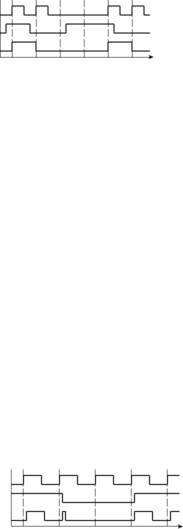
450 CHAPTER TEN design methodology
such components are still affected by clock transitions, even when the
clock-enable input is 0. With clock gating, the components see no clock
transitions when the clock is turned off, as shown in Figure 10.8. Here,
the clock is gated off for two cycles. During that interval, the component
consumes no dynamic power.
Gating a clock is not as simple as inserting an AND gate in the clock
signal. Given the delay in an AND gate, the resulting clock edges would
be skewed from those of the ungated clock, making it difficult to meet
timing constraints. Also, since the gating control signal is typically gener-
ated by a clocked control section, a naive approach can lead to glitches
on the gated clock signal, as shown in Figure 10.9. The glitch may cause
unreliable triggering of the components to which the gate clock is con-
nected. Further, if the control signal has glitches, for example, due to dif-
fering delays in paths through combination logic that generates the signal,
those glitches may be passed through to the gated clock. The solution to
these problems is not to express the clock gating in the RTL model of the
circuit. Rather, we should treat clock gating as a power optimization to be
implemented by clock insertion tools during physical design. Several clock
synthesis tools can perform such power optimization.
As with optimization of other parameters, we need to perform analy-
sis of a circuit design to determine whether power constraints are met
in the final circuit, the actual power consumption will depend on the
clock frequency and on the relative frequency of changes of signal val-
ues, compared to the clock frequency. A power analysis tool can estimate
the circuit’s power consumption based on estimates of those frequencies.
A good way to make such estimates is to monitor the values of signals
during simulation of a model of the circuit. The tool can then combine the
acquired data with power consumption data from the technology library
and load models for the interconnecting signals.
D
clk
Q
FIGURE 10.8 Timing
diagram for a fl ip-fl op with a gated
clock.
gated clk
master clk
control signal
FIGURE 10.9 Glitch on a
gated clock due to poor design.
1. If we need to achieve a major improvement in system performance,
should we focus effort in earlier or later stages of the design fl ow?
2. Why is cost of a chip nonlinearly related to circuit area?
3. How can we affect circuit area during the functional design stage of
the design fl ow?
4. Identify a means of improving system performance that we might
consider in the architecture exploration stage. What trade-offs arise
from improving performance?
5. How does a timing budget help a design team to meet timing
constraints?
6. What is the purpose of specifying timing constraints for synthesis?
7. How does a static timing analyzer verify timing for a synthesized
design and for a placed and routed design?
8. If timing constraints are not met, what must we do?
9. Briefl y describe two techniques for reducing power consumption.
10. Why should clock gating not be implemented in RTL model code?
How is it better implemented?
10.3 DESIGN FOR TEST
The design flow that we have described starts with architecture explo-
ration and proceeds through to delivery of design files for manufacture
of ASICs or programming of FPGAs. Once the chips have been manu-
factured, they must be tested to ensure that they work correctly. There
are several reasons why manufactured chips might not work, including
problems arising during wafer manufacture and during packaging. Some
problems cause whole batches of chips to fail, whereas others produce
isolated failures. The aim of testing after manufacture is to identify the
defective chips so that they can be discarded rather than supplied to cus-
tomers. Ideally, the cause and location of faults can be recorded so that
the manufacturing process can be adjusted to enhance yield.
In the case of ASICs, developing tests for the chip is part of the design
process. In the case of FPGAs, test development is part of the process of
developing the FPGA as an implementation fabric. The FPGA used as
the implementation target of a final design is already tested as part of its
KNOWLEDGE
TEST QUIZ
KNOWLEDGE
TEST QUIZ
10.3 Design for Test CHAPTER TEN 451
452 CHAPTER TEN design methodology
manufacture. However, the FPGA must still be inserted into a PCB as part
of a larger system, which itself must be tested as part of its manufacture.
In many systems, faulty PCBs are not discarded. Instead, defective chips
on the PCBs are replaced, and the repaired PCB retested and returned to
service.
For a simple circuit, testing could involve applying test cases on the
chip inputs and verifying that the chip produces the correct outputs. This is
similar in concept to verification during the design stage. However, rather
than verifying that the design meets functional requirements, the intention
is to verify that the manufactured chip performs as designed. Nonethe-
less, the same question of feasibility arises. As the number of possible
input values and input sequences increases, testing that the chip operates
correctly in all cases becomes infeasible. The time available for testing
is much less than for design verification, since thousands or millions of
chips must be tested individually. Furthermore, testing requires use of test
equipment to physically apply input values and measure output values.
Such equipment is a costly resource, so its use must be minimized.
We can reduce the time and cost involved in testing a system by
including additional circuitry to improve the system’s testability. Such
circuitry includes elements that make internal nodes observable, or that
perform testing automatically as a special mode of system operation. We
use the term design for test (DFT) to refer to design techniques that seek
to improve testability. In the remainder of this section, we will describe
the way in which we can develop test cases specifically aimed at locating
faults. We will then look at two approaches to adding hardware to designs
to improve testability.
10.3.1 FAULT MODELS AND FAULT SIMULATION
As part of the design flow, we need to develop a set of test vectors, or
test patterns, that is, combinations of input values for the circuit that can
be used to expose faults. The idea is that application of each test vector
(or small sequence of test vectors) should cause the circuit to produce a
given output. If the circuit produces a different output, the circuit is faulty.
A good choice of vectors may also be able to locate the fault within the
circuit.
In order to work out how to expose faults, we need to consider the
kinds of faults that can occur in a circuit. We rely on fault models that
are abstractions of the effects produced by faults. We use a fault simulator
that simulates the operation of the circuit with a given fault injected at a
given location. The simulator applies test vectors until an incorrect output
results, indicating that the fault has been detected. If no incorrect output
is produced for all of the test vectors, the fault remains undetected by that
set of vectors. The simulator repeats the simulation for other faults and
other locations in the circuit. Once all of the faults have been simulated,
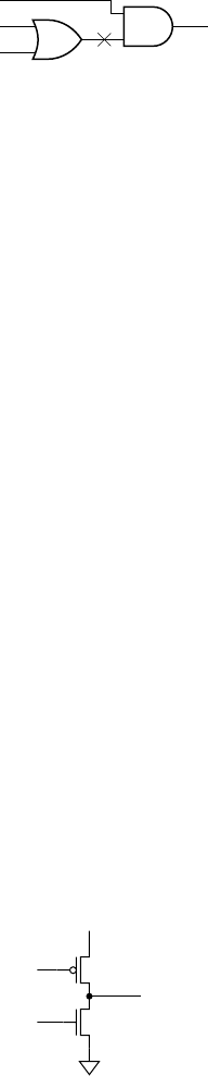
the fault coverage of the test vectors, that is, the proportion of faults
detected, can be determined. Ideally, the fault coverage should be 100%,
but for a large design, this may not be feasible. In choosing the test vec-
tors, we can use an automatic test pattern generator (ATPG), an EDA tool
that analyzes a circuit and seeks to create a minimal set of test vectors
with as close to full coverage as possible.
A simple and commonly used fault model is the stuck-at model, in
which an input or output of a gate in a circuit can be stuck at 0 or stuck at
1, rather than being able to change between 0 and 1. Such a fault might be
caused by a short circuit to the ground or power supply. This is illustrated
in Figure 10.10, in which an input to the AND gate is stuck at 1. For
some input combinations to the circuit (b 1 or c 1), the value at the
stuck node would normally be the same as the stuck-at value; the circuit
would produce the correct output, and we would not detect the fault. For
other input combinations (b 0 and c 0), the value at the stuck node
would be the opposite of the stuck-at value. Whether we could detect the
fault would then depend on the remaining logic between the stuck node
and the circuit’s output. In this circuit, if a 0, the output value is inde-
pendent of the value at the stuck node, so the fault is masked. However,
if a 1, the value of the stuck node is propagated to the output, allowing
us to detect the fault. In general, detecting the fault involves applying
a combination of input values that sensitizes the path from the fault to
the output and that drives the stuck node to the opposite of its stuck-at
value. A node in a circuit is observable if a fault at the node can be made
to result in an incorrect output value. The node is controllable if there are
input combinations that cause the node to take on a given value. Observ-
ability and controllability of nodes in a circuit determine the testability
of the circuit.
Other fault models consider the transistor-level circuits for gates, and
involve transistors being stuck on or stuck off. This allows us to detect
faults that are not adequately represented by the stuck-at fault model. For
example, given the output driving circuit of a gate, shown in Figure 10.11,
a fault might cause the upper transistor to be stuck on. When the gate
should be driving a high logic level, its output is correct. However, when
it should be driving a low logic level, both transistors are on. This creates
a voltage divider, and the output logic level is an invalid level between
the valid high and low levels. How this propagates through the rest of
the circuit depends on the input thresholds of the gates connected to the
driver, and may not be detectable simply by examining the output values.
A testing approach used for such faults is to measure the steady-state
current drawn from the power supply (I
DDQ
) to detect the increase when
both transistors are on. Further fault models include bridging faults, rep-
resenting short-circuit connections between signal wires; delay faults, in
which the propagation delay of a circuit is longer than normal; and faults
in storage elements.
10.3 Design for Test CHAPTER TEN 453
a
1
b
c
z
FIGURE 10.10 A circuit with
a stuck-at-1 fault.
stuck-on
+V
FIGURE 10.11 Output driver
circuit of a gate.
10.3.2 SCAN DESIGN AND BOUNDARY SCAN
In this book, we have described the RTL view of digital systems, consisting
of combinational circuits that transform and transfer data between regis-
ters. The fault models and fault detection techniques that we described in
the preceding section work well for combinational circuits, but are difficult
to adapt to detect faults in registers and other storage elements. The prob-
lems are compounded when the registers are buried deep within a data-
path, since they are significantly more difficult to control and observe.
Scan design techniques address this problem by modifying the registers
to allow them to be chained into a long shift register, called a scan chain, as
shown in Figure 10.12. Test vectors can be shifted into the registers in the
chain, under control of the test mode input, thus making them controllable.
Stored values can also be shifted out of the registers, thus making them
observable. Furthermore, the chain of registers allows us to control and
observe the combinational blocks between registers. We can test each com-
binational block separately. This process consists of shifting test values into
the register chain until the test vector for each block reaches the input reg-
isters for that block. We then run the system in its normal operational mode
for one clock cycle, clocking the output of each block into the block’s out-
put registers. We also need to apply test vectors to the external inputs of the
system and observe the external outputs of the system, in order to test any
combinational input and output circuits. Finally, we shift the result values
out through the register chain. The test equipment controlling the process
compares the output values with the expected results to detect any faults.
This sequence is repeated until all of the test vectors have been applied to
all of the combinational blocks, or until a fault is detected.
This form of design for test has a number of advantages and disad-
vantages. Chief among its advantages is the increased controllability and
observability provided. This makes achieving high fault coverage feasible,
especially for large circuits. We can reduce the test generation problem to
that of testing combinational circuits, which can largely be automated by
D
scan_in
mode
QD
scan_in
mode
QD
scan_in
mode
Q
data_in
scan_in
test_mode
clk
data_out
scan_out
clk clk clk
FIGURE 10.12 Connection
of modifi ed registers in a scan
chain.
454 CHAPTER TEN design methodology
ATPG tools to achieve 100% fault coverage. Moreover, the modification
of the registers to allow them to function as shift registers can also be
automated. One approach is to design and synthesize the circuit normally,
generating a gate-level circuit with flip-flops implementing the registers.
Then as part of physical design, a tool can substitute modified flip-flops
that have a shift mode, as shown in Figure 10.13. The circuit is placed
normally. Finally, during the routing step, connections are made between
adjacent flip-flops to form the shift-register chain. This minimizes the
routing overhead and interference with other signal wires. The DFT tools
can compensate for the resulting placement-dependent ordering of test
vector input and output bits in the scan chain.
The main disadvantage of scan design is the overhead, both in cir-
cuit area and delay. The modified flip-flops have additional circuitry,
including an input multiplexer to select between the normal input
and the output of the previous flip-flop in the scan chain. The area
overhead for scan design has been estimated at between 2% and 10%.
The input multiplexer imposes additional delay in the combinational
path leading to the flip-flop input. If the path is a critical timing path,
performance of the whole system is affected. Another disadvantage of
scan design, when compared to some other DFT techniques, is that
the scan chain is very long. Shifting test vectors in and result vec-
tors out takes a large fraction of test time, so the system cannot be
tested at full operational speed. That overhead time can be reduced
by dividing the scan chain into segments that can be shifted in paral-
lel. However, each chain requires separate input and output pins, so
we must compromise between test-time overhead and test-pin-count
overhead.
One issue to consider in adding hardware to enhance testability is the
possibility of faults within the test hardware. In the case of scan chains,
faults could prevent the flip-flops from operating as shift registers cor-
rectly, and the wiring for the scan chains could be defective. Fortunately,
we can test the scan chain itself quite readily. We simply need to insert a
sequence of 0s and 1s into the chain and shift it through to the output
of the chain. If we see the sequence unchanged at the expected time, we
know the scan chain is defect free. We can then proceed to test the internal
circuits of the system.
D
CE
Q
0
1
D
CE
clk
mode
scan_in
Q
clk
FIGURE 10.13 Modifi ed
fl ip-fl op for use in a scan chain.
10.3 Design for Test
CHAPTER TEN 455
456 CHAPTER TEN design methodology
The concept of scan design can be extended for use in testing the
connections between chips on a PCB, leading to a technique called bound-
ary scan. The idea is to include scan-chain flip-flops on the external pins
of each chip. To test the PCB, the test equipment shifts a test vector into
the scan chain. When the chain is loaded, the vector is driven onto the
external outputs of the chips. The scan-chain flip-flops then sample the
external inputs, and the sampled values are shifted out to the test equip-
ment. The test equipment can then verify that all of the connections
between the chips, including the chip bonding wires, package pins and
PCB traces, are intact. Various test vectors can be used to detect different
kinds of faults, including broken connections, shorts to power or ground
planes, and bridges between connections.
The success of boundary scan techniques led to the formation of the
Joint Test Action Group (JTAG) in the 1980s for standardizing boundary
scan components and protocols. The term JTAG has now become syn-
onymous with boundary scan in its basic and extended forms, supporting
automatic testing of individual chips and PCBs containing multiple chips.
Standardization has been managed for some time by the IEEE as IEEE
Standard 1149.1.
The JTAG standard specifies that each component have a test access
port (TAP), consisting of the following connections:
Test Clock (TCK): provides the clock signal for the test logic.
Test Mode Select Input (TMS): controls test operation.
Test Data Input (TDI): serial input for test data and instructions.
Test Data Output (TDO): serial output for test data and instructions.
There is also an optional Test Reset Input (TRST), but it is not widely
used in practice. Figure 10.14 shows a typical connection of automatic
test equipment (ATE) to the TAPs of components on a PCB. Figure 10.15
shows the test logic within each component. The TAP controller governs
operation of the test logic. There are a number of registers for test data
and instructions, and a chain of boundary scan cells inserted between
external pins and the component core. A typical boundary scan cell is
왘
왘
왘
왘
ATE
TMS
TCK
TDOTDI TDI
TMS
TCK
TDO TDI
TMS
TCK
TDO TDI
TMS
TCK
TDO
FIGURE 10.14 Connection
of ATE to a system with multiple
JTAG TAPs.
shown in Figure 10.16. Depending on the control inputs to the cell, data
can flow straight through, input data can be captured, output data can
be driven, and test data can be shifted through. Input and output pins of
the component each require just one cell. Tristate output pins require two
cells: one to control and observe the data, and the other to control and
observe the output enable. Bidirectional pins require three cells, as they
are a combination of a tristate output and an input.
The TAP Controller operates as a simple finite-state machine, changing
between states depending on the value of the TMS input. Different states
govern shifting of data into the Instruction Register or one of the data
registers (including the scan chain). The JTAG standard defines a number
of instructions formats for operations that select among data registers,
control the mode of the scan chain, and so on. There are also instructions
for component-specific extensions, including built-in self test modes that
we will discuss in Section 10.3.3. The JTAG standard also defines the
Bypass Register
Instruction Decoder
Instruction Register
TAP Controller
Design-specific Registers
Component
Core
TDI
TMS
TCK
TDO
Output
Pins
Tristate
Output
Bidirectional
Output
Input Pins
FIGURE 10.15 Architecture
of a component with JTAG
boundary scan.
0
1
0
1
Mode
UpdateDR
ClockDR
ShiftDR
data_in
scan_in
data_out
scan_out
DQ DQ
clk clk
FIGURE 10.16 A JTAG
boundary scan cell for an input or
output pin.
10.3 Design for Test
CHAPTER TEN 457
458 CHAPTER TEN design methodology
Boundary Scan Description Language (BSDL), which is a subset of VHDL
used to specify the pins, registers, and instructions implemented in the test
logic of a component. We can use a BSDL description of a component,
together with a set of test vectors, as input to ATE for testing the compo-
nent and the board in which it is embedded.
While the boundary scan technique originated as a means of testing
connections between components on a board, the JTAG boundary scan
cells have been designed to allow testing of the component core also. The
cells can be configured to isolate the component core’s inputs from the
package input pins. Test data can be shifted into the cells at the inputs
and then driven onto the core’s inputs. The core’s outputs can be sampled
into the cells at the output pins and then shifted out to the ATE. Thus, the
JTAG architecture solves two problems: in-circuit testing of components
in a system, and in-circuit testing of the connections between the compo-
nents. This flexibility has led to the widespread use of the standard, with
EDA tools available for insertion of test logic into designs during various
stages of the design flow. The JTAG standard has also been extended
to support in-circuit programming of ROMs and configuration of PLDs,
including FPGAs.
10.3.3 BUILT-IN SELF TEST (BIST)
The DFT approaches we have considered so far rely on developing test
vectors during design of a system and applying the vectors to manufac-
tured components to test them. While scan-design and boundary scan
techniques improve testability of components, there is still significant time
overhead in shifting test vectors in and results out of each component.
Furthermore, the components cannot be tested at full operating speed,
since test vectors for each cycle of system operation must be shifted in
over many clock cycles.
We can avoid these problems using built-in self test (BIST) techniques,
which involve adding test circuits that generate test patterns and analyze
output responses. With BIST included in a system, the role of the ATE is
reduced to initiating test operations, verifying successful completion, or, if
a test fails, storing any diagnostic information produced by the BIST cir-
cuits. One of the advantages of BIST is that, being embedded in a system,
it can generate test vectors at full system speed. This significantly reduces
the time taken for test. BIST hardware can also generate multi-cycle test
sequences, making it possible to test for classes of defects that are diffi-
cult to expose with other techniques. The disadvantage, of course, is the
larger area overhead. However, that cost may well be compensated for by
the reduced testing cost. A further advantage is that the BIST hardware
remains available during the operational lifetime of the system, and can
be used for testing when the system is in the field. There are stories told
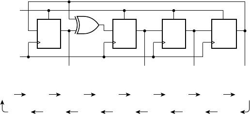
of customers who were unaware of a fault in a system until a service
engineer arrived to repair the system. A system with BIST and redundant
components, capable of reporting faults to a service center over a network
connection, makes such stories plausible.
There are two main aspects to consider when designing a BIST imple-
mentation: how to generate the test patterns, and how to analyze the
output response to determine whether it is correct. The main problem is
to devise circuits for these aspects that are not excessively large and that
do not adversely affect normal system performance.
The most common means of generating test patterns is a pseudo-
random test pattern generator. Unlike true random sequences, pseudo-
random sequences can be repeated from a given starting point, called
the seed. Nonetheless, they have similar statistical properties to true
random sequences. Pseudo-random sequences can be readily generated
with a simple hardware structure called a linear-feedback shift register
(LFSR). Figure 10.17 shows an LFSR for generating sequences of 4-bit
values. The sequence is initiated by presetting the flip-flops, generating
the test value 1111 as the seed. On successive clock cycles, the LFSR
generates values in the sequence shown in Figure 10.17. The sequence
contains all possible 4-bit values except 0000. In most applications, it
is desirable to include that value also. Fortunately, we can modify the
LFSR to form a complete feedback shift register (CFSR), as shown in
Figure 10.18, which generates all possible values. Similar circuits can
be designed to generate pseudo-random test vectors of other lengths.
Placement of the XOR gates within the LFSR is determined by the
characteristic polynomial of the LFSR, referring to the mathematical
theory underlying LFSR operation. Discussion of the theory is beyond
the scope of this book.
Analyzing the output response of a circuit to the test patterns pre-
sents more of a problem. In most cases, it would be infeasible to store
the correct output response for comparison with the circuit’s output
DQ
preset
DQ
preset
DQ
preset
DQ
preset
Q1 Q2 Q3 Q4
preset
clk
1111 1011 1001 1000 0100 0010 0001 1100
0110001111011010010111100111
clk clk clk clk
FIGURE 10.17 A 4-bit LFSR
for generating pseudo-random test
vectors.
10.3 Design for Test
CHAPTER TEN 459
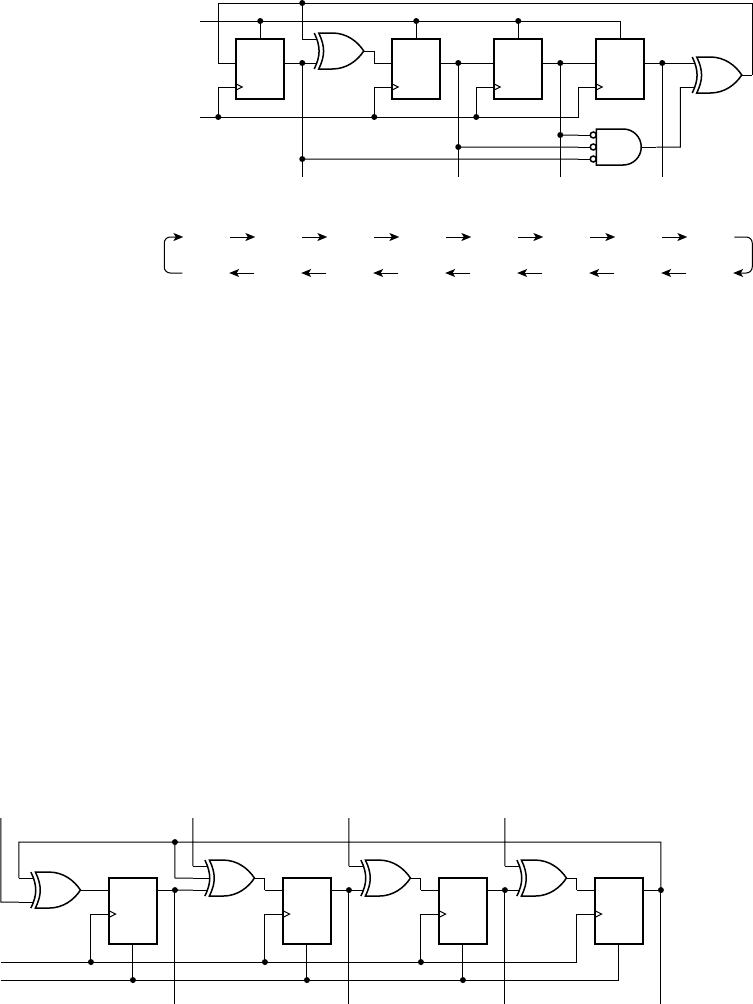
response, since the storage required could well be larger than the circuit
under test. Instead, we need to devise a way of compacting the expected
output response and the circuit’s output response. Doing so requires
less storage, and comparison hardware, though at the cost of circuitry
to compact the circuit’s outputs. There are several schemes for output
response compaction, but the most commonly used is signature analysis.
This technique is closely related to use of LFSRs for test pattern gen-
eration, and the same mathematical theory underlies operation of both.
A signature register forms a summary, called a signature, of a sequence
of output responses. Two sequences that differ slightly are likely to have
different signatures. Figure 10.19 shows an example of a multiple-input
signature register (MISR), with four inputs from a circuit under test and
a 4-bit signature.
Use of BIST using an LFSR for test-pattern generation and a signature
register for response analysis requires us to perform a logic simulation of
the circuit without faults. Since the sequence generated by the LFSR is
determined by the seed, we can perform the simulation with that sequence
DQ
preset
DQ
preset
DQ
preset
DQ
preset
Q1 Q2 Q3 Q4
preset
clk
1111 1011 1001 1000 0100 0010 0001
1100
0000
0110001111011010010111100111
clk clk clk clk
FIGURE 10.18 A 4-bit
CFSR for generating pseudo-
random test vectors.
DQ
Q1
D1 D2 D2 D3
Q2 Q3 Q4
clk
DQ DQ DQ
clear
clk
clear
clk
clear
clk
clear
clk
clear
FIGURE 10.19 A 4-bit MISR
with four inputs from a circuit
under test.
460 CHAPTER TEN design methodology
of input values. We use the output values from the simulation to compute
the expected signature, and save the signature for use during test. When
BIST of a circuit is initiated, either by ATE during manufacturing test or by
an in-system test controller during system operation, the LFSR generates
test patterns and the MISR computes the signature of the actual circuit’s
outputs. The ATE or test controller then shifts the computed signature out
of the MISR and compares it with the expected signature. If they are the
same, no fault is detected (though there is a chance that an actual fault
remains undetected). If they differ, there is definitely a fault.
In this section, we have introduced some of the basic concepts of BIST.
In practice, BIST and design for test techniques have been developed to
much greater sophistication. There is a whole segment of the electronics
design industry devoted to test, with vendors offering a range of software
and test equipment. Design for test techniques sit at the interface between
the design community and test community. In any significant electronics
design project, it is essential that design and test engineers communicate
throughout the design process to ensure that the system will be testable
during manufacture, and, if required, during operation once deployed.
1. What is meant by the term design for test?
2. What does a fault simulator do?
3. Describe the stuck-at fault model, and identify circuit defects that
are represented by the model.
4. What is meant by a circuit node being controllable and observable?
5. How does I
DDQ
testing detect transistor stuck-on faults?
6. What changes must be made to a circuit to create a scan chain?
7. Identify an advantage and a disadvantage of scan design over testing
using external pins only.
8. How does boundary scan enhance testability of PCB-based systems?
9. Identify the signals required in a JTAG test access port.
10. What is the purpose of a JTAG TAP controller in a component?
11. Why does a bidirectional tristate pin require three boundary scan
cells?
12. What circuits are added to a system for built-in self test?
13. Why is BIST useful after manufacturing test of a system?
14. What purposes do LFSRs and MISRs have in signature-based BIST?
KNOWLEDGE
TEST QUIZ
KNOWLEDGE
TEST QUIZ
10.3 Design for Test CHAPTER TEN 461
462 CHAPTER TEN design methodology
10.4 NONTECHNICAL ISSUES
We have now covered all of the technology-related aspects of digital sys-
tem design that we sought to cover in this book. However, they are not the
only aspects we must think about. We finish by discussing a few nontech-
nical issues that bear upon design projects. In some cases, the best techni-
cal choices may not be the best choices when all things are considered.
Electronics products, like most products, go through life cycles.
Product design is just one stage in the life cycle. It is preceded by market
research and financial modeling. After design, manufacturing facilities
and supply channels, and sales and distribution channels need to be estab-
lished. Depending on the product, there may be a need for maintenance
and repair, or for customer service. During the product’s lifetime, it may
be redesigned to meet changing needs, or may be reused in other products.
Finally, the product becomes obsolete and is retired from production and
support.
There are various financial models that can be applied to estimate
revenue from a product over its life cycle. Generally, revenue from a
product typically peaks early in the product’s life cycle, and tails off until
obsolescence. The non-recurring engineering (NRE) costs of developing
the product, along with other up-front costs, must be met from the rev-
enue stream. If the product is aimed at a competitive market, entering
the market early has a critical impact on revenue. Late entry allows com-
petitors to gain market share, reducing the revenue available for the late
product, and possibly making it unprofitable. Hence, time-to-market is an
important nontechnical measure for a design project. For many consumer
products, such as cell phones and media players, product life cycles are
very short, so there is only a short window of opportunity to gain suf-
ficient revenue for profitability. Time-to-market pressures for design of
such products are very intense.
In other industry segments, products have very long life cycles. Exam-
ples are military systems and telecommunications infrastructure. For such
products, attributes such as reliability and maintainability are important.
For example, considerations such as longevity of a vendor company may
override technical considerations in choice of components for a system.
Such long-lived products must typically be supported throughout their
lifetime. Hence, the design phase will involve more than just the techni-
cal design of the circuit. It will also involve development of design docu-
mentation, and liaison with support service providers to develop support
plans, procedures and documents.
Another important factor to consider in design of digital systems is
that the implementation technology continues to evolve rapidly. Each gen-
eration of chip technology allows more transistors to be packed into a
given chip area, more bits of storage per memory chip, and higher clock
frequencies. If the design process for a complex system spans an 18-month
period, a new technology generation is likely to be available when the
product reaches the manufacturing stage. Designing using the previous
generation may well lead to a product with lower performance or capac-
ity than competitors’ products. When we start a design project, we must
be aware of technology trends and make projections to determine the
appropriate technology for the future manufacture of our product.
As we have mentioned throughout this book, design of a digital system
is a complex undertaking. For smaller systems, a small team of engineers
can feasibly deal with product definition and specification, detailed
design, verification, and manufacture. Even so, a systematic methodol-
ogy reduces the risk of the product development project going off the
rails. For larger systems, a larger development team is typically needed.
Different team members bring expertise in different areas to the project.
Indeed, larger teams are often structured with subteams being respon-
sible for different aspects of the design methodology, such as architectural
definition, detailed design, verification, test development, and liaison with
the manufacturing facility. It is important for individual team members to
understand the structure of the overall project and the context in which
they are working. In particular, maintaining good communication and
information flow within the project is critical. Good project management
is essential to a successful outcome.
1. Identify some of the main stages in a product’s life cycle.
2. Why is time-to-market critical for some products?
3. For products with long lifetimes, what additional activities are often
required, beyond technical design of the product?
4. If a system is designed for a competitive market using technology
that is current at the start of the design process, what risk does the
product face?
10.5 IN CONCLUSION
We have now completed our foundational study of digital system design.
We started with the basic elements of digital logic, gates and flip-flops,
and showed how they can be used in circuits that meet given functional
requirements. Given the complexity of requirements for most modern
systems, we appealed to the principle of abstraction as a means of man-
aging complexity. In particular, we use hierarchical composition to build
blocks from the primitive elements, and systems from those blocks. By
this means, we were able to reach the level of complete embedded systems,
comprising processors, memories, I/O controllers, and accelerators, with-
out becoming overwhelmed by the detailed interactions of the millions of
KNOWLEDGE
TEST QUIZ
KNOWLEDGE
TEST QUIZ
10.5 In Conclusion CHAPTER TEN 463
464 CHAPTER TEN design methodology
transistors involved. Throughout our study, we also paid attention to the
real-world effects that arise in digital circuits and the constraints that they
imply. We showed how a disciplined design methodology helps us meet
functional requirements while satisfying constraints.
The study of digital systems in this book serves as a foundation for
further studies in several areas. On the hardware side, VLSI design involves
study of techniques for design of circuit elements and systems on silicon
integrated circuits, typically starting with CMOS digital circuits, but
then extending to analog, radio frequency (RF) and mixed analog/ digital
systems. Also, micro-electromechanical systems (MEMS) and microflu-
idics are becoming increasingly important, particularly for the interface
between digital systems and the real world. At the interface between hard-
ware and software, digital design leads to studies in computer organiza-
tion and computer architecture, since a computer is just a specialized kind
of digital system. Embedded systems design also lies on this interface,
since the trade-off between hardware and software implementation is an
important aspect. On the software side, studies in operating systems and
compiler design benefit from an understanding of how computer hard-
ware functions. Finally, the electronic design automation tools themselves
make an interesting topic for advanced study, and are key to successful
digital system design methodologies.
The integrated circuit technology on which digital systems are based
has been continually developing since its inception. Moore’s Law charac-
terizes the development, describing how the number of transistors avail-
able on an IC increases exponentially. This rule has held solidly since the
1960s until now, despite several predictions during that time that one
road block or another would halt progress. The semiconductor industry
still holds to Moore’s Law, with the International Technology Roadmap
for Semiconductors (see www.itrs.net) mapping out several future gen-
erations of IC technology over the next fifteen years. Feature sizes for
leading-edge processes are projected to be reduced from 65nm in 2007,
through 45nm, 32nm, and 22nm, down to 16nm in 2019. Making use of
the enormous number of transistors that will be available (and that will
be required on a chip to make fabrication economically viable) will be
one of the main challenges facing designers. Many commentators predict
that ASICs will become increasingly uneconomical for all but the largest-
volume applications. Instead, customizable platforms targeted at vari-
ous classes of applications will become more common. Most designs will
involve customization of such platforms, either through programmable
fabric embedded in the platform, or through customization of the final
layers of metal wiring on the chip. Of course, the further into the future
we look, the harder it is to predict, as alternative evolutions diverge and
the probability of some disruptive new technology emerging increases.
Whatever happens, digital systems design promises to remain an exciting
endeavor.

10.6 CHAPTER SUMMARY
A design methodology codifies the process of design, verification
and preparation for manufacture of a product. It involves develop-
ment of virtual prototypes to support design analysis and refinement.
Architecture exploration is the process of modeling and evaluat-
ing candidate designs at a high level of abstraction. A system is
partitioned for subsequent refinement. Logical partitioning identi-
fies functional components, whereas physical partitioning identifies
physical hardware components. Logical functions are mapped onto
physical partitions.
Functional design refines partitions to a level from which imple-
mentations can be synthesized. Components may be implemented
through IP reuse or by core generators.
Functional verification ensures that the refined design meets func-
tional requirements, and can be performed using simulation and
formal verification. Functional coverage is the proportion of func-
tionality verified.
Hardware/software co-verification uses instruction-set simulators
and hardware emulation to test software before hardware models
are available. Software and hardware can be tested together using
cosimulation.
An RTL synthesis tool refines HDL models to gate-level circuits com-
posed of components from a technology library, subject to timing
and area constraints.
Physical design involves floorplanning to arrange the blocks of a
circuit, and placement and routing of the gate-level cells.
A design can be optimized at various stages in the design flow. The
main parameters we seek to optimize are area, timing, and power
consumption. This usually involves making trade-offs.
Design for test enhances testability of a product, thus reducing test
cost. Testing involves applying test patterns to a circuit’s inputs and
verifying that the expected outputs are produced.
Fault models represent the effects of defects in a circuit, and are
used by a fault simulator to determine fault coverage of a set of test
vectors.
Testability of a circuit can be enhanced by adding test hardware.
Scan design involves modifying registers to form shift registers for
왘
왘
왘
왘
왘
왘
왘
왘
왘
왘
왘
10.6 Chapter Summary CHAPTER TEN 465

466 CHAPTER TEN design methodology
shifting test vectors into a circuit and output results out. Boundary
scan, including that specified by the JTAG standard, supports
in-circuit testing of components and PCBs.
Built-in self test (BIST) adds autonomous test circuits to components
for use in manufacturing and in-field testing.
Various nontechnical issues affect the design process, including busi-
ness and life-cycle considerations.
10.7 FURTHER READING
The ASIC Handbook, Nigel Horspool and Peter Gorman, Prentice
Hall PTR, 2001. A detailed description of a design flow for ASICs,
including discussion of both technical and nontechnical aspects.
Application-Specific Integrated Circuits, Michael John Sebastian Smith,
Addison-Wesley Professional, 1997 (see also http://www-ee.eng
.hawaii.edu/%7Emsmith/ASICs/HTML/ASICs.htm). A description
of ASIC technology and design methodology.
Surviving the SOC Revolution: A Guide to Platform-Based Design,
Henry Chang et al., Kluwer Academic Publishers, 1999. Deals with
the basic principles of a design methodology addressing a platform-
based approach to the design of embedded systems.
Winning the SoC Revolution, Grant Martin and Henry Chang (editors),
Kluwer/Springer, 2003. A followup to Surviving the SOC Revolu-
tion, including several case studies of design methodologies used for
real commercial projects. Also includes a discussion of nontechnical
aspects of design.
Handbook on Electronic Design Automation of Integrated Circuits,
Louis Scheffer, Luciano Lavagno, and Grant Martin (Editors), CRC,
2006. A comprehensive overview of the design automation algo-
rithms, tools, and methodologies used to design integrated circuits.
Reuse Methodology Manual for System-On-A-Chip Designs, 3rd Edi-
tion, Michael Keating, Russell John Rickford, and Pierre Bricaud,
Springer, 2006. Describes a design methodology for creating reusable
ASIC designs.
Comprehensive Functional Verification: The Complete Industry
Cycle, Bruce Wile, John C. Goss, and Wolfgang Roesner, Morgan
Kaufmann Publishers, 2005. A detailed treatment of functional veri-
fication strategies and techniques and their place in the design flow.
왘
왘

Writing Testbenches Using SystemVerilog, Janick Bergeron, Springer,
2006. Presents many of the functional verification features that
were added to the Verilog language as part of SystemVerilog, and
shows how they are used in the verification process.
Verification Methodology Manual for SystemVerilog, Janick Bergeron,
Eduard Cerny, Alan Hunter, and Andy Nightingale, Springer, 2005.
Describes a methodology for verification of complex digital systems
using a layered approach.
UML for SoC Design, Grant Martin and Wolfgang Müller (editors),
Springer, 2005. A collection of the main contributors of the UML
and SoC workshop at the 2004 Design Automation Conference,
presenting approaches to executable UML, UML translations for
FPGA synthesis and SystemC simulation, as well as UML-specific
SoC methodologies.
A Practical Introduction to PSL, Cindy Eisner, Dana Fisman, Springer,
2006. Describes the Property Specification Language PSL, including
its use for simulation-based and formal verification, and touches on
methodological issues.
The e-Hardware Verification Language, Sasan Iman, Sunita Joshi,
Springer, 2004. Provides a detailed coverage of the e-hardware veri-
fication language (HVL), and its use in implementing a verification
environment.
The Art of Verification with Vera, Faisal Haque, Jonathan Michelson,
Khizar Khan, Verification Central, 2001. Covers the elements of the
Vera testbench tool and the OpenVera language using examples to
show how they can be used to verify different types of designs.
Assertion-Based Design, Harry D. Foster, Adam C. Krolnik, and David
J. Lacey, Springer, 2004. Describes an approach to design that
facilitates verification, based on assertions expressed using the Open
Verification Library (OVL), Property Specification Language (PSL),
and SystemVerilog.
A Designer’s Guide to Built-In Self Test, Charles E. Stroud, Kluwer
Academic Publishers, 2002. A comprehensive reference on the
theory and practice of BIST, including fault models, test pattern
generation, signature analysis, and scan-based design.
10.7 Further Reading CHAPTER TEN 467
This page intentionally left blank
appendix a
knowledge test quiz
answers
ANSWERS FOR CHAPTER 1
section 1.2
1. The two values used in binary representation are 0 and 1.
2. If one input is 0 and the other is 1, the output is 0. If both inputs are 0, the
output is 0. If both inputs are 1, the output is 1.
3. If one input is 0 and the other is 1, the output is 1. If both inputs are 0, the
output is 0. If both inputs are 1, the output is 1.
4. A multiplexer selects between two inputs, based on the value of a select
input. The output value is the same as the selected input value.
5. The outputs of a combinational circuit depend only on the current values of
the inputs, whereas the outputs of a sequential circuit depend on the current
and past values of inputs.
6. A flip-flop stores one bit of information.
7. The term rising edge refers to a transition of a clock signal from 0 to 1.
The term falling edge refers to a transiti
on from 1 to 0.
section 1.3
1. The TTL output voltage levels are 0.4V maximum for logic low and 2.4V
minimum for logic high. The input threshold voltages are 0.8V minimum
for logic low and 2.0V maximum for logic high. The noise margins are 0.4V
for both logic low and logic high.
2. The term fanout refers to the number of inputs driven by a given output.
3. The propagation delay of a component is the time for a change of logic level
at an input to cause a corresponding change at the output.
4. Minimizing the fanout of a component reduces the capacitive loading on the
output, thus reducing the propagation delay.
469
5. Yes, wires do contribute to delay in a circuit, since it takes a nonzero
amount of time for a signal change to propagate along the wire from an
output to an input.
6. The setup time is the interval for which a value to be stored must be present
on the data input before a rising clock edge. The hold time is the interval
for which the value must remain unchanged after the rising clock edge. The
clock-to-output time is the interval from a rising clock edge until the stored
data appears at the output.
7. Static power consumption arises from leakage current flowing through
transistors that are turned off. Dynamic power consumption arises from the
charging and discharging of load capacitance when outputs switch between
logi
c levels.
8. No, the cost of an IC is disproportionately dependent on area.
section 1.4
1. A Verilog module defines the inputs and output of a circuit and the
implementation of the circuit.
2. For each port, the module specifies the name and whether the port is an
input to the module or an output from the module.
3. A structural model is one that describes a circuit as a collection of
interconnected components. A behavioral model is one that describes the
function performed by the circuit.
4. Functional verification involves ensuring that the design performs the
required function. Timing verification involves ensuring that the design
meets its timing constraints.
5. One approach i
s to interpret the model as an executable program using a
simulator. Another approach is formal verification, in which properties of
the design are proven mathematically.
6. Synthesis involves automatic refinement of a model at a higher level of
abstraction into a structural model at a lower level of abstraction.
section 1.5
1. A design methodology is the systematic process of design, verification and
preparation for manufacture of a product. A design methodology specifies
the tasks undertaken, the information required and produced by each task,
the relationships between the tasks, including dependencies and sequencing,
and the CAD tools used.
2. A design methodology makes the design process more reliable and
predictable, thus reducing risk and cost.
470 APPENDIX A knowledge test quiz answers

3. We must revisit a previous task to correct the error.
4. Top-down design involves developing an overall organization of a digital
system to meet requirements, then designing and verifying each of the
subsystems and sub-subsystems, and finally integrating and verifying the
entire system.
5. Two implementation fabrics are field-programmable gate arrays (FPGAs)
and application-specific integrated circuits (ASICs).
6. An embedded system is a digital system in which one or more computers are
embedded as part of the circuit and programmed to implement part of the
required functionality.
7. Hardware/software codesign refers to the practice of des
igning the hardware
and the software of an embedded system together.
ANSWERS FOR CHAPTER 2
section 2.1
1. The truth table for a ·
_
b
_
c is
abc
a ·
_
b
_
c
000 1
001 0
010 1
011 0
100 1
101 1
110 1
111 0
2. Truth tables for the two expressions are
ab a · b
_
a
_
b
00 1 1
01 1 1
10 1 1
11 0 0
APPENDIX A 471

Since the expressions have the same value for all combinations of values for
a and b, the expressions are equivalent.
3. An expression is in sum-of-products form if it is the logical OR of a number
of logical AND terms of variables or negations of variables.
4. The truth table for the AND-OR-Invert gate is
abcd
a · b c · d
0000 1
0001 1
0010 1
0011 0
0100 1
0101 1
0110 1
0111 0
1000 1
1001 1
1010 1
1011 0
1100 0
1101 0
1110 0
1111 0
5. Buffers are used to reduce the load on an output that must be connected to
many inputs.
6. A compacted truth table is
abc f
1
0–– 0
10– 0
110 1
111 0
472 APPENDIX A knowledge test quiz answers

7. The benefit is that it gives us more scope for optimizing the circuit. We
might be able to identify two candidate circuits that both produce the
required outputs for the combinations we do care about, but that differ in
their output for the “don’t care” combinations. If one of the candidates
better meets constraints than the other, we would choose it, accepting
whatever result it yields for the “don’t care” combinations.
8. The dual is
____
a ( b c) (
_
a
_
b) (
_
a
_
c). We need to pay attention to the order
of application of operators when forming the dual.
9. assign f = (a & ~b) | ~c;
10. We should allow a CAD tool to synthesize and optimize a circuit based on
constraints and our chosen implementation fabric, since a CAD tool can
generally do a better job than we could do manually.
section 2.2
1. A 5-bit code can have up to 2
5
32 code words.
2. The minimum number of bits needed is
é
log
2
12
ù
4 bits.
3. There are seven values to represent, so we need a 7-bit one-hot code.
A possible code is Monday: (1, 0, 0, 0, 0, 0, 0), Tuesday: (0, 1, 0, 0, 0, 0, 0),
Wednesday: (0, 0, 1, 0, 0, 0, 0), Thursday: (0, 0, 0, 1, 0, 0, 0),
Friday: (0, 0, 0, 0, 1, 0, 0), Saturday: (0, 0, 0, 0, 0, 1, 0), Sunday:
(0, 0, 0, 0, 0, 0, 1).
4.
wire [0:7] w;
Alternatively, we could use a descending index range:
wire [7:0] w;
5. assign w = 8'b00000000;
6. A single bit flip in a one-hot code always produces an invalid code. If a 0 bit
flips to 1, the resulting word has two 1 bits, which is invalid for a one-hot
code. If the single 1 bit flips to 0, the resulting word has no 1 bits, which is
also invalid.
7. Every valid code word in the augmented code has an odd number of 1 bits.
If a bit flip changes a 0 to a 1, the result has an additional 1 bit, giving an
even number of 1 bits. Similarly, if a bit flip changes a 1 to a 0, the result
has one fewer 1 bits, again giving an even number of 1 bits. In either case,
the error can be detected by testing whether there is an even number of
1 bits.
APPENDIX A 473
8. No, parity cannot be used to correct a bit flip. While we can determine that
a bit has flipped, we cannot determine which bit has flipped. So we cannot
determine the original uncorrupted code word.
section 2.3
1. y
4
a
2
_
a
1
_
a
0
2. intruder_zone[2] == 0, intruder_zone[1] == 1, intruder_zone[0] == 1.
This is the code 011, which represents Zone 4. Thus the output would be
incorrect.
3. We would not be able to distinguish the case of an intrusion being detected
in Zone 1 from the case of no intrusion being detected.
4. It ranks the inputs in priority order. If a given input is 1 and no higher
priority inputs are 1, the encoder outputs the code corresponding to the
given input, regardless of whether any lower priority inputs are 1.
5. The BCD code 0101 represents the decimal digit 5.
6. The 7-segment code corresponding to the BCD code 0011 is 1001111
(the digit 3).
7. A multiplexer allows us to select among two or more data inputs. The value
of the output is the same as the value of the selected input. The selection is
determi
ned by a separate select input.
8. We need to encode the choice of which input to select. Since there are 6
possible choices, we need
é
log
2
6
ù
3 select input bits.
9. We can use five single-bit-wide 2-to-1 multiplexers. Each multiplexer
chooses between the corresponding bits of the encoded data inputs. The
select input is connected in common.
10. The signal would be at a high logic level, indicating falsehood of the
statement “the door is closed.”
11. To turn the motor on, we need to assign a low logic level, represented in
Verilog by the value
0.
section 2.4
1. The purpose of a testbench model is to provide input values to the design
under verification (DUV) and to check that the output values are correct.
2. #1
s = 4'b0101;
3. After executing the last statement, the always block waits for another
occurrence of the event described in its sensitivity list.
474 APPENDIX A knowledge test quiz answers

4. The outputs of the design under verification would not have responded
to the change at the inputs. Instead, they would still reflect the output
generated in response to the previous input values.
5. If the circuit is very simple, comprising just one or two gates, it may be
appropriate to implement it using discrete gates in individual packages. An
example is a circuit that deals with minor differences in signals connecting
off-the-shelf ICs.
6. A PLD is a programmable logic device, that is, a circuit containing some
number of gates whose interconnections can be programmed.
ANSWERS FOR CHAPTER 3
section 3.1
1. A number x is represented using n bits x
n1
, x
n2
, . . . , x
0
, with
x x
n 1
2
n 1
x
n 2
2
n 2
· · x
0
2
0
2. An n-bit unsigned binary number can represent values from 0 to 2
n
1.
3. Since 8191 2
13
1, we need 13 bits in the vector for x. The declaration is
wire [12:0] x;
4. In octal: 01 011 101 ⇒ 135
8
. In hexadecimal: 0101 1101 ⇒ 5D
16
.
5. 10010011 ⇒ 000010010011. The 12-bit result represents the same value as
the original.
10010011 ⇒ 010011. The 6-bit result does not represent the same value,
since a significant 1 bit was truncated.
6.
01001010
10101010
01100000
010000000
The addition does not overflow, since the carry bit out of the most
significant position is 0.
7. In a ripple-carry adder, the carry bit into each position is determined using
the carry bit from the next less significant position. Thus, in the worst case,
carries must propagate through all bit positions of the adder before the final
result is determined. In a carry-lookahead adder, the carry bit into each
position is determined using just the operand bits and the carry bit into the
APPENDIX A 475

adder. Thus, the delay before the final result is determined is less than the
worst-case delay of the ripple-carry adder.
8. We can assign to the concatenation of the carry and result nets, relying on
Verilog’s implicit extension of the operands to yield the carry bit:
assign {c_out, s3} = s1 + s2;
9.
01001010
11101010
0– 1100000
111000000
The subtraction does underflow, since the borrow bit out of the
most-significant position is 1.
10. Use the control signal to complement the second operand by passing each
operand bit through an XOR gate with the control signal as the other gate
input. Also, connect the control signal to the carry input of the adder.
11.
assign smaller = a < b;
12. Since 16 2
4
, multiply by performing a logical shift left by four places; that
is, shift the bits of the number left by four places and append four 0 bits on
the right. Divide by 16 by performing a logical shift right by four places;
that is, shift the bits of the number four places to the right, truncating the
four right-most bits and appending four 0 bits on the left.
13. The product of two n-bit unsigned binary numbers requires 2n bits.
14. Gray codes are often used to avoid incorrect position values arising when
multiple bits of a code change at once. In a Gray code, only one bit changes
between adjacent code words.
section 3.2
1. The weight of the left-most bit is negative (2
n 1
) for 2s-complement
representation, whereas it is positive (2
n 1
) for unsigned
representation.
2. The range of values is 2
11
to 2
11
1, that is, 2048 to 2047.
3. Since 512 2
9
, we need 10 bits in the vector for the number. The
declaration is
wire signed [9:0] x;
476 APPENDIX A knowledge test quiz answers

4. 01110001 ⇒ 000001110001. The 12-bit result represents the same value as
the original.
01110001 ⇒ 110001. The 6-bit result does not represent the same value,
since the truncated bits are different from the resulting sign bit.
11110011 ⇒ 111111110011. The 12-bit result represents the same value as
the original.
11110011 ⇒ 110011. The 6-bit result represents the same value as the
original, since the truncated bits are the same as the resulting sign bit.
5.
_____
11110010 1 00001101 1 00001110.
6. The operand to be subtracted is complemented before being input to the
adder, and the carry input of the adder is set to 1.
7. Since 16 2
4
, multiply by performing a logical shift left by four places;
that is, shift the bits of the number left by four places and append four 0
bits on the right. Divide by 16 by performing an arithmetic shift right by
four places; that is, shift the bits of the number four places to the right,
truncating the four rightmost bits and replicating the original sign bit four
times on the left.
section 3.3
1. The number x is represented by the bits x
m1
, . . . , x
0
, x
1
, . . . , x
f
as:
x x
m 1
2
m 1
. . .
x
0
2
0
x
1
2
1
. . .
x
f
2
f
2. The range is 2
m 1
to 2
m 1
2
f
.
3. We need 9 pre-binary-point bits and 4 post-binary-point bits. So the
declaration is
wire [8:-4] x;
4. assign s3 = s1 – s2;
5. The product requires 28 bits: 10 pre-binary-point bits and 18 post-
binary-point bits.
section 3.4
1. 4.5
10
100.1
2
1.001
2
2
2
. The exponent is represented as
2 2
4
1 17, that is 10001. The mantissa is represented using just the
post-binary-point bits. The number is positive, so the sign bit is 0. The
floating-point representation is 010001001000000000.
APPENDIX A 477
2. 0000000000000000 represents 0.0.
0111100000000000 represents Infinity.
0100010000000000 has a biased exponent of 8, so the actual exponent is
8 1 2
3
1. The number is 1.1
2
2
1
11
2
3.
3. We require the exponent size e to be the smallest such that 2
2
e 1
100;
that is 2
e 1
7, or e 4. For 4 decimal digits of precision, we need at least
4/0.3 14 mantissa bits.
ANSWERS FOR CHAPTER 4
section 4.1
1. The always block responds to a rising edge of the clock. On a rising edge,
the block copies the value of the data input to the data output.
always @(posedge clk)
q <= d;
2. We call such an arrangement a pipeline.
3. The clock-enable input controls when the register updates the stored value.
The register only updates the stored value when the
CE input is 1 at the time
of a rising clock edge. If the
CE input is 0 on a rising clock edge, the register
maintains the stored value unchanged.
4. When an asynchronous reset becomes 1, the flip-flop or register is reset to
zero immediately, whereas a synchronous reset is only acted upon at the
time of a clock edge.
5. A shift register allows the stored data to be shifted by one position.
6. The term “transparent” refers to the fact that data is transmitted through
to the output while the latch-enable input is 1.
7. The implication is that the output is to maintain its previous value,
requiring a latch in the hardware. Thus, the circuit is sequential, not
combinational.
section 4.2
1.
DQ+1 Q
clk
clk
2. The maximum count value is 2
n
1. After that, the counter advances to 0.
478 APPENDIX A knowledge test quiz answers
3. The terminal count, k 1, is decoded and fed back to the synchronous reset.
Thus, the counter advances from k 1 to 0.
4. A decade counter is a modulo 10 counter. It counts from 0 up to 9 and then
advances to 0.
5. An interval timer is a counter whose clock input is a periodic signal with
period t. The counter is loaded with a value k. The terminal count is
reached after an interval of k t. The terminal-count output signal is used
to trigger an activity after expiration of the time interval.
6. The accumulated delay may exceed the clock period. In that case, there will
be clock cycles during which the counter outputs don’t reach the correct
value before the end of the cycle.
section 4.3
1. The datapath contains the combinational circuits that implement the
basic operations required of the digital system and the registers that store
intermediate results.
2. The control section performs control sequencing, that is, ensuring that the
datapath performs the required operations in the right order and at the right
times.
3. Control signals govern the operation of the datapath elements: selecting
operations to be performed and enabling registers. Status signals indicate
whether certain conditions of interest are true, for example, whether data
has certain values, or whether input data is available.
4. In a Mealy finite-state machine, the output function depends on both the
current state and the values of the
inputs. If the input values change during
a clock cycle, the output values may change as a consequence. In a Moore
finite-state machine, on the other hand, the output function depends only on
the current state, and not on the input values.
5.
parameter s0 = 2'b00, s1 = 2'b01, s2 = 2'b10, s3 = 2'b11;
6. Mealy-style output labels are attached to the arcs. Moore-style output labels
are attached to the state bubbles.
section 4.4
1. “Register transfer level” refers to a level of abstraction in our view of a
digital system, in which we focus on transfer of data between registers
through combinational subcircuits.
2. t
co
t
pd
t
su
< t
c
.
3. The critical path is the path from register output to register input with the
longest propagation delay.
APPENDIX A 479
4. The critical path delay determines the shortest clock cycle time for the
system. Since all operations are performed in times determined by the clock,
the critical path determines the overall system performance.
5. We need to focus optimization effort on the critical path or paths to reduce
their delay.
6. Clock skew refers to a situation where a clock edge arrives at different
registers at different times, due to different wire delays in the wires that
distribute the clock signal.
7. Use of registered inputs and outputs avoids the need for a clock period
to accommodate both combinational subcircuit delays and delays though
external pins and wiring.
8. Changes on asynchronous inputs around the ti
me of a clock edge can induce
metastability in input registers.
9. We must debounce an input from a switch to avoid spurious activation of
the system’s response to switch movements.
10. Whereas a combinational testbench simply applies each test case and check
for the correct result, a sequential testbench must synchronize comparison
of results with application of test cases. It must ensure that correct results
occur at the correct times and in the correct order, and that no spurious
results occur at other times.
11. Rather than having a single global clock signal for the entire chip or system,
instead, the system is divided into several regions, each with its own local
clock. Where signals connect from one region to another, they are treated as
asynchronous inputs.
ANSWERS FOR CHAPTER 5
section 5.1
1. The capacity of the memory is 4096 24 98,304 bits. The memory
requires log
2
4096 12 address bits.
2. The effect of a write operation is for the memory to write data present
on the data inputs at the location whose address is present on the address
inputs. The effect of a read operation is for the memory to read the content
of the location whose address is present on the address inputs and drive the
data value on the data outputs.
3. We would connect the address and control signals in common, and connect
the data inputs and outputs of each component to separate groups of four
data input and output signals, as shown in Figure A.1.
480 APPENDIX A knowledge test quiz answers
FIGURE A.1
a(27…0)
en
wr
d_in(3…0)
d_out(3…0)
a(27…0)
en
wr
d_in(3…0)
d_out(3…0)
d_out(7…4)
d_out(3…0)
d_in(7…4)
d_in(3…0)
a(27…0)
en
wr
d_in(3…0)
d_out(3…0)
a(27…0)
en
wr
d_in(3…0)
d_out(3…0)
d_out(15…12)
d_out(11…8)
d_in(15…12)
d_in(11…8)
a(27…0)
en
wr
4. We would use a 2-to-4 decoder to decode two address bits to select
a memory, and a 4-to-1 multiplexer for the data outputs, shown in
Figure A.2.
d_out(7…0)
d_in(7…0)
a(27…0)
a(29…28)
en
wr
0
1
2
3
0
en
1
2
3
a(27…0)
en
wr
d_in(7…0)
d_out(7…0)
a(27…0)
en
wr
d_in(7…0)
d_out(7…0)
a(27…0)
en
wr
d_in(7…0)
d_out(7…0)
a(27…0)
en
wr
d_in(7…0)
d_out(7…0)
FIGURE A.2
APPENDIX A 481
5. The location would reside in component 0.
6. The states of a tristate driver are logic low, logic high and high impedance.
7. We can omit the output multiplexer and simply connect the data outputs of
the memory components together. Moreover, the separate data inputs and
outputs can be combined into bidirectional data connections.
section 5.2
1. A RAM can perform both write and read operations, whereas a ROM can
perform read operations only. The data in a ROM must either be placed in
the memory when the device is manufactured or be programmed into the
device after manufacture.
2. A volatile memory requires power to maintain the stored data and loses
data if power is removed. A nonvolatile memory, on the other hand,
maintains the stored data while power is removed.
3. In a static RAM, the stored data persists indefinitely so long as power is
applied to the memory component. In a dynamic RAM, on the other hand,
data decays unless it is periodically refreshed by being read and rewritten.
4. The access time of a RAM is the delay from the start of a read operation to
having valid data at the outputs.
5. The need to set up and hold address and data values before and after
activation of the control signals and to keep the values stable duri
ng the
entire cycle means that we must either perform operations over multiple clock
cycles, or use delay elements to ensure correct timing within a clock cycle.
6. Flow-through SSRAMs have registers on the inputs, but not on the data
outputs. Pipelined SSRAMs, on the other hand, have registers both on the
inputs and on the data outputs.
7. Memory storage is represented by an array variable. Each array element
represents a storage location.
8. A multiport memory can perform multiple memory access operations at
the same time, giving a higher overall access rate, and allowing separate
subsystems to access the memory independently without contention.
9. We should consult the data sheet for the memory component to understand
the effect.
10. FIFO stands for “first-in, first-out,” and refers to the order in which data is
written to and read from the memory.
11. A FIFO allows us to smooth out the flow of data between the domains. Data
arriving is written into the FIFO synchronously with the sendi
ng domain’s
clock, and the receiving domain reads data synchronously with its clock.
482 APPENDIX A knowledge test quiz answers
section 5.3
1. Soft errors are transient, and involve a bit flip in a memory cell without a
permanent effect on the cell’s capacity to store data. Hard errors persist in a
memory circuit. A memory cell or chip affected by a hard error is no longer
able to store data.
2. In DRAMs, soft errors are typically caused by high-energy neutrons
generated by collision of cosmic rays with atoms in the earth’s atmosphere.
The neutrons collide with silicon atoms in the DRAM chip, leaving a stream
of charge that can disrupt the storage or reading of charge in a DRAM cell.
3. We are not able to take any action to correct the data, since parity does not
allow us to identify which bit flipped causing the parity error.
4. Single-error correction and double-error detection of 4-bit data words
requi
res log
2
4 2 4 check bits per word.
ANSWERS FOR CHAPTER 6
section 6.1
1. Photolithography is the use of a photographic process to draw on the
surface to control which areas are affected by processing steps.
2. The larger the IC area, the greater the IC cost. The higher the defect density,
the greater the cost, since defective ICs must be discarded and their cost
amortized over the remaining good ICs.
3. “L” stands for low power, and “S” refers to the use of Schottky diodes to
reduce switching delays.
4. The term glue logic refers to simple logic circuits for interconnecting LSI
components.
5. ASIC stands for application-specific integrated circuit, and ASSP stands for
application-specific standard product.
6. It would probably not make sense to design an ASIC for a customized
system, since the production volume would be very low. The high NRE
cost would be amortized over a small number of units, making the uni
t
cost excessive. It would probably be better to develop an FPGA-based
design.
7. It would most likely make sense to develop an ASIC for an engine control
system, since the production volume would be very high. The ASIC
would have lower manufacturing cost per unit than a programmable part.
Amortizing the NRE for the ASIC over the large production run would
result in a lower overall cost per unit than that for the FPGA.
APPENDIX A 483
section 6.2
1. Whereas the function performed by a fixed-function component is
determined by the logic circuit for the component, the function of a
programmable logic device can be programmed after manufacture.
2. A fuse map is a file used by a programming instrument to determine which
fuses to blow in a programmable array logic (PAL) device.
3. Output
O8 implements the function
______
I2
__
IO2 I10 , with the output enabled
by the condition
l9.
4. The state bit
S2 would be stored in the flip-flop. The 4-to-1 multiplexer
would select input 3, taking the negated value of
S2 from the flip-flop and
negating it again to present
S2 at the output. The 2-to-1 multiplexer would
select input 0, feeding the negated value of
S2 back to the AND array. The
buffer/inverter provides both
S2 and its negated form to the array.
5. The system can be upgraded after delivery by storing new configuration
information, rather than having to replace chips or other hardware.
6. The logic blocks can be programmed to implement simple combinational
or sequential logic functions. The I/O blocks can be programmed to be
registered or nonregistered, as well as implementing various specifications
for voltage levels, loading and timing.
7. FPGAs also contain embedded RAM blocks and a programmable
interconnection network. The more recent FPGAs also include special
circuits for clock generation and distribution.
8. The configuration needs to be stored in a separate nonvolatile memory, and
additional ci
rcuits need to be included in the system to manage loading the
configuration.
9. An antifuse is a conductive connection that is formed during programming,
as opposed to being blown.
10. A platform FGPA serves as a complete platform upon which a complex
application can be implemented. It includes specialized circuitry such as
one or more processor cores, computer network transmitter/receivers and
arithmetic circuits. In contrast, a simple FPGA includes only basic logic
blocks, embedded memory and I/O blocks.
section 6.3
1. In flip-chip packaging, the connection pads on the IC are covered in
conductive material forming bumps. The IC is flipped over and affixed to
the substrate of the package, with the bumps in direct contact with substrate
connection points. The connection points lead to the external pins of the
package. In contrast, previous packaging involved placing the IC circuit-side
484 APPENDIX A knowledge test quiz answers
up in a package cavity, and joining bond wires from the IC’s connection
points to the lead frame in the package.
2. Insertion-type packages have pins that are designed to be inserted through
plated holes in a printed circuit board (PCB). Solder is melted into the
holes to form electrical connections between the pins and the PCB wiring.
In contrast, surface-mount packages have pins or connection points
that come into contact with a metal pad on the PCB. Solder paste is
applied between each pin and pad and subsequently melted, forming the
connection.
3. Vias are small holes drilled through the layers of a PCB and coated with
metal to form connections between the layers.
4. A ball-grid array (BGA) package would mose likely be used.
section 6.4
1. The term signal integrity refers to the degree to which distortion and noise
effects upon a signal path are minimized.
2. A signal propagates at approximately 150mm per nanosecond along a
typical PCB trace.
3. Ground bounce arises when one or more output drivers switch logic levels.
During switching, both of the transistors in the driver’s output stage are
momentarily on, and transient current flows from the power supply to
ground. The inductance in both the power and the ground connections
causes voltage spikes in the power supply and ground on the IC.
4. Bypass capacitors should be placed between power and ground close to each
IC package.
5. Limiting the slew rate limits the inductive effect resulting from the change in
voltage levels.
6. Transmission-line effects can be mitigated by appropriate layout and proper
termination of PCB traces. For example, we can design PCB traces to form
stripline or microstrip transmission lines.
7. EMI is electromagnetic interference, causes by field energy radiated out
from a system due to logic switching. Crosstalk is noise induced on a PCB
trace by fields radiated from an adjacent trace.
8. When differential signaling is used, noise is induced equally on the wires
for both the signal, S_P, and its negation, S_N. Such common-mode noise is
cancelled out when the voltage difference is sensed by a receiver.
9. The differential voltage swings between 1.075V 1.425V 0.35V and
1.425V 1.075V 0.35V, that is, a swing of 0.7V.
APPENDIX A 485
ANSWERS FOR CHAPTER 7
section 7.1
1. The main elements are a central processing unit (CPU), often called a
processor core); an instruction memory; a data memory; input, output, and
input/output controllers; possibly one or more accelerators; and one or
more buses to connect the elements together.
2. The instructions in an embedded computer are usually fixed during
manufacture of the system (or only occasionally upgraded in the field), and
the amount of instruction memory required is known in advance. Hence,
we usually store instructions in a ROM or flash memory component, and
provide a separate RAM for the data memory.
3. A microprocessor is a CPU in a package by itself, whereas a microcontroller
includes a CPU, instruction and data memory, and I/O controllers all in the
one package.
4. A soft core processor is a CPU implemented using the programmable
resources of the FPGA.
section 7.2
1. The instruction set of a CPU is its repertoire of instructions.
2. The steps are: fetching the next instruction from the instruction memory,
decoding the instruction to determine the operation to perform, and
executing the operation.
3. The CPU has a special register called the program counter (PC), in which
the address of the next instruction is kept.
4. The terms refer to the order of the bytes within a word in memory. Little-
endian CPUs store the byte containing the least significant bits at the
lower address and the byte containing the most significant bits at the
higher address. In contrast, big-endi
an CPUs store the bytes in the opposite
order.
5. An assembler translates an assembly-code program into a sequence of
binary-coded instructions to be loaded into the instruction memory.
6.
addc r2, r3, 25: Adds the value in r3 and the immediate value 25, and puts
the result in register r2.
shr r1, r1, 3: Shifts the value in r1 right by three places and puts the result
back in r1.
ldm r5, (r1)+4: Loads a value from memory into r5. The address from which
the value is loaded is calculated by adding the value in r1 and the offset value 4.
486 APPENDIX A knowledge test quiz answers
bnz –7: If the Z condition code bit is 0, the displacement value 7 is added
to the PC, causing a branch in the flow of program execution. Otherwise,
execution continues sequentially.
jsb do_op: The address of the next instruction in memory is saved by
pushing it onto the return address stack. The address represented by the
label
do_op is then put in the PC, causing a transfer of control to that
address.
ret: The address at the top of the return address stack is copied to the PC,
and the return address stack is popped by one entry. The effect is to return
control from a subroutine.
7. The instruction
bnc +15 is a branch instruction, so bits 1712 are 111110.
Bits 1110 are 11, representing the branch condition. Bits 70 encode the
displacement in 2s-complement form, namely, 00001111. Bits 98 are not
used, so we don’t care what their values are. The binary encoding for the
instruction is thus 1111101100001111. Assuming the don’t care bits are
set to 0, the encoding in hexadecimal is 3EC0F.
8. The binary instruction word is 000101010100000001. Since bit 17 is 0, the
instruction is an arithmetic/logical instruction with an immediate operand.
B
its 1614 are 001, encoding the function
addc. Bits 1311 are 010,
encoding the destination register r2, and bits 108 are 101, encoding the
source register r5. Bits 70 are 00000001, encoding the immediate value
1. The instruction is thus
addc r2, r5, +1.
section 7.3
1. If the CPU and memory have incompatible signals for interconnection, we
need glue logic to complete the interface.
2. Multiplexing the data and address signals allows more package pins to be
used for inputs and outputs.
3. The data memory would typically be 32 bits wide, allowing a complete data
word to be accessed with one read or write operation.
4. The byte-enable signals are used to ensure that, when a byte within a
32-bit word is modified, the other bytes in the corresponding 32-bit
memory location are not affected.
5. The first observation is that a small proportion of instructions and data
account for the majority of memory accesses over a given interval of time.
The second observation is that those items stored in locati
ons adjacent to a
recently accessed item are likely to accessed next.
6. When the processor requests access to a given memory location, the cache
checks whether it already has a copy of the line containing the requested
APPENDIX A 487
item. A cache hit refers to the case where the check succeeds, allowing the
cache to satisfy the processor’s request immediately. A cache miss refers to
the case where the check fails, and the processor must wait.
7. During a cache miss, the cache copies the line containing the requested item
from main memory into the cache memory. When the requested item is
available in the cache, the processor can proceed with its requested access.
8. The term memory bandwidth refers to the rate of transfer of data to or from
the memory.
ANSWERS FOR CHAPTER 8
section 8.1
1. A sensor is an input transducer that senses some physical property and
generates an electrical signal that corresponds to the property. An actuator
is an electromechanical output transducer that causes a mechanical
component to move to one position or another.
2. If the property sensed by an input transducer is continuous in nature,
the transducer may provide an analog signal that bears a continuous
relationship with the physical property. Since digital systems deal with
discrete representations of information, we need to convert the signal from
analog to encoded digital form.
3. We would drive the row line
r2 low and sense the column line c3. If c3 is
low, the 6 key must be pressed, connecting
c3 to r2. Otherwise, the key is
not pressed, leaving
c3 pulled high by the pull-up resistor.
4. The shaft is rotated in a clockwise direction.
5. An 8-bit flash ACD requires 255 comparators.
6. We can connect the like terminals of all of the LEDs in each digit in
common so that we can activate each digit in turn. We connect the other
terminal of corresponding segment LEDs together. Activating a segment
connection lights that segment of the activated digit. Thus, the number of
connections is seven (for the segments) plus the number of digits (for the
common anodes or cathodes).
7. A solenoid moves the armature for its mechanical effect. A relay moves the
armature to open or close a set of electrical contacts, that is, to achieve an
electrical effect on an external circuit.
8. Two kinds of motor are stepper motors, which provide rotat
ion in a series
of steps, and servo-motors, which provide continuous rotation.
9. We would use an R/2R ladder DAC, since the number of resistors required
for an R-string DAC would be too great.
488 APPENDIX A knowledge test quiz answers
section 8.2
1. An input register allows the embedded software to read input information
from input devices, and an output register allows the embedded software to
write output information to output devices.
2. A control register allows embedded software to provide parameters
governing the way transducers operate, and a status register allows
embedded software to read the state of the controller.
3. We can use address decoding circuits to identify whether memory or I/O
registers are being accessed, and enable the memory chips or the appropriate
register as required.
4. If the operation of the input controllers is sequential, we need to
synchronize controller operation with execution of the embedded software.
The controller might have control registers allowing the embedded software
to initiate input sequences.
5. An autonomous I/O controller allows the processor to perform other
tasks concurrently. This
increases the overall performance of the system.
Moreover, an autonomous I/O controller may be able to transfer data
at higher rates than a processor using a simple controller, or to perform
control operations with less delay.
section 8.3
1. If one data source drives a low level while another drives a high level,
the resulting conflict would cause large currents to flow between the two
components, possibly damaging them.
2. Subdivision of the multiplexers may allow the chip wiring to be simplified.
3. Contention is avoided on a tristate bus by enabling at most one source at a
time to drive the bus high or low. The remaining sources are disabled, with
their drivers in the high-impedance state.
4. The bus signal might float to a voltage around the switching threshold
of the bus destination inputs. Small amounts of noise voltage induced
onto the bus wire can cause the i
nputs to switch state frequently, causing
spurious data changes within the data destination and consuming power
unnecessarily.
5. A weak keeper consists of two inverters providing positive feedback to
the bus signal. When the bus is forced to a low or high logic level by a bus
driver, the positive feedback keeps it at that level, even if the forcing driver
is disabled.
6. If the t
off
delay of the disabled driver is at the maximum end of its range
and the t
on
delay of the enabled driver is at the minimum end, there will be
APPENDIX A 489
a period of overlap where some bits of the enabled driver may be driving
opposite logic levels to those of the disabled driver. While the overlap is
unlikely to destroy the circuit, it does contribute extra power consumption
and heat dissipation and ultimately will reduce the operating life of the
circuit. We can avoid the problems by including a margin of dead time
between different data sources driving the bus.
7.
assign d_out = d_en ? d_in : 8'bZZZZZZZZ;
8. The resulting value is X, denoting an unknown logic level.
9. Such a signal is called a wired-AND connection since the bus signal is
only 1 if all of the drivers output 1. If any driver outputs 0, the bus signal
goes to 0.
10.
wand bus_sig;
11. A bus protocol is a specification of the signals that interconnect components
and the sequences and timing of values on the signals to implement various
bus operations.
section 8.4
1. Serial transmission uses fewer signal wires, drivers and receivers, thus
reducing circuit area and simplifying layout and routing. For connections
between chips, it also uses fewer pads, pins and PCB traces. These all lead
to reduced cost. Secondary advantages include avoidance of crosstalk
and skew.
2. We use a shift register, sometimes calleda serializer/deserializer, or serdes, at
each of the transmitting and receiving end.
3. In principle, the order is arbitrary, so long as the transmitter and receiver
agree. Often, serial transmission in a system is governed by a standard that
specifies the order.
4. In NRZ transmission, we drive the serial signal with the values of successive
data bits. There is no indication of when the time for one bit ends and the
time for the next bit starts.
5. The start bit indicates the start of transmission, allowing the receiver
to synchronize with the transmitter. The stop bit indicates the end of
transmission of the data.
6. Manchester encoding transmits each bit of data in a given interval. It
represents a 0 with a transition from low to high in the middle of the bit
interval, and a 1 with a transition from high to low. (Alternatively, the opposite
assignment of transmissions could be used, so long as transmitter and receiver
490 APPENDIX A knowledge test quiz answers
agree.) At the beginning of the bit interval, a transition may be necessary to set
the signal to the right logic level for the transition in the middle of the interval.
7. We would adopt a standard serial interface specification to avoid the need
to design the connection from scratch, and to be able to use off-the-shelf
devices that adhere to standards. As a consequence, we would reduce the
cost of developing and building a system, as well reducing the risk of the
design not meeting requirements.
8. I
2
C would be most appropriate for connecting a motor controller to an
embedded system, since the application has a low bandwidth requirement.
FireWire would be most appropriate for connecting a digital video camera,
since the application has a high bandwidth requirement.
section 8.5
1. Embedded software needs to be able to detect when events occur so that
it can react. It also needs to be able to keep track of time so that it can
perform actions at specific times or at regular intervals.
2. Polling involves the software repeatedly checking a status input from a
controller to see if an event has occurred. If it has, the software performs the
necessary task to react to the event.
3. Polling has the advantage that it is very simple to implement, and requires
no additional circuitry beyond the input and output registers of the I/O
controllers. Polling has the disadvantage that it requires that the processor
core be continually active, consuming power even when there is no event
to react to. It also prevents the processor from reacting immediately to one
event if it is busy dealing with another event.
4. The processor stops what it was doing, savi
ng the program counter so that
it can resume later, and starts executing an interrupt handler, or interrupt
service routine, to respond to the event.
5. Processors generally have instructions for disabling and enabling interrupts.
A processor can execute the instruction to disable interrupts before entering
the critical region, and execute the instruction to enable interrupts on
completion of the critical region.
6. The processor must save the value of the program counter in a register or
some other storage when an interrupt occurs. It can then use the saved value
as the location at which to resume execution.
7. An interrupt vector is either a value used to form the address of the interrupt
handler, or an index into a table of interrupt handler addresses in memory.
8. The controller must deactivate the interrupt request signal to avoi
d multiple
responses for the one event.
APPENDIX A 491
9. A real-time clock generates an interrupt for the processor at some
programmable multiple of a time base. The interrupt handler for the timer
can then perform any required periodic actions.
10. A real-time executive schedules execution of tasks in response to interrupts
and timer events.
ANSWERS FOR CHAPTER 9
section 9.1
1. Parallelism involves performing multiple steps at the same time, thus taking
less time overall to complete an operation.
2. Parallelism is constrained by data dependencies and the availability of data.
3. An algorithm describes the data to be processed, how it is organized, and
the sequence of processing steps to be performed.
4. Since a kernel is the most time-consuming part of executing an algorithm,
accelerating it gives the most payback, that is, the most significant reduction
in execution time.
5. The speed up factor is four, since the pipeline completes an operation every
clock cycle, whereas the nonpipelined chain only completes an operat
ion
once every four clock cycles.
6. DMA is the process whereby an I/O controller or accelerator transfers data
to and from memory autonomously, rather than having the processor copy
the data.
7. An arbiter makes sure that masters take turns to access the memory.
8. A block-processing accelerator processes the data arranged in blocks of
adjacent or regularly spaced locations in memory. A stream-processing
accelerator, on the other hand, processes streams of data arriving in
sequence from some source.
9. Generally, embedded software interacts with an accelerator using input and
output registers within the accelerator, in much the same way as interaction
with autonomous I/O controllers. Alternatively, the software may use
FIFO queues to interact with an accelerator, particularly if less strict
synchronization is required.
section 9.2
1. With 6-bit pixels, the partial products range from 126 to 126. Thus, the
partial products should be represented using 8-bit signed numbers. There
are nine partial products to add to form each of Dx and Dy. However, the
coefficient values are such that the result values range from 252 to 252,
492 APPENDIX A knowledge test quiz answers
which can be represented using 9 bits. We then need to add the two absolute
values, giving a range of 0 to 504 for |D|, which can also be represented in
9 bits.
2. The value of |D| cannot be computed in parallel with the values of Dx and
Dy, since the latter two values are needed as inputs to the computation of
|D|. In other words, there is a dependence of |D| on Dx and Dy.
3. Doubling the read and write times reduces the memory bandwidth to half
of the original bandwidth. As a result, video input would consume 10% of
the bandwidth, reading pixels into the accelerator would consume 30%,
and writing derivative pixels would consume a further 10%, for a total
of 50% of the bandwidth. Thus, there would be sufficient bandwidth for
these operations. However, the remaining 50% may be insufficient for the
embedded processor’s requirements.
4. The left-most and right-most pixels in each row do not have a complete set
of neighboring pixels; hence, we cannot compute the derivative for those
pixels using the convolution masks.
5. The embedded software initiates processing of an image by writing to
the Start register at offset 4 in the accelerator’s I/O register address map.
Processing is complete when the done bit (bit 0) in the Status register at
offset 0 is 1. The embedded software can read this bit to determine when
processing is complete. It can also enable an interrupt to be triggered when
the done bit changes to 1.
6. When the software initiates processing by writing to the Start register,
the
start signal is set to 1 for the duration of the write access. That signal
causes the control FSM, when in the idle state, to begin the control
sequence. While an image is being processed, the FSM is not in the idle
state, and so does not respond to the start signal. Hence, if the software
writes to the Start register in that time, there is no effect. If the processor
also writes to either of the base address registers, the newly written values
would be used to generate addresses for the operation already in progress,
thus corrupting the operation. For these reasons, the software must wait
until one image is completely processed before initiating processing for
another image.
7. The FSM is a hybrid FSM, since the outputs
O_offset_cnt_en, D_offset_cnt_
en, row_cnt_en and col_cnt_en depend on both the current state and the
FSM inputs, whereas other outputs depend only on the current state.
section 9.3
1. It is not feasible to test an accelerator design exhaustively, since the space
of all possible data values and operational sequences is astronomically
large.
APPENDIX A 493
2. A bus functional model is a model that engages in bus operations without
actually performing internal operations such as executing processor
instructions or performing memory reads and writes.
3. If both requests are activated in the same cycle, the arbiter gives preference
to the accelerator, activating its grant and leaving the processor’s grant
inactive until the accelerator’s request is deactivated.
4. If the accelerator requests use of the bus while the processor is currently
granted use, the arbiter leaves the accelerator’s grant inactive until the
processor’s request is deactivated. This allows the processor to complete its
use of the bus without preemption.
5. No, the testbench only exercises the bus functionality of the accelerator.
ANSWERS FOR CHAPTER 10
section 10.1
1. The term architecture exploration refers to the task of abstract modeling
and analysis of candidate designs for a system.
2. Logical partitions are parts of the system that implement the various
processing steps. They are subdivisions of the system functionality. Physical
partitions are the physical components to which the logical partitions are
mapped. The physical partitions can include processor cores, accelerators,
memories and I/O controllers.
3. For each of the components in the system, a high-level specification
describes the function it is to perform, the connections to other components,
and the constraints upon its implementation.
4. A behavioral model of the component expresses
its functionality at an
intermediate level of abstraction between system level and register-transfer
level. The behavioral model might include a description of the algorithm
to be implemented by the component without detailed cycle-by-cycle
timing, or it might just be a bus functional model. The purpose of the
behavioral model is to allow functional verification of the component before
proceeding to detailed implementation.
5. The benefits of reuse include savings in design time and verification effort.
6. The kinds of function that can be implemented using a core generator
include memories, arithmet
ic units, bus interfaces, digital signal processing,
and finite-state machines.
7. The designers can use a revision management tool, also referred to as source
code control tool.
8. A verification plan identifies what parts of the design will be verified, the
functionality that will be verified, and how verification will be performed.
494 APPENDIX A knowledge test quiz answers
9. Code coverage refers to the proportion of lines of code that have been
executed at least once during simulation of the design, whereas functional
coverage refers to the proportion of functionality that has been verified.
Functional coverage includes aspects such as the distinct operations that
have been verified, the range of data values that have been applied, the
proportion of states of registers and state machines that have been visited,
and the sequences of operations and values that have been applied.
Functional coverage is more important than code coverage for ensuring
correctness.
10. Constrained random testing involves a test case generator randomly
generating input data, subject to constraints on the ranges of values allowed
for the inputs.
11. Formal verification allows complete verification that a component meets
a specification, since it provides a rigorous proof that the assertions
embodying the specification hold. Contrast this with simulation-based
verification, in which the number of possible input cases and sequences
is too large for exhaustive simulation to be feasible. However, the
completeness of formal verification depends on the properties that are
verified. If those properties do not cover all of the functional requirements,
then a formal verification does not achieve complete functional coverage.
Moreover, writing properties that completely and accurately capture the
intent of a specif
ication is very difficult. A further difficulty is that state-
space exploration is a computationally intense problem, so verification of
numerous complex assertions may be intractable.
12. The hardware abstraction layer is the lower layer of embedded software
that depends on the hardware. It contains driver code and interrupt service
routines for I/O controllers, memory management code, and so on. It
provides an abstract interface that can be called by the upper application
layer.
13. An instruction set simulator simulates execution of instructions, but without
simulating the detailed hardware operations of the target processor.
14. Many language features are only suitable for high-level behavioral
modeling and for writ
ing testbenches, and cannot be synthesized into
equivalent gate-level circuits. For those features that are, in principle,
synthesizable, acceptance may also depend on the historical development of
the synthesis tool.
15. A technology library is a collection of primitive components that are
available within the implementation fabric selected for the design.
16. There are two reasons to performing gate-level simulation. First, it allows
us to verify that the design still meets functional requirements, taking into
account the timing estimates from the technology library. Second, there
APPENDIX A 495
are ways in which we can write RTL model code that produce different
behavior in the RTL simulation and the synthesized hardware. Simulating
the synthesized design and making sure it behaves the same as the RTL
design is a good check that we have used the tools correctly.
17. Floorplanning involves deciding where each of the blocks in the partitioned
design is to be located on the chip. Placement involves positioning each
cell in a synthesized design, and routing involves finding a path for each
connection.
section 10.2
1. We should focus effort in earlier stages to have the greatest impact.
2. First, since chips are rectangular and wafers are circular, larger chips
leave more wasted area near the edges of the wafer, so the proportion
of wafer cost borne by each chip is not simply the ratio of chip area to
wafer area. Second, larger chip area increases the likelihood of a defect
occurring on any given chip and causing the chip not to function. Since
nonfunctional chips must be discarded after the wafer is fabricated, the
remaining functional chips must bear the cost of fabricating and testing
the nonfunctional chips. Third, a larger chip requries a larger and more
costly package than a smaller chip. Fourth, since the chip i
s presumably
larger because it has more transistors than a smaller chip, it consumes more
power, and so the resulting heat must be dissipated, leading to increased
package costs.
3. In the functional design stage of the design flow, we can influence circuit
area through our choice of components. Also, choosing minimal bit-widths
for data helps to keep circuit area to a minimum, since components that
process the data can then be of the minimal size, and the minimal amount of
wiring is required between the components.
4. In the architecture exploration stage, we can improve performance
through application of parallelism, limited by the data dependencies
involved. We may need to trade off parallel
ism against area and power,
since the extra resources required to realize the parallelism take up area
and consume power.
5. A timing budget specifies maximum clock-to-output delays and input-to-
clock setup times for each block designed by members of the team. This
helps to ensure that the combined path from a register output in one block
to a register input in another block meets timing constraints.
6. Specifying timing constraints allows a synthesis tool to optimize timing of
the detailed design, and then to analyze the resulting synthesized circuit to
verify that timing constraints are met.
496 APPENDIX A knowledge test quiz answers
7. For the synthesized design, a static timing analyzer uses timing estimates
for each of the components in the technology library, together with simple
wire-load models. The tool aggregates the delay through combinational
circuits and wiring between successive registers and thus identifies the
critical path in the design to determine whether the clock period constraint
is met. For a placed and routed design, the tool repeats the analysis using
more accurate delay values for components and wiring extracted from the
implemented circuit.
8. If timing constraints are not met, we need to revisit earlier stages of the
desi
gn flow to improve the timing of the circuit.
9. One technique for reducing power concumption is to identify blocks
of a system that remain idle for substantial periods during the system’s
operation, and to remove power from those blocks during idle periods.
Another technique, usable if the performance requirements of a system are
not constant, is to reduce dynamic power consumption by reducing the
clock frequency. A third technique is clock gating, which involves turning
off the clock to parts of a circuit whose stored values do not need to change.
10. Implementing clock gating in RTL model code can lead to clock skew
and glitches being introduced by the synthesis tool. Clock gating is better
i
mplemented as a power optimization by clock insertion tools during
physical design.
section 10.3
1. Design for test refers to design techniques that seek to improve testability.
2. A fault simulator simulates the operation of a circuit with a given fault
injected at a given location. The simulator applies test vectors until an
incorrect output results, indicating that the fault has been detected. If no
incorrect output is produced for all of the test vectors, the fault remains
undetected by that set of vectors.
3. The stuck-at model represents a defect in which an input or output of a
gate in a circuit is stuck at 0 or stuck at 1, rather than being able to change
between 0 and 1. Such a fault might be caused by a short circuit to the
ground or power supply.
4. A node is controllable if there are input combinations that cause the node to
take on a given value. A node in a circuit
is observable if a fault at the node
can be made to result in an incorrect output value.
5. In CMOS circuits, transistors occur in complementary pairs, with one or
other turned on at a time. If a transistor is stuck on, turning on the other
transistor in the pair causes excess current to flow from the power supply
(I
DDQ
). I
DDQ
testing identifies transistor stuck-on faults by detecting this
excess current.
APPENDIX A 497
6. The registers in the circuit must be modified to allow them to be chained
into a long shift register.
7. Advantages include increased controllability and observability, making
high fault coverage feasible, and the ability to automate testability by
modification of the registers to allow them to function as shift registers.
The disadvantage is the overhead, both in circuit area and delay.
8. Boundary scan enhances testability of PCB-based systems by allowing
testing of the connections between chips on a PCB. Boundary scan involves
including scan-chain flip-flops on the external pins of each chip. The test
equipment shifts a test vector into the scan chain and drives the vector onto
the external outputs of the chips. The scan-chain flip-flops then sample
the external inputs, and the sampled values are shifted out to the test
equipment. The test equipment can then verify that all of the connections
between the chips, including the chip bonding wires, package pins and PCB
traces, are intact.
9. The signals in a JTAG test access port are Test Clock (TCK), provides the
clock signal for the test logic; Test Mode Select Input (TMS), controls test
operation; Test Data Input (TDI), serial input for test data and instructions;
Test Data Output (TDO), serial output for test data and instructions; and
optionally Test Reset Input (TRST).
10. The TAP controller governs operation of the test logic.
11. A bidirectional tristate pin requ
ires one boundary scan cell for the data,
another for the output enable, and a third for the input.
12. Built-in self test requires addition of test circuits that generate test patterns
and analyze output responses.
13. The BIST hardware remains available during the operational lifetime of the
system, and can be used for testing when the system is in the field.
14. A linear-feedback shift register (LFSR) is used to generate pseudo-random
sequences of test patterns. A multiple-input signature register (MISR) forms
a summary, called a signature, of a sequence of output responses.
section 10.4
1. Some of the stages are market research and financial modeling, product
design, manufacturing, sales and distribution, maintenance, and obsolesence.
2. Late entry allows competitors to gain market share, reducing the revenue
available for the late product, and possibly making it unprofitable.
498 APPENDIX A knowledge test quiz answers
3. For such products, the design phase will also involve development of design
documentation, and liaison with support service providers to develop
support plans, procedures and documents.
4. Designing using technology that is current at the start of the design process
may well lead to a product with lower performance or capacity than
competitors’ products.
APPENDIX A 499
This page intentionally left blank
501
appendix b
introduction to
electronic circuits
In Chapter 1, we described the abstractions that underlie digital logic,
namely, use of two discrete voltage levels and instantaneous switch-
ing between them. We also mentioned that these abstractions are only
applicable if we adhere to certain design disciplines. Otherwise, the non-
ideal nature of the components from which we construct digital circuits
becomes significant, breaking assumptions that underpin the abstractions.
When designing digital circuits, it is important to have an understanding
of the nondigital, or analog, nature of components and circuits so that
we avoid behavior that invalidates the digital abstractions. This Appen-
dix summarizes the knowledge about analog electronic components and
circuits assumed in our discussion of digital electronics. Our aim is to
support digital design, so we do not go into the depth found in a course
or book on circuits.
B.1 COMPONENTS
Electronic circuits and components can be described at a fundamental
level in terms of electric and magnetic fields. Physicists use Maxwell’s
equations to characterize the properties of fields, but that is at too low a
level of abstraction for our purposes. Instead, we start with voltage (V),
measured in volts, and current (I), measured in amperes, as our basic
quantities of interest. We will describe electronic circuits as assemblies of
components interconnected by wires, and analyze the voltage and current
at various places within each circuit. We will focus on the components in
this section, and return to circuits in Section B.2.
We can think of a component as a physical entity with two or more
terminals, or pins. Current can flow into or out of terminals, and there
may be voltage differences between terminals. The various components
that we will consider differ in the relationships between current and
voltage at their terminals. Just as we can use the notion of models to think
about systems in general, we can use it to think about components. We
will use mathematical models to describe the relationship between current
and voltage for each kind of component. We will use relatively simple
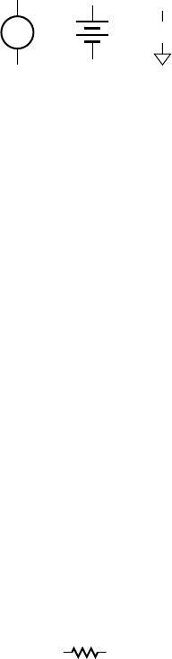
502 APPENDIX B introduction to electronic circuits
models that capture properties of interest to digital designers and that
ignore more detailed effects that are generally not relevant.
B.1.1 VOLTAGE SOURCES
One of the simplest components to describe is a constant voltage source,
which we can represent graphically using the symbol at the left of
Figure B.1. The voltage difference between its positive terminal (marked )
and its negative terminal (marked ) is a constant. Voltage sources are
usually used to provide operating power to digital circuits, either in the
form of batteries (whose symbol is shown in the center of Figure B.1), or
power supply units connected to the mains supply. In this book, we use the
symbols shown at the right of Figure B.1: the top symbol for a positive-
voltage power supply and the bottom symbol for a 0V ground. Since volt-
ages are all relative, labeling the ground as 0V is nominal. Other voltages
are then measured relative to that reference.
An ideal voltage source maintains the constant voltage difference
between its terminals regardless of the current flowing through them.
Real voltage sources used as power supplies can only do that for a limited
range of current flow. Within that range, the voltage is approximately
constant within specified bounds. However, once the current exceeds a
specified limit, the power supply may either reduce the voltage or fail. We
would normally design a system so that the current drawn from a power
supply remains within the specified limits, with some margin, to avoid the
possibility of failure.
B.1.2 RESISTORS
A resistor (Figure B.2) is a component whose voltage drop across its
terminals is linearly related to the current flowing through the terminals.
This property is expressed in Ohm’s law:
V IR (B.1)
For an ideal resistor, the resistance R is constant. In practice, it is slightly
dependent on temperature and other effects, but we can usually ignore
those dependencies in digital circuit design. For practical resistors, the
resistance, measured in ohms (Ω), can range from around 1Ω to 1MΩ.
Since there is a voltage drop across a resistor and current flowing
through it, there is work done. A resistor converts electrical energy into
heat, with the power being the product of voltage and current:
P VI I
2
R V
2
/R (B.2)
+
–
+
–
+V
FIGURE B.1 Symbols for
a voltage source (left), a battery
(center), power supply (top right),
and ground (bottom right).
FIGURE B.2 Symbol for a
resistor.

The generated heat must be dissipated by the resistor, or it will overheat
and fail. Different kinds of physical resistors used in electronic circuits
range in power dissipation capacity from 100mW to 10W.
An important point to note about the relationship between voltage
and current for a resistor is that it is not time dependent. The voltage at
any given instant depends only on the current at that instant, and vice
versa. This stems from the fact that resistors do not store energy, they
simply transform it.
B.1.3 CAPACITORS
A capacitor (Figure B.3) is a component that does store energy, rather
than dissipating it as heat. As the symbol suggests, a capacitor conceptu-
ally consists of two plates, separated by an insulator. Current, consisting
of a flow of charge, transports charge away from one plate and onto the
other, creating an electric field between the plates. This results in a voltage
difference across the plates, and hence between the two terminals of the
capacitor. The relationship between the voltage and the stored charge is
Q CV (B.3)
where the constant C is the capacitance, measured in Farads. Since we
are usually interested in current, not charge storage, we can take the time
derivative of this equation, recognizing that I, Q and V are functions of
time:
I
dQ
dt
C
dV
dt
(B.4)
This equation shows that the behavior of a capacitor is dynamic, that
is, time dependent. For example, we cannot determine the current flowing
through the terminals of a capacitor simply by measuring the instanta-
neous voltage across the terminals; we need to know how fast the volt-
age is changing. The time-dependent behavior is the main cause of delay
in digital circuits. However, the fact that a capacitor stores energy also
allows it to be used as a storage element, giving us time-dependent behav-
ior where needed in digital systems.
Practical capacitors come in a range of capacitance, from a few
picoFarads (1pF 10
12
F) to thousands of microFarads (1µF 10
6
F).
Capacitances in digital circuits are usually toward the smaller end of the
range, either in capacitors that are deliberately included in circuits, or in
stray capacitances that arise between adjacent conductors in the circuit.
B.1.4 INDUCTORS
An inductor (Figure B.4) is another component that stores energy, but in
the form of a magnetic field. As the symbol suggests, one form of inductor
B.1 Components APPENDIX B 503
FIGURE B.3 Symbol for a
capacitor.
FIGURE B.4 Symbol for an
inductor.
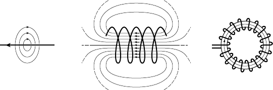
504 APPENDIX B introduction to electronic circuits
FIGURE B.5 Magnetic
fi elds around current-carrying
conductors.
is a helical coil of wire. Even a straight wire conducting current creates a
magnetic field, as shown at the left of Figure B.5. Coiling the wire concen-
trates the field, as shown in the center of the figure, and winding the coil
around a toroidal core with magnetic permeability ideally confines the
field to the core, as shown at the right of the figure. (In a real core, there
will be some stray leakage field.)
If the current through the inductor is constant, the magnetic field does
not change, and the voltage across the inductor is zero. When the current
changes, the magnetic field changes. This changing magnetic field induces
a voltage difference across the inductor, which tends to oppose the current
change. The relationship between the voltage and current change is
V L
dI
dt
(B.5)
where V and I are functions of time, and L is a constant called the induc-
tance, measured in Henries. Thus, the behavior of an inductor, like that
of a capacitor, is dynamic. Practical inductors used in electronic circuits
have inductance in the range of a few microHenries (1µH 10
6
H) to
a few milliHenries (1mH 10
3
H). However, most of the inductors we
encounter in digital circuits are parasitic, rather than being components
deliberately included in a design. We discuss the effects of parasitic induc-
tance on digital circuits in Chapter 6.
B.1.5 MOSFETS
Nearly all digital circuits these days are made from metal-oxide semicon-
ductor field-effect transistors (MOSFETs) fabricated on the surface of a
crystalline silicon wafer. The manufacturing process adds atoms of impu-
rities in selected areas of the silicon, and builds thin layers of material on
the surface. The resulting structure for an n-channel MOSFET, along with
its circuit symbol, is shown in Figure B.6. The pure silicon material forms
a regular crystal lattice, with four bonds between neighboring atoms,
since silicon is a Group IV element. The n regions are areas that have been
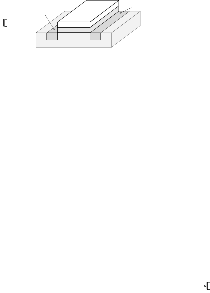
doped (infused) with atoms of an element from Group V of the periodic
table. These atoms have one more valence electron than the silicon atoms,
so n-type material has a surplus of electrons. The p substrate is an area
that has been doped with atoms of an element from Group III of the
periodic table, which have one less valence electron than silicon. Hence,
p-type material has “holes” corresponding to missing lattice bonds. The
gate oxide is a thin insulating layer made of silicon dioxide, and the gate is
a conducting layer made of polycrystalline silicon (polysilicon). Conduct-
ing contacts with the n-type source and drain terminals are usually made
with metal, typically copper in modern circuits.
When the gate terminal is at the same voltage as the substrate, no
current can flow between the source and drain terminals. However, when
a positive voltage is applied to the gate, electrons are attracted toward it.
If the gate voltage is greater than a threshold voltage, sufficient electrons
are attracted to form an n-type channel immediately under the gate oxide.
This channel can conduct current between the source and drain terminals.
Note that no current flows between the gate and the source, drain, or
substrate, due to the insulation of the gate oxide.
We can also manufacture p-channel MOSFETs on silicon wafers. The
symbol is shown in Figure B.7. The structure is similar to that for n-channel
MOSFETs, but the substrate is made of n-type material and the source
and drain regions are p-type. In a p-channel MOSFET, the threshold volt-
age is negative with respect to the substrate. Applying a negative voltage
to the gate repels electrons. We can think of this conversely as attracting
holes to the area under gate oxide. When there are enough holes, a p-type
channel is formed, allowing current to flow.
In complementary MOS (CMOS) digital circuits, we use both n-channel
and p-channel MOSFETs. We arrange for the substrates of the n-channel
MOSFETs to be connected to the ground voltage (V
SS
0 V) and the sub-
strates of the p-channel MOSFETs to be connected to the positive power-
supply voltage (V
DD
). The threshold voltages for both are then between V
SS
and V
DD
. A gate voltage near V
SS
causes an n-channel transistor to turn off
(not to conduct current between source and drain) and a p-channel transis-
tor to turn on (to conduct current between source and drain). Conversely,
a gate voltage near V
DD
causes an n-channel transistor to turn on and a
p-channel transistor to turn off.
B.1 Components APPENDIX B 505
drain
drain
source
source
gate
gate oxide
gate
nn
p substrate
FIGURE B.6 Symbol for a
MOSFET (left), and structure of an
n-channel MOSFET (right).
FIGURE B.7 Symbol for a
p-channel MOSFET.
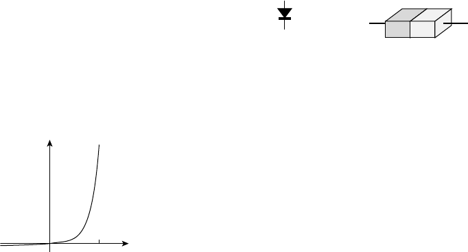
506 APPENDIX B introduction to electronic circuits
Our ideal transistors act as perfect insulators between source and
drain when turned off and as perfect conductors when turned on. In prac-
tice, there is some conduction when the transistor is turned off, though
the resistance is very high. More significantly, there is a nonzero resistance
when the transistor is turned on. This resistance combines with that of
other components and with parasitic capacitance and inductance to cause
nonideal effects that we discuss in Chapters 1 and 6.
Another important property of MOSFETs is the gate capacitance.
The gate and the substrate are two conductive plates separated by a thin
layer of insulator. This is the structure described for a capacitor. The gate
capacitance has some adverse effects, described in Chapter 1, but is is also
central to construction of certain kinds of memory components described
in Chapter 5.
B.1.6 DIODES
In Section B.1.5, we described the use of n-type and p-type regions in
silicon to form MOSFETs. If we manufacture a silicon device with an n
region immediately adjacent to a p region, we form a diode, illustrated in
Figure B.8. For an ideal diode, if the voltage at the anode is positive with
respect to the cathode, the diode is forward biased and acts like a conductor.
On the other hand, if the voltage at the anode is negative with respect to
the cathode, the diode is reverse biased and acts like an insulator.
In practice, the behavior of a diode is more complex than this two-
state ideal model suggests. The actual current/voltage relationship is closer
to that shown in Figure B.9. As the forward voltage increases, the current
increases exponentially. For the ranges of voltages seen in digital circuits,
we can approximate this behavior with a threshold voltage of around
0.7 V. Below the threshold, the current flow is small, approximating an
insulator. Above the threshold, the current flow is large, approximating
a conductor.
The two-state behavior of a diode arises from the electrical effects
that occur in the narrow junction region between the p-type and n-type
materials. In a silicon diode doped with the usual Group III and Group V
elements used in digital IC manufacture (elements such as boron or alu-
minium in Group III and phosphorus in Group V), the power consumed in
the diode is dissipated as heat. However, if the silicon is doped with other
anode
anode
cathode
cathode
np
FIGURE B.8 Symbol for a
diode (left), and its silicon structure
(right).
0.7V
V
I
FIGURE B.9 Current/voltage
characteristics of a diode.
B.1 Components APPENDIX B 507
combinations of elements, some of the energy is emitted in the form of
photons. Such diodes are called light-emitting diodes (LEDs). The wave-
lengths of light emitted range from infrared through the visible spectrum
to blue, depending on the materials used and the construction of the diode.
For some LEDs, the substrate material is not silicon, but combinations of
Group III and V elements manufactured to form crystalline lattices. In
LEDs, the threshold voltage is typically larger than 0.7 V, ranging up to
three or four volts for some high-energy short-wavelength LEDS.
B.1.7
BIPOLAR TRANSISTORS
In Section B.1.6, we saw that we can form a diode at the junction between
n-type and p-type materials in silicon. If we sandwich three layers, we
form a bipolar transistor. Figure B.10 shows an NPN transistor, in which
a layer of p-type material is sandwiched between layers of n-type material.
The three terminals are called the base, emitter and collector. In an ideal
NPN transistor, the current flowing between the emitter and collector
terminals is proportional to the current flowing into the base, typically by
a factor of 100 or so. This property allows a transistor to be used as an
amplifier. However, for digital applications, we usually use transistors in
an operating region called saturation. In that case, absence of base cur-
rent turns the transistor off (no emitter-collector current), and sufficient
base current turns the transistor on (the emitter-collector path conducts
current). This is similar in operation to a MOSFET, but it is current that
controls the device, not voltage.
We can also make a PNP transistor by sandwiching a layer of n-type
material between layers of p-type material. The symbol for a PNP transis-
tor is shown in Figure B.11. In a PNP transistor, the emitter-collector cur-
rent is controlled by the current flowing out of the base terminal. Thus, it
is complementary to an NPN transistor.
The main advantage of bipolar transistors over MOSFETs in digital
applications is that, when individually packaged, they are somewhat more
robust, being less susceptible to damage from electrostatic discharge.
collector
collector
emitter
emitter
base
base
n
n
p
FIGURE B.10 Symbol for an
NPN bipolar transistor (left), and
its silicon structure (right).
collector
emitter
base
FIGURE B.11 Symbol for a
PNP bipolar transistor.
508 APPENDIX B introduction to electronic circuits
Hence, they are often used in connecting external input/output components
to digital systems.
B.2 CIRCUITS
Now that we have identified the components that we use in digital sys-
tems, we describe the effects of connecting them together with wires. An
ideal wire is a perfect conductor. We can consider it to be a two-terminal
component with equal voltages at the terminals. However, it is generally
simpler just to think of the wires in a circuit as joining terminals of other
components, making their voltages equal and linking their current flows.
We define a circuit to be an interconnection of the terminals of a num-
ber of components. Figure B.12 shows an example of a circuit comprising
several two- and three-terminal components. We call each point at which
nodes
branches
loop
FIGURE B.12 A circuit
consisting of interconnected
components, with nodes, branches
and loops.
two or more terminals are connected a node. Note that the terminals don’t
have to be connected at the same physical point. We think of a wire join-
ing several terminals as a single node. We call each connection through a
component from one node to another a branch. For a two-terminal com-
ponent, the component itself forms a single branch. For a three-terminal
component, there are three branches, one between each pair of terminals.
Finally, we call a closed path through branches of a circuit a loop.
B.2.1 KIRCHHOFF’S LAWS
We can analyze a circuit to determine the current flowing through each
branch (the branch current) and the voltage difference across each branch
(the branch voltage). If all the branch currents and voltages are constant,
the behavior of the circuit is static. Usually, however, the branch currents
and voltages are time dependent, in which case the behavior is dynamic. In
this section, we will identify two laws of circuit behavior that allow us to
build systems of equations relating branch currents and voltages. We can
then solve the equations to determine the circuit behavior. If the behavior
is static, the equations will be algebraic. If the behavior is dynamic, we
may have to solve differential equations.
The first law, Kirchhoff’s current law (KCL), states that the current
flowing out of any node and the current flowing into the node must be the
same; that is, the sum of the currents must be zero. The intuition behind
this law is that charge does not accumulate at nodes of a circuit.
The second law, Kirchhoff’s voltage law (KVL), states that the sum
of the branch voltages around any closed path in a circuit must be zero.
The intuition here is that, if we start at any given node in the path, we
determine the voltage at some other node by accumulating the branch
voltages between the starting node and the other node. When we get back
to the starting node, we should have accumulated the same voltage that
we started with, since a node is an equipotential region.
B.2.2 SERIES AND PARALLEL R, C, AND L
Suppose we connect a voltage source and two resistors, R
1
and R
2
, in the
simple circuit shown in Figure B.13. We say the resistors are connected
in series. Since the current flowing into and out of each node is zero, the
same current I flows through both resistors. Since the accumulated volt-
age around the circuit loop is zero, the sum of the voltages across the
resistors must be V. Recalling Ohm’s law from our discussion of resistor
behavior in Section B.1.2, we can write the following equation describing
the circuit:
V V
1
V
2
IR
1
IR
2
I(R
1
R
2
) (B.6)
This indicates that series combination of resistors behaves in the same
way as a single resistor with resistance equal to the sum of the two indi-
vidual resistances. The analysis can be extended to multiple resistors in
series: the combination is equivalent to a single resistor whose resistance
is the sum of the individual resistances:
R R
1
R
2
R
3
…
(B.7)
Since the sum of the voltages across the two resistors is V, the voltage
at the node between the resistors is a fraction of V given by
V
2
V
R
2
R
1
R
2
(B.8)
For this reason, we sometimes call a series connection of resistors a voltage
divider.
B.2 Circuits APPENDIX B 509
+
–
V
1
R
1
R
2
V
I
V
2
FIGURE B.13 A circuit with
two resistors in series.
510 APPENDIX B introduction to electronic circuits
We can perform a similar analysis for a circuit comprising two
resistors connected in parallel, as shown in Figure B.14. In this case, the
voltage across each resistor is V, since each resistor is part of a loop con-
taining the resistor and the voltage source. Since the net current into each
node is zero, the current I is split between I
1
and I
2
. Thus, we can write
the equation:
I I
1
I
2
V
R
1
V
R
2
V
(
R
1
R
2
R
1
R
2
)
(B.9)
In other words, the parallel combination of resistors behaves in the same
way as a single resistor with resistance given by:
R
R
1
R
2
R
1
R
2
or
1
R
1
R
1
1
R
2
(B.10)
We can generalize this to a parallel connection of multiple resistors, which
has an equivalent resistance given by
1
R
1
R
1
1
R
2
1
R
3
…
(B.11)
Having performed this analysis for circuits with resistors in series and
in parallel, we can perform similar analyses with capacitors and induc-
tors. In the case of capacitors connected in series, we note that the same
current flows through all capacitors, and so the same charge Q (being the
integral of current) accumulates on each capacitor:
V
Q
C
V
1
V
2
V
3
…
Q
C
1
Q
C
2
Q
C
3
…
(B.12)
Dividing by Q gives the equivalent capacitance for capacitors connected
in series:
1
C
1
C
1
1
C
2
1
C
3
…
(B.13)
For capacitors connected in parallel, the voltage across each capacitor is
V, and the current is split between the branches. Integrating the currents
gives the total charge as the sum of the individual capacitors’ charges:
Q VC Q
1
Q
2
Q
3
…
VC
1
VC
2
VC
3
…
(B.14)
+
–
I
1
R
1
R
2
V
I
I
2
FIGURE B.14 A circuit with
two resistors in parallel.
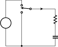
Dividing by V gives the equivalent capacitance for capacitors connected
in parallel:
C C
1
C
2
C
3
…
(B.15)
Similarly, for inductors connected in series, the equivalent inductance is
L L
1
L
2
L
3
…
(B.16)
and for inductors connected in parallel, the equivalent inductance is
1
L
1
L
1
1
L
2
1
L
3
…
(B.17)
B.2.3 RC CIRCUITS
A number of nonideal effects in digital circuits arise from combinations of
resistors and capacitors as circuit components. The components are usu-
ally not designed into the circuits but arise as properties of the transistors,
wires, and packaging of real components. We will start with analysis of a
simple circuit consisting of a resistor and capacitor connected in series, as
shown in Figure B.15, driven by a switched voltage source between a low
voltage (0V) and a high voltage (V). Assume initially, at time t 0, that
there is no charge accumulated on the capacitor, so the voltage V
C
is 0V,
and that the switch is in the 0V state. KVL and KCL tell us that V
R
is also
0V and that the current I is zero.
Now suppose that the switch changes at t 0 to the nonzero voltage V.
Since there is no charge on the capacitor, V
C
is still 0V, so the full volt-
age V appears across the resistor. This causes current to flow, starting to
charge the capacitor. As charge accumulates over time, V
C
increases and
V
R
decreases. To determine the voltage over time at the node between the
resistor and the capacitor, we note that
V V
R
V
C
IR V
C
(B.18)
and that
I C
dV
C
dt
(B.19)
Substituting and rearranging gives the first-order differential equation:
RC
dV
C
dt
V
C
V 0 (B.20)
The solution of this equation gives the following formula for V
C
as a func-
tion of time:
V
C
(t) V
(
1 e
t/RC
)
(B.21)
+
–
V
R
R
C
V
I
V
C
FIGURE B.15 A circuit with
a resistor and a capacitor in series.
B.2 Circuits
APPENDIX B 511
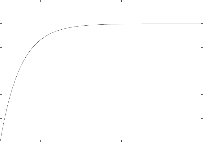
512 APPENDIX B introduction to electronic circuits
Figure B.16 shows a graph of the voltage plotted against time with V 5.0
and RC 0.001. The voltage approaches V asymptotically, reaching
approximately 63% of the value after a time interval given by RC. We
call this interval the time constant of the circuit.
0
1
2
3
4
5
6
0 0.002 0.004 0.006 0.008 0.01
FIGURE B.16 Graph of
capacitor voltage as it charges
through a resistor from a
voltage source.
We simplified the analysis above by assuming an initial voltage of 0V.
In general, if the initial voltage across the capacitor is V
0
, and the driving
voltage changes from V
0
to V, the voltage on the capacitor is given by the
function:
V
C
(t) V (V
0
V) e
t/RC
(B.22)
Thus, if the driving voltage switches periodically between 0V and V, the
voltage on the capacitor is as shown in Figure B.17.
B.2.4 RLC CIRCUITS
While we consider ideal wires to be pure conductors, real wires, especially
long ones, have nonzero inductance. This, combined with parasitic capac-
itance and resistance in various components, leads to a number of the
signal integrity issues that we discussed in Chapter 6. We can understand
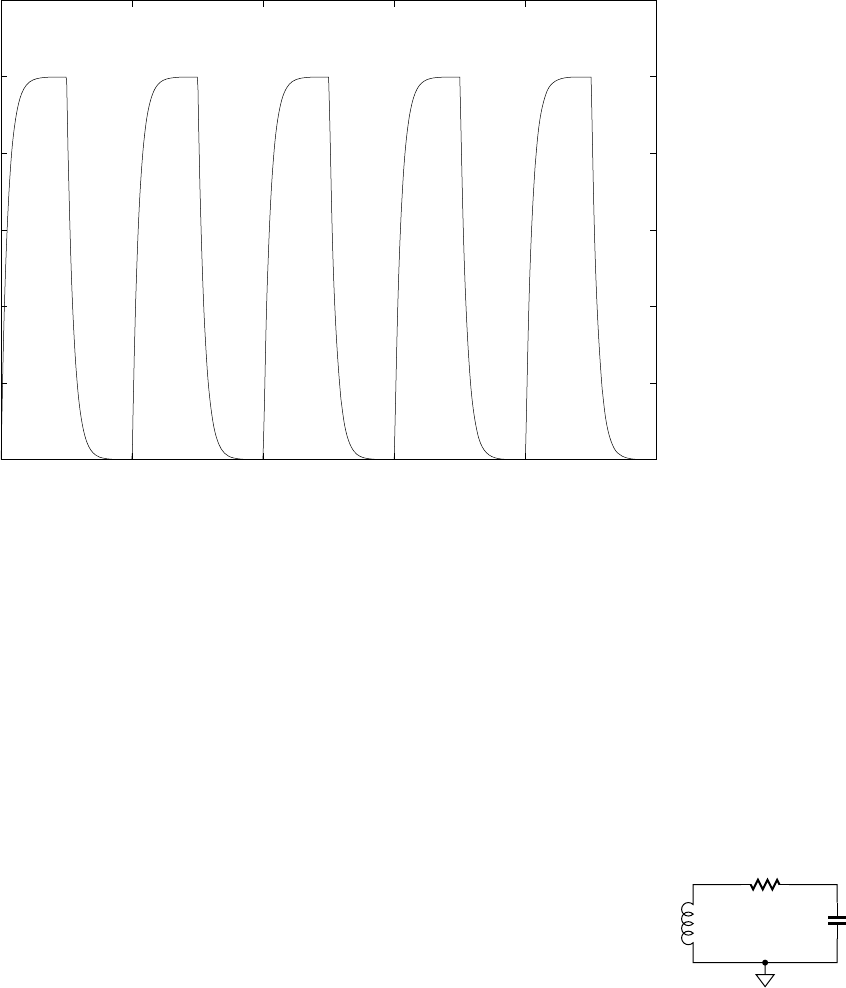
these effects by considering a series connection of a resistor, a capacitor
and an inductor, as shown in Figure B.18. In practice, the resistor might
be the effective on resistance of a transistor, the capacitor might be the
gate capacitance of a transistor connected to a component input, and the
inductor might be the series inductance of the wire connecting them.
We start our analysis of the RLC circuit by considering KCL at the
nodes on either side of the resistor. For the node on the right, the sum of the
currents through the capacitor and resistor is zero, giving the equation:
C
dV
C
dt
V
C
V
L
R
0
(B.23)
We can rearrange this to express V
L
in terms of V
C
:
V
L
RC
dV
C
dt
V
C
(B.24)
For the node on the left, the sum of the currents through the inductor
and resistor is zero. We can determine the current through the inductor by
integrating Equation B.5, giving the equation:
V
C
V
L
R
1
L
t
V
L
dt
~
0 (B.25)
V
C
V
L
R
CL
FIGURE B.18 A series RLC
circuit.
B.2 Circuits
APPENDIX B 513
0
1
2
3
4
5
6
0 0.02 0.04 0.06 0.08 0.1
FIGURE B.17 Graph of
capacitor voltage with the driving
voltage switching periodically.
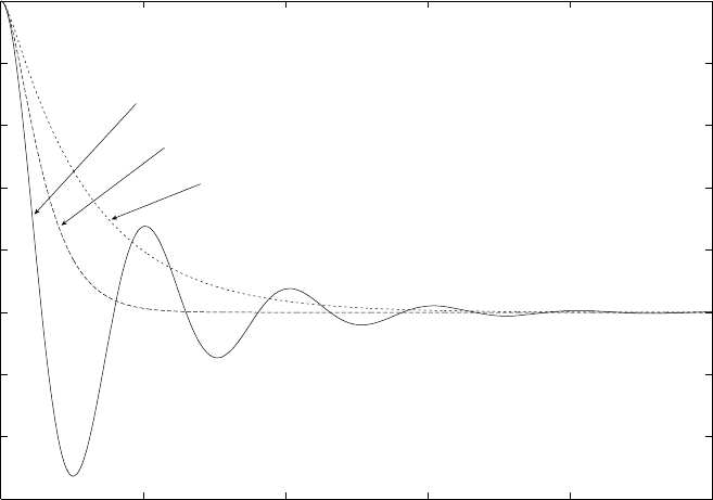
514 APPENDIX B introduction to electronic circuits
Next, we substitute Equation B.24 into Equation B.25, divide by C,
and differentiate with respect to t to yield the following second-order
differential equation for V
C
:
d
2
V
C
dt
2
R
L
dV
C
dt
1
LC
V
C
0 (B.26)
This form of equation describes a resonant harmonic system with
fundamental frequency:
0
1
LC
(B.27)
and damping factor:
1
2
R
L
(B.28)
If
0
, we say the circuit is underdamped. From a nonzero initial state,
the voltage V
C
oscillates sinusoidally, with the amplitude decaying expo-
nentially. If
0
, we say the circuit is critically damped. The voltage V
C
decays toward zero in the minimal time possible. Finally, if
0
, we say
the circuit is overdamped. The voltage V
C
decays toward zero, but settles
at a slower rate than in a critically damped circuit. These three cases are
illustrated in Figure B.19.
-3
-2
-1
0
1
2
3
4
5
0 0.0002 0.0004 0.0006 0.0008 0.001
Underdamped
Critically damped
Overdamped
FIGURE B.19 The behavior
of underdamped, critically damped
and overdamped RLC circuits.
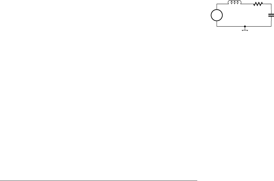
In practical systems, we are interested in the RLC circuit’s response to
changes in a driving voltage. The driven circuit is illustrated in Figure B.20.
The voltage source represents an output from one part of a system driv-
ing the input to another part. The node at which V
C
is measured repre-
sents the input. We can perform a similar analysis for this circuit, giving
the following differential equation for V
C
:
d
2
VC
dt
2
R
L
dV
C
dt
1
LC
V
C
1
LC
V (B.29)
The behavior of this circuit depends on the function V of time. For
analyzing digital circuits, we consider V to be a step function, chang-
ing from zero to some given voltage level, or vice versa. The behavior in
response to a step from a positive voltage to 0V is as shown in Figure B.19,
since in that case V 0. This indicates that the voltage seen on the capaci-
tor may undershoot and “ring” before settling at its final level. Similarly,
the behavior in response to a step from 0V to a positive voltage involves
possible overshoot and ringing before settling. Increasing the resistance
can help to dampen the ringing, at the expense of a slower transition to
the final voltage level. Decreasing parasitic capacitance and inductance
can help by increasing the fundamental frequency, making the circuit
respond faster.
B.3 FURTHER READING
Foundations of Analog and Digital Electronic Circuits, Anant Agarwal
and Jeffrey H. Lang, Morgan Kaufmann Publishers, 2005.
CMOS VLSI Design: A Circuits and Systems Perspective, 3rd Edition,
Neil H. E. Weste and David Harris, Addison-Wesley, 2005.
B.3 Further Reading APPENDIX B 515
V
C
V
L
V
R
C
L
+
–
FIGURE B.20 An RLC circuit
driven by a voltage source.
This page intentionally left blank
517
appendix c
verilog for synthesis
Throughout this book, we have used Verilog, both for description of a
digital circuit under design and for verification testbenches. Our design
methodology involves use of synthesis tools to transform Verilog design
descriptions expressed at the register-transfer level of abstraction into
implementations at the gate level. The style of Verilog that we write for
RTL design descriptions differs from that for testbenches, since not all
aspects of testbenches can sensibly be implemented in hardware. Most
RTL synthesis tools only accept Verilog descriptions that are written
in a subset of the language that can sensibly be implemented in hard-
ware. Testbench code, on the other hand, is more like code in general
purpose programming languages, and can use the full suite of language
features.
In this Appendix, we describe a subset of Verilog that is accepted by
most RTL synthesis tools. We have used this subset in examples through-
out the book. Most tools will accept a greater subset of the language
than that described here. However, if we write code using such language
features accepted by one tool, the code may not be portable for use with
other tools.
C.1 DATA TYPES AND OPERATIONS
In this book, we have consistently used single-bit nets and variables for
single-bit signals and vector nets and variables for multibit signals. These
types are accepted for synthesis. We can perform operations on values of
these types, such as logical operations (&&, || and !), bit-wise operations
(&, |, ~ etc.), shift operations (<<, >> etc.), the conditional operator (... ?
... : ...
), concatenation ({..., ...}), bit select and part select. These operations
can be implemented by synthesis tools.
In this book, we also described the real data type. Synthesis tools typi-
cally do not support use of real numeric values and operations, since the
hardware required to implement them is much more complex than that for
integer types. The hardware is typically sequential, and varies in internal
organization depending on the application requirements. While synthesis
may be feasible for some specialized applications, for other applications,
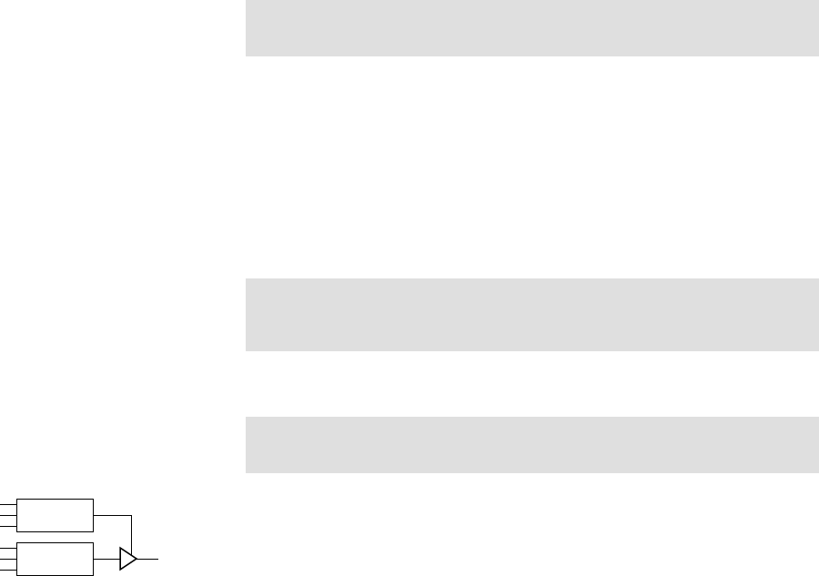
518 APPENDIX C verilog for synthesis
we would expect to implement floating-point operations using library
components or components created by generator tools.
C.2 COMBINATIONAL FUNCTIONS
Combinational circuits, discussed in Chapter 2, use the values of one or
more inputs to determine the value of each output. Verilog allows us to
express such behavior using continuous assignment statements within
a module. Each such assignment statement assigns to a target net that
represents an output of a combinational logic block.
An assignment is of the form:
assign target = expression;
in which the target is a net name, and the expression represents the
function performed by the combinational circuit. The expression includes
the names of input nets and variables, and combines their values using
the operators that we mentioned in Section C.1. The expression must not
include any reference to the target net, since that would imply a feedback
loop, and the circuit would not be combinational. Moreover, we must not
imply feedback indirectly with multiple assignment statements, such as
the following:
assign s1 = a & b & s2;
assign s2 = c | s1;
We can identify a special case of the continuous assignment:
assign target = condition ? expression : 1'bz;
In this case, a synthesis tool would infer a tristate driver, as shown in
Figure C.1, with its input connected to logic inferred from the expression,
and its enable input connected to logic inferred from the condition. In the
case of the target being a vector, the high-impedance value 1'bz is replaced
by a vector of high-impedance values, such as 8'bzzzzzzzz.
In some cases, we might find it more convenient to express combi-
national logic using an always block rather than a collection of continu-
ous assignment statements. Typical cases are combinational logic blocks
with multiple outputs all controlled by the same or similar conditions,
or where the expressions are complex and are more readily understood
expression
condition
target
FIGURE C.1 Hardware
inferred for an assignment with
1'bz as an alternative.
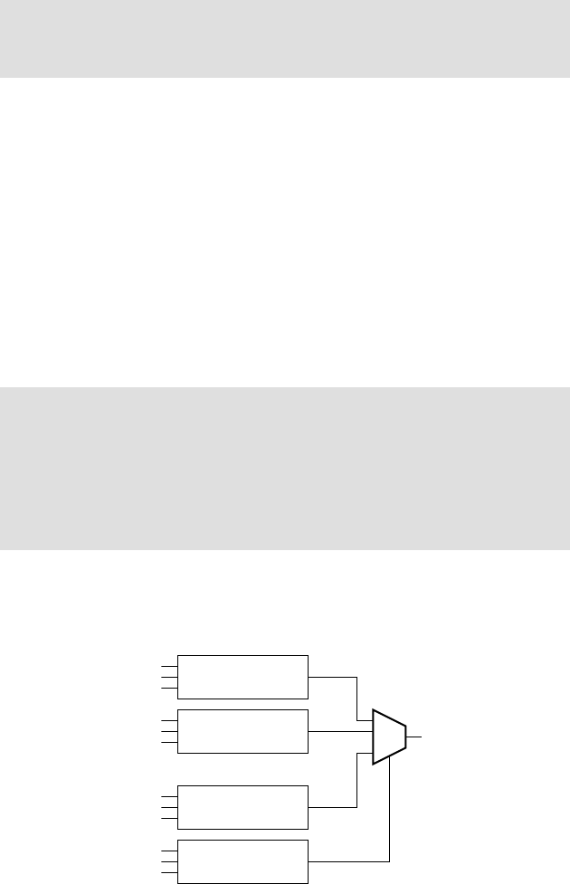
by being broken into smaller subexpressions. For a synthesis tool to be
able to infer combinational logic from an always block, we must follow a
number of rules. First, the format of the block must be
always @(event-list)
statement;
The event list is a list of all of the inputs to the combinational block. This
ensures that whenever any of the inputs changes value, the block deter-
mines new values for the outputs. If any input is read in the block but is
not in the event list, the synthesis tool would typically issue a warning
message. One simple way to ensure that we don’t inadvertently omit any
input from the event list is to use an alternate form, @*, which stands for
“all inputs read in the block.” While this is recommended, it was intro-
duced into Verilog in a relatively recent revision of the language, and may
not be uniformly supported by all synthesis tools.
The statement in the always block can be a conditional statement,
such as a case statement or if statement, containing nested assignments.
An example is an always block of the form:
always @*
case (select-expression)
choice-1: target = expression-1;
choice-2: target = expression-2;
...
choice-n: target = expression-n;
endcase
A synthesis tool could infer a multiplexer, as shown in Figure C.2, pro-
vided the choice values were distinct and included all possible values of
C.2 Combinational Functions APPENDIX C 519
FIGURE C.2 Hardware
inferred for a selected assignment.
1
2
…
n
expression-1
expression-2
expression-n
select-expression
…
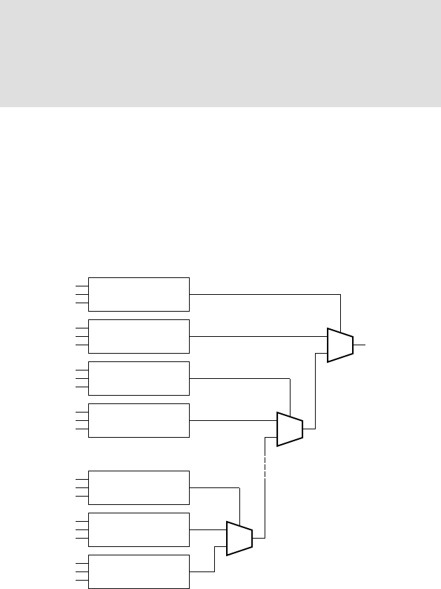
520 APPENDIX C verilog for synthesis
the select expression. The select inputs of the multiplexer are connected to
the output of the combinational logic inferred from the select expression.
Each of the assignment expressions would be synthesized to combinational
logic connected to the particular data input of the multiplexer identified
by the corresponding choice value. The choice values are expressions, but
they must not involve any inputs. Usually, they are just literal values.
The effect of inclusion of an if statement is illustrated by an always
block of the form:
always @*
if (condition-1) target = expression-1;
else if (condition-1) target = expression-1;
...
else target = expression-n;
Each of the expressions and conditions implies combinational logic. The
outputs of the expression logic are connected to decision logic driven by
the condition logic, such as that shown in Figure C.3. Since the condi-
tions are tested one by one until a true condition is found, the decision
logic is priority based, with conditions appearing earlier in the conditional
assignment having priority over those appearing later. As a consequence,
the propagation delay for the inferred logic may be as long as the sum
of propagation delays of the inferred decision component. Of course, a
expression-1
expression-2
condition-1
condition-2
…
0
1
0
1
expression-n–1
expression-n
condition-n–1
0
1
FIGURE C.3 Hardware
inferred for a conditional
assignment.

synthesis tool may optimize the circuit, and may be able to implement
the assignment as a single multiplexer if the conditions are mutually
exclusive.
If a combinational logic block has multiple outputs, we can include
multiple assignments within an always block. In that case, we need to
group the assignment statements in a begin/end block. The block is of the
form:
always @(event-list) begin
statement-1;
statement-2;
...
statement-n;
end
This form has the benefit of allowing us to extract common parts
of complex expressions into assignments to intermediate variables. For
example, instead of writing
assign s1 = (c * a) + (b << 4) + offset1;
assign s2 = (c * a) + (b << 4) + offset2;
we might declare a variable for the common part of the expression and
use it as follows:
reg [17:0] base;
...
always @(a, b, c, offset1, offset2) begin
base = (c * a) + (b << 4);
s1 = base + offset1;
s2 = base + offset2;
end
In this example, the variable base is not an input to the combinational
block. It is an intermediate value, since it is assigned a new value each time
the block is activated, and that value is only read in subsequent expres-
sions. For this reason, the variable does not need to be included in the
event list (although to include it would not be an error). Note that we need
to use a blocking assignment (written using “”) for the intermediate
variable, since we read the assigned value in the subsequent expressions.
C.2 Combinational Functions APPENDIX C 521

522 APPENDIX C verilog for synthesis
Were we to use a nonblocking assignment (written using “< =”), the value
would not be assigned until completion of the statements in the block.
The expressions written after the assignment would read the old value of
the variable.
One point to note about the use of always blocks to represent com-
binational logic is that the outputs assigned within the block must be
variables, not nets. Thus, they must be declared using reg or integer data
types, not wire. We can choose between blocking assignments or non-
blocking assignments for the output variables, provided we use the same
kind of assignment uniformly for a given variable within a block. The
blocking assignment is preferred, since it is consistent with assignment to
intermediate variables.
The statements within an always block representing combinational
logic should all be simple assignments or control-flow statements (if
statements and case statements). All of the expressions and conditions
in control-flow statements should imply combination logic. If we do use
control-flow statements, we must ensure that each variable is assigned in
all possible paths through the block. Otherwise, there is some combina-
tion of input values for which no new output value is determined, implying
storage for the previous value. The block would not exhibit combinational
behavior in that case; instead, it would imply a level-sensitive latch.
The circuit inferred by a synthesis tool has a propagation delay deter-
mined by the gates in the circuit. The delay depends on the particular
technology library used and the circuit’s ultimate placement and routing.
Any delay that we specify in the Verilog code has no effect on the synthe-
sized circuit. Thus, we should generally not write statements in an always
block such as:
#10 s = a + b;
A synthesis tool would ignore the delay in the assignment, or perhaps
issue a warning. We usually only write assignments with delays in test-
bench models for stimulus generation.
C.3 SEQUENTIAL CIRCUITS
As we discussed in Chapter 4, most sequential systems use edge- triggered
clocked timing. For RTL synthesis, we describe the storage elements
involved in such systems (the flip-flops and registers) using always blocks
based on a small number of templates. Whether a block represents a flip-
flop or a register depends on whether the output signal assigned by the
block is a single bit or a vector of bits, respectively.

The simplest form of flip-flop or register updates its output on every
clock cycle. We use the following always-block template to express such
a register:
always @(posedge clock)
target <= input;
A synthesis tool infers a register that updates the target variable with the
value of the input signal on every rising edge of the clock signal. For a
falling-edge-triggered register, we substitute negedge for posedge in the
above block.
More frequently, we use registers with control signals. If the control
signals are synchronous, that is, they take effect only on the active clock
edge, we test for them in order of priority using if statements, but include
only the clock in the event list. An example is the following always block
representing a register with synchronous reset and clock enable:
always (posedge clock)
if (reset) target <= 0;
else if (
clock_en) target <= input;
If, on the other hand, the control signals are asynchronous, we include the
control signals in the event expression. For positive-logic control signals,
we use a posedge event expression and test whether the control signal
is 1. For negative-logic control signals, we use a negedge event expres-
sion and test whether the control signal is 0. An example is the following
always block representing a flip-flop with asynchronous negative-logic
reset and asynchronous positive-logic preset:
always @(posedge clock, negedge reset, posedge preset)
if (~reset) target <= 0
else if (preset) target <= 1;
else target <= input;
We can combine synchronous and asynchronous control in a single
register. We include event expressions for the clock and asynchronous
control inputs in the event list, and test for asynchronous control condi-
tions before testing for synchronous control conditions. This is illustrated
C.3 Sequential Circuits APPENDIX C 523

524 APPENDIX C verilog for synthesis
by the following example, with asynchronous reset and synchronous
clock enable:
always @(posedge clock, posedge reset)
if (reset) target <= 0;
else if (clock_en) target <= input;
RTL designs typically involve combinational logic connected to the
inputs of registers. While we can use separate continuous assignments
and always blocks to model the logic and the registers, respectively, it is
often clearer to combine the two. The registers are modeled by always
blocks according to the templates we described above, and the combi-
national logic is modeled by expressions on the right-hand sides of the
assignments within the always blocks. For example, the following block
represents a combinational multiplier connected to the input of a register
with synchronous control signals.
always @(posedge clock)
if (
reset) target <= 0;
else if (clock_en) target <= a * b;
We can extend this principle to represent multiplexers and other more
involved combinational circuits, using if statements and case statements
within always blocks representing registers. For example, the following
represents a register whose input comes from a multiplexer:
always @(posedge clock)
if (reset) target <= 0;
else if (clock_en)
case (select_expr)
choice_1: target <= expression_1;
choice_2: target <= expression_2;
...
default: target <= ...;
endcase
Two special cases of registers with combinational logic are counters
and shift registers, each of which includes a combinational function of its
output to determine its input. A counter simply increments or decrements
its output, for example:
always @(posedge clock)
if (reset) target <= 0;
else if (count_en) target <= target + 1;

A shift register forms its input from a shifted version of its output, to
which is concatenated an input bit:
always @(posedge clock)
if (
reset) target <= 0;
else if (shift_en) target <= {data_in, target[3:1]};
If an RTL design includes several registers that are all clocked together
and all have the same control signals, we can combine them into a single
always block, for example:
always @(posedge clock)
if (
reset) begin
target1 <= 0;
target2 <= 0;
end
else if (
clock_en) begin
target1 <= expression1;
target2 <= expression2;
end
A synthesis tool would infer the required number of registers, with inputs
for each taken from the corresponding inferred combinational logic. The
combined block is a more succinct model than separate blocks.
C.3.1 FINITE-STATE MACHINES
We introduced finite-state machines (FSMs) in Chapter 4, and described
their use in the control sections of sequential digital systems. We use param-
eter definitions to specify the set of states for the FSM, for example:
parameter [1:0] state1 = 2'00, state2 = 2'01,
state3 = 2'10, state4 = 2'11;
reg [1:0] current_state, next_state;
Each of the parameters represents one of the FSM states. A synthesis
tool would either use the parameter values or select an alternate binary
encoding for the state values to optimize the hardware that it generates.
An FSM is usually implemented using a register to store the current
state and combination logic for the next-state and output functions.
C.3 Sequential Circuits APPENDIX C 525

526 APPENDIX C verilog for synthesis
We can write three separate always blocks for these elements, using the
templates described previously, as follows:
always @(posedge clock) // state register
if (
reset) current_state <= initial-state;
else current_state <= next_state;
always @* // next-state logic
case (current_state)
state1: if (condition-1) next_state = state-value;
else if (condition-2) next_state = state-value;
...
else next_state = state-value;
state2: ...
endcase
always @*// output logic
case (current_state)
state1: begin
moore-output-1 = value; moore-output-2 = value; ...
if (condition-1) begin
mealy-output-1 = value; mealy-output-2 = value; ...
end
else if (condition-2) begin
mealy-output-1 = value; mealy-output-2 = value; ...
...
end
else begin
mealy-output-1 = value; mealy-output-2 = value; ...
end
end
state2: begin
...
end
endcase
Often, the blocks representing the two combinational logic blocks
may be combined, especially if the conditions governing the Mealy-style
outputs are the same as those governing the state transitions. The com-
bined block would be of the form:
always @* // fsm logic
case (current_state)
state1: begin
if (condition-1) begin
next_state = state-value;
mealy-output-1 = value; mealy-output-2 = value; ...
end
(continued)

else if (condition-2) begin
next_state = state-value;
mealy-output-1 = value; mealy-output-2 = value; ...
...
end
else begin
next_state =
state-value;
mealy-output-1 = value; mealy-output-2 = value; ...
end
moore-output-1 = value; moore-output-2 <= value; ...
end
state2: begin
...
end
endcase
In some designs, the FSM outputs are Moore-style and are activated
only during one or two states. In such cases, the output function can
be expressed using simple continuous assignments rather than using an
always block, for example:
assign moore-output-1 = current_state == state1;
assign moore-output-2 = current_state
== state3 || current_state == state4;
C.4 MEMORIES
RTL synthesis support for memories is not as well established as that
for combinational and sequential circuits. Most ASIC designs would use
memories generated using a memory component generator or provided as
library cells by an IP vendor, since memory circuits can be highly customized
in ASICs. On the other hand, synthesis tools can take advantage of the
memory blocks built into most larger FPGAs, and so support inference
of memories from Verilog code targeted at an FPGA implementation. We
should consult the documentation for the tool we plan to use for an FPGA
design to determine how it expects a memory to be described. In this sec-
tion, we outline templates that should be compatible with most FPGA
synthesis tools.
We represent the data stored in a memory using a variable of an array
type. We need to declare the variable, specifying the range of address val-
ues and the type of the data stored in each location, for example:
reg [15:0] data_ram [0:2**18–1];
C.4 Memories
APPENDIX C 527

528 APPENDIX C verilog for synthesis
This describes storage for a memory with 2
18
locations, each of 16 bits.
The memory is then described using an always block that implements
the read and write operations. For example, to describe a flow-through
SSRAM, we can use a block of the form:
always @(posedge clock)
if (enable)
if (write) begin
data_ram[address] <= data-in; data-out <= data-in;
end
else
data-out <= data_ram[address];
Describing read-only memories (ROMs) is substantially simpler, since
only read operations are required. As for a RAM, we use an array variable
for the data values, for example:
reg [11:0] data_rom [0:128];
The read operation for a ROM can be as simple as an assignment,
such as the following:
assign data-out = data_rom[address];
This represents a combinational ROM, in which the output is a function
of the address. Alternatively, if the ROM is to be implemented using a
synchronous block memory in an FPGA, we can use an always block of
the following form to describe the ROM:
always @(posedge clock)
if (enable) data-out <= data_rom[address];
All that remains is to specify the data values for the ROM. We can use
an initial block for this, for example:
initial begin
data_rom[0] = 12'h000; data_rom[1] = 12'h021;
data_rom[2] = 12'h1B3; data_rom[3] = 12'h7C0;
...
end

However, this is cumbersome for large ROMs. Instead, we can use the
system task $readmemh or $readmemb in the initial block to read hexa-
decimal or binary data, respectively, from a file, for example:
initial $readmemb("file-name", datarom);
The file is expected to contain a sequence of values, either in hexadecimal
or binary format, as appropriate, separated by spaces or line breaks. Val-
ues are read from the file into successive elements of the specified variable
until either the end of the file is reached or all elements of the variable are
loaded.
C.4 Memories APPENDIX C 529
This page intentionally left blank

531
appendix d
the gumnut
microcontroller core
This Appendix is a complete reference for the Gumnut microcontroller
core introduced in Chapter 7. We provide details of the instruction set
and the bus interface for connecting memory and I/O controllers. Docu-
mentation for an assembler and its assembly language are included on the
companion website.
D.1 THE GUMNUT INSTRUCTION SET
The Gumnut has an instruction memory of up to 4096 18-bit instructions
(using 12-bit addresses) and a data memory of 256 bytes (using 8-bit
addresses). When the CPU is reset, it clears the PC to 0 and starts execut-
ing instructions. Within the CPU, there are eight general purpose registers,
named r0 through r7, that can hold data to be operated upon by instruc-
tions. Register r0 is special, in that it is hard-wired to have the value
0, and any updates to it are ignored. The CPU also has two single-bit
condition-code registers called Z (zero) and C (carry). They are set to 1
or cleared to 0 depending on the result of certain instructions, and can be
tested to decide among alternative courses of action in the program.
The complete Gumnut instruction set is summarized in Table D.1.
For the arithmetic and logical instructions, op2 is either a second register
(rs2) or an immediate value (immed). Details of each instruction, includ-
ing its instruction word encoding, are provided in this section.
D.1.1 ARITHMETIC AND LOGICAL INSTRUCTIONS
add rd, rs, rs2
Add values in registers rs and rs2, and place result in register rd. Set C to
carry out of the addition. Set Z to 1 if the result is 0, or to 0 otherwise.
왘
11 01 rd rs rs2
17 16 15 14 13 12 11 10 0123456789
00011 01 rd rs rs2
17 16 15 14 13 12 11 10 0123456789
000

532 APPENDIX D the gumnut microcontroller core
instruction description
Arithmetic and logical instructions
add rd, rs, op2 Add rs and op2, result in rd
addc rd, rs, op2 Add rs and op2 with carry, result in rd
sub rd, rs, op2 Subtract op2 from rs, result in rd
subc rd, rs, op2 Subtract op2 from rs with carry, result in rd
and rd, rs, op2 Logical AND of rs and op2, result in rd
or rd, rs, op2 Logical OR of rs and op2, result i
n rd
xor rd, rs, op2 Logical XOR of rs and op2, result in rd
mask rd, rs, op2 Logical AND of rs and NOT op2, result in rd
Shift instructions
shl rd
,
rs, count Shift rs value left count places, result in rd
shr rd, rs, count Shift rs value right count places, result in rd
rol rd, rs, count Rotate rs value left count places, result in rd
ror rd, rs, count Rotate rs value right count places, result in rd
Memory and I/O instructions
ldm rd, (rs)± offset Load to rd from memory
stm rd, (rs)± offset Store to memory from rd
inp rd, (rs)± offset Input to rd from input controller register
out rd, (rs)± offset Output to output controller register from rd
Branch instructions
bz ±disp Branch if Z is set
bnz ±disp Branch if Z is not set
bc ±disp Branch if C is set
bnc ±disp Branch if C is not set
Jump instructions
jmp addr Jump to addr
jsb addr
Jump to subroutine at
addr
TABLE D.1 The Gumnut
instruction set.
(continued )
add rd, rs, immed
Add value in register rs and the immediate operand immed, and place
result in register rd. Set C to carry out of the addition. Set Z to 1 if the
result is 0, or to 0 otherwise.
addc rd, rs, rs2
Add values in registers rs and rs2 and C, and place result in register rd.
Set C to carry out of the addition. Set Z to 1 if the result is 0, or to 0
otherwise.
addc rd, rs, immed
Add value in register rs, the immediate operand immed, and C, and place
result in register rd. Set C to carry out of the addition. Set Z to 1 if the
result is 0, or to 0 otherwise.
sub rd, rs, rs2
11 01 rd rs rs2
17 16 15 14 13 12 11 10 0123456789
001
Subtract value in register rs2 from value in register rs, and place result in
register rd. Set C to borrow out of the subtraction. Set Z to 1 if the result
is 0, or to 0 otherwise.
왘
왘
왘
왘
00 00 rd rs immed
17 16 15 14 13 12 11 10 0123456789
00 00 rd rs immed
17 16 15 14 13 12 11 10 0123456789
11 01 rd rs rs2
17 16 15 14 13 12 11 10 0123456789
01011 01 rd rs rs2
17 16 15 14 13 12 11 10 0123456789
010
00 10 rd rs immed
17 16 15 14 13 12 11 10 0123456789
00 10 rd rs immed
17 16 15 14 13 12 11 10 0123456789
D.1 The Gumnut Instruction Set APPENDIX D 533
instruction description
Miscellaneous instructions
ret Return from subroutine
reti Return from interrupt
enai Enable interrupts
disi Disable interrupts
wait Wait for interrupts
stby Enter low-power standby mode
TABLE D.1 (continued)
The Gumnut instruction set.

534 APPENDIX D the gumnut microcontroller core
sub rd, rs, immed
Subtract immediate operand immed from value in register rs, and place
result in register rd. Set C to borrow out of the subtraction. Set Z to 1 if
the result is 0, or to 0 otherwise.
subc rd, rs, rs2
Subtract value in register rs2 and C from value in register rs, and place
result in register rd. Set C to borrow out of the subtraction. Set Z to 1 if
the result is 0, or to 0 otherwise.
subc rd, rs, immed
Subtract immediate operand immed and C from value in register rs, and
place result in register rd. Set C to borrow out of the subtraction. Set Z to 1
if the result is 0, or to 0 otherwise.
and rd, rs, rs2
Form logical AND of values in registers rs and rs2, and place result in
register rd. Set C to 0. Set Z to 1 if the result is 0, or to 0 otherwise.
and rd, rs, immed
Form logical AND of value in register rs and the immediate operand
immed, and place result in register rd. Set C to 0. Set Z to 1 if the result
is 0, or to 0 otherwise.
or rd, rs, rs2
Form logical inclusive-OR of values in registers rs and rs2, and place result
in register rd. Set C to 0. Set Z to 1 if the result is 0, or to 0 otherwise.
or rd, rs, immed
Form logical inclusive-OR of value in register rs and the immediate oper-
and immed, and place result in register rd. Set C to 0. Set Z to 1 if the
result is 0, or to 0 otherwise.
왘
왘
왘
왘
왘
왘
왘
00 01 rd rs immed
17 16 15 14 13 12 11 10 0123456789
00 01 rd rs immed
17 16 15 14 13 12 11 10 0123456789
11 01 rd rs rs2
17 16 15 14 13 12 11 10 0123456789
01111 01 rd rs rs2
17 16 15 14 13 12 11 10 0123456789
011
00 11 rd rs immed
17 16 15 14 13 12 11 10 0123456789
00 11 rd rs immed
17 16 15 14 13 12 11 10 0123456789
11 01 rd rs rs2
17 16 15 14 13 12 11 10 0123456789
10011 01 rd rs rs2
17 16 15 14 13 12 11 10 0123456789
100
01 00 rd rs immed
17 16 15 14 13 12 11 10 0123456789
01 00 rd rs immed
17 16 15 14 13 12 11 10 0123456789
11 01 rd rs rs2
17 16 15 14 13 12 11 10 0123456789
11011 01 rd rs rs2
17 16 15 14 13 12 11 10 0123456789
110
01 10 rd rs immed
17 16 15 14 13 12 11 10 0123456789
01 10 rd rs immed
17 16 15 14 13 12 11 10 0123456789
xor rd, rs, rs2
Form logical exclusive-OR of values in registers rs and rs2, and place result
in register rd. Set C to 0. Set Z to 1 if the result is 0, or to 0 otherwise.
xor rd, rs, immed
Form logical exclusive-OR of value in register rs and the immediate
operand immed, and place result in register rd. Set C to 0. Set Z to 1 if the
result is 0, or to 0 otherwise.
mask rd, rs, rs2
Form logical AND of value in register rs and logical NOT of value in rs2,
and place result in register rd. Set C to 0. Set Z to 1 if the result is 0, or
to 0 otherwise.
mask rd, rs, immed
Form logical AND of value in register rs and logical NOT of the immediate
operand immed, and place result in register rd. Set C to 0. Set Z to 1 if the
result is 0, or to 0 otherwise.
D.1.2 SHIFT INSTRUCTIONS
shl rd, rs, count
Perform a logical shift left of the value in register rs by count places, and
place result in register rd. Set C to the value of the last bit shifted past the
left-hand end of the byte. Set Z to 1 if the result is 0, or to 0 otherwise.
shr rd, rs, count
Perform a logical shift right of the value in register rs by count places, and
place result in register rd. Set C to the value of the last bit shifted past the
right-hand end of the byte. Set Z to 1 if the result is 0, or to 0 otherwise.
왘
왘
왘
왘
왘
왘
11 01 rd rs rs2
17 16 15 14 13 12 11 10 0123456789
10111 01 rd rs rs2
17 16 15 14 13 12 11 10 0123456789
101
01 01 rd rs immed
17 16 15 14 13 12 11 10 0123456789
01 01 rd rs immed
17 16 15 14 13 12 11 10 0123456789
11 01 rd rs rs2
17 16 15 14 13 12 11 10 0123456789
11111 01 rd rs rs2
17 16 15 14 13 12 11 10 0123456789
111
01 11 rd rs immed
17 16 15 14 13 12 11 10 0123456789
01 11 rd rs immed
17 16 15 14 13 12 11 10 0123456789
11 000 rd rs count
17 16 15 14 13 12 11 10 0123456789
11 000 rd rs count
17 16 15 14 13 12 11 10 0123456789
11 100 rd rs count
17 16 15 14 13 12 11 10 0123456789
11 100 rd rs count
17 16 15 14 13 12 11 10 0123456789
D.1 The Gumnut Instruction Set APPENDIX D 535
536 APPENDIX D the gumnut microcontroller core
rol rd, rs, count
Rotate the value in register rs left by count places, and place result in
register rd. Set C to the value of the last bit rotated past the left-hand end
of the byte. Set Z to 1 if the result is 0, or to 0 otherwise.
ror rd, rs, count
Rotate the value in register rs right by count places, and place result in
register rd. Set C to the value of the last bit rotated past the right-hand end
of the byte. Set Z to 1 if the result is 0, or to 0 otherwise.
D.1.3 MEMORY AND I/O INSTRUCTIONS
ldm rd, (rs) offset
Load into register rd from the memory location whose address is the sum
of the value in register rs and the value offset. C and Z are unaffected.
stm rd, (rs) offset
Store the value in register rd to the memory location whose address
is the sum of the value in register rs and the value offset. C and Z are
unaffected.
inp rd, (rs) offset
Input into register rd from the I/O controller register whose address
is the sum of the value in register rs and the value offset. C and Z are
unaffected.
out rd, (rs) offset
10 11 rd rs offset
17 16 15 14 13 12 11 10 0123456789
Output the value in register rd to the I/O controller register whose address
is the sum of the value in register rs and the value offset. C and Z are
unaffected.
왘
왘
왘
왘
왘
왘
11 010 rd rs count
17 16 15 14 13 12 11 10 0123456789
11 010 rd rs count
17 16 15 14 13 12 11 10 0123456789
11 110 rd rs count
17 16 15 14 13 12 11 10 0123456789
11 110 rd rs count
17 16 15 14 13 12 11 10 0123456789
10 00 rd rs offset
17 16 15 14 13 12 11 10 0123456789
10 00 rd rs offset
17 16 15 14 13 12 11 10 0123456789
10 10 rd rs offset
17 16 15 14 13 12 11 10 0123456789
10 10 rd rs offset
17 16 15 14 13 12 11 10 0123456789
10 01 rd rs offset
17 16 15 14 13 12 11 10 0123456789
10 01 rd rs offset
17 16 15 14 13 12 11 10 0123456789
D.1.4 BRANCH INSTRUCTIONS
bz ±disp
If Z is 1, branch by adding the value disp to the PC; otherwise, the PC is
unaffected. C and Z are unaffected.
bnz ±disp
If Z is 0, branch by adding the value disp to the PC; otherwise, the PC is
unaffected. C and Z are unaffected.
bc ±disp
If C is 1, branch by adding the value disp to the PC; otherwise, the PC is
unaffected. C and Z are unaffected.
bnc ±disp
If C is 0, branch by adding the value disp to the PC; otherwise, the PC is
unaffected. C and Z are unaffected.
D.1.5 JUMP INSTRUCTIONS
jmp addr
Jump by setting the PC to the value addr. C and Z are unaffected.
jsb addr
Jump to a subroutine by first pushing the value of the PC onto the return-
address stack, and then setting the PC to the value addr. The return-
address stack is eight entries deep. If the stack is full before execution of
the instruction, the bottom entry is lost. C and Z are unaffected.
왘
왘
왘
왘
왘
왘
11 110001 disp
17 16 15 14 13 12 11 10 0123456789
11 110001 disp
17 16 15 14 13 12 11 10 0123456789
11 110011 disp
17 16 15 14 13 12 11 10 0123456789
11 110011 disp
17 16 15 14 13 12 11 10 0123456789
11 11 1001 disp
17 16 15 14 13 12 11 10 0123456789
11 11 1001 disp
17 16 15 14 13 12 11 10 0123456789
11 11 1011 disp
17 16 15 14 13 12 11 10 0123456789
11 11 1011 disp
17 16 15 14 13 12 11 10 0123456789
11 1001 addr
17 16 15 14 13 12 11 10 0123456789
11 1001 addr
17 16 15 14 13 12 11 10 0123456789
111101 addr
17 16 15 14 13 12 11 10 0123456789
111101 addr
17 16 15 14 13 12 11 10 0123456789
D.1 The Gumnut Instruction Set APPENDIX D 537
538 APPENDIX D the gumnut microcontroller core
D.1.6 MISCELLANEOUS INSTRUCTIONS
ret
Return from a subroutine by setting the PC to the value in the top entry
of the return-address stack and then popping the stack. If the stack is
empty before execution of the instruction, the value copied to the PC is
undefined.
reti
Return from an interrupt handler by setting the PC, C and Z to the values
saved when the interrupt was acknowledged and by re-enabling inter-
rupts. If this instruction is executed other than in an interrupt handler, the
values written to PC, C and Z are undefined.
enai
Enable response to interrupts.
disi
Disable response to interrupts.
wait
Suspend execution and wait until an interrupt occurs.
stby
Enter low-power standby mode until an interrupt occurs.
D.2 THE GUMNUT BUS INTERFACE
The Gumnut microcontroller core uses Wishbone buses to connect to the
instruction memory, the data memory, and the I/O controller ports, as
shown in Figure D.1. Each of the buses uses classic single-read and single-
write bus cycles, as described in the Wishbone bus specification included
왘
왘
왘
왘
왘
왘
11 1 0000111
17 16 15 14 13 12 11 10 0123456789
11 1 0000111
17 16 15 14 13 12 11 10 0123456789
11 1 000111 1
17 16 15 14 13 12 11 10 0123456789
11 1 000111 1
17 16 15 14 13 12 11 10 0123456789
11 1 0010111
17 16 15 14 13 12 11 10 0123456789
11 1 0010111
17 16 15 14 13 12 11 10 0123456789
11 1 0011111
17 16 15 14 13 12 11 10 0123456789
11 1 0011111
17 16 15 14 13 12 11 10 0123456789
11 1 0100111
17 16 15 14 13 12 11 10 0123456789
11 1 0100111
17 16 15 14 13 12 11 10 0123456789
11 1 0101111
17 16 15 14 13 12 11 10 0123456789
11 1 0101111
17 16 15 14 13 12 11 10 0123456789
for reference on the companion website. The companion website also
contains Verilog behavioral and synthesizable RTL models for the Gumnut,
as well as models for an instruction memory and a data memory. These models
can be used for embedded system designs implemented in FPGAs or ASICs.
The website also contains a simple assembler, called gasm, together with
documentation and sample assembly-language programs.
inst_adr_o
inst_dat_i
rst_i
gumnut
inst_cyc_o
inst_stb_o
inst_ack_i
data_adr_o
data_dat_i
data_dat_o
data_cyc_o
data_stb_o
data_ack_i
data_we_o
port_adr_o
port_dat_i
port_dat_o
port_cyc_o
port_stb_o
port_ack_i
port_we_o
int_ack
int_req
clk_i
FIGURE D.1 Wishbone bus
connections on the Gumnut core.
D.2 The Gumnut Bus Interface
APPENDIX D 539
This page intentionally left blank
index
541
2s complement, 119
7-segment decoders, 66–68, 235–
237, 254–255, 322–326
A
absorption laws, 49
abstraction, 2
accelerators
address generation, 395–397
Amdahl’s Law, 381
architecture, 382
blocks, 384
concepts, 282–283, 379–385
control and status registers, 398
control sequencing, 397–406
convolution/convolution mask,
386
data dependency graph, 388
datapath, 390–395
dependencies, 380
DMA, 383–384
FSM and control, 400–406
instruction-level parallelism,
380
kernel of algorithm, 381
parallelism, 379, 388
pipelining, 382, 395
simulations, 415–417
slave bus model, 398–400
Sobel edge detection pseudo-
code, 387–390
speedup calculation example,
381–382
state transition diagram for
control section, 401
streams, 384
synthesize and implement
Sobel design, 445–448
verifying, 407–417
video edge-detection case
study, 386–407
accelerometers, 319
access time, memory, 221–222
accumulator, 159
acknowledge interrupt request,
364
Actel Corporat
ion, 71, 266, 268,
284
active-high logic, 4, 71
active-low logic, 4, 71–73
naming convention (_N), 73,
160
negation “bubbles” on
components, 72
night-light circuit, 71–72
actuators and valves, 316,
326–327
ad hoc system models, 427
adders
carry-lookahead, 100
carry-lookahead generator,
100
combinational multiplier for
partial products, 113–114
defined, 96
fast-carry-chain, 99
full adder circuits, 96–97
generated signals, 98
half adder circuits, 96
killed signals, 98
Manchester adder, 99
models, 101–103, 105–106
modifying for subtraction,
104
propagated signals, 98
ripple-carry adder, 97
testbench models, 106–108
addition
accumulator model, 159
of binary numbers, 96
of fi
xed-point numbers, 136–137
models, 101–103
operators, 101, 126
overflow, 96, 126
of signed integers, 125–127
truth tables for sum and carry
bits, 96
of unsigned integers, 95–103
address generation and
accelerators, 395–397
address, memory, 219
address spaces, 291
air conditioner circuits, 53–54
alarm clock circuits, 170
algebra, Boolean. See Boolean
algebra
algorithms, 380–381
All Shore Industries, Inc., 336
Altera, 268, 284
always block, 68, 77
AMBA bus, 350
Amdahl, Gene, 381
Amdahl’s Law, 381
analog, defined, 501
analog inputs, 318–319
analog-to-digital converters
(ADCs), 315, 319–321
comparators, 319
flash, 319
resolution of, 320
sample and hold input, 321
successive approximation, 320–
321, 334–335, 340–342
analysis of models, 25
AND Boolean functions, 40, 42
AND gates, 5–6, 40, 42–43
AND-OR-invert gates, 43
antifuses, 268
application-specific standard
products (ASSP), 256–257
arbiter and DMA, 383–384
architecture
Harvard, 282
von Neumann, 282
architecture exploration, 425–427
area and packaging, 19–20
area optimization, 442–443
arithmetic and logical
instructions, 288, 289–291
evaluating expressions, 290
immediate value, 289
arithmetic shift right, 130
array variable, 226
ASICs (application-specific
integrated circuits), 29–30,
255–257
CPU in, 284
physical design, 438–440
structured, 268–269
assemblers, 287, 296–298
busy loop, 298
directives, 297
label for directives, 297
location counter, 297
suspending operations, 298
assembly code, 287
assignment statements
for combinational functions,
518–524
continuous, 518
for feedback loops, 165–166
using, 24
assignment symbol, 51
associative laws, 48
ASSP (application-specific
standard products),
256–257
asynchronous circuits, 210
asynchronous control input,
flip-flops, 157
asynchronous inputs
bounce, 194
concepts, 192–194
metastability, 192
MTBF, 193
switch inputs and debouncing,
194–196
synchronizer, 193
asynchronous reset, flip-flops,
157
asynchronous SRAM, 220–222
symbol for, 220
timing for write/read, 221
asynchronous static RAM,
220–222
asynchronous timing
methodologies
concepts, 200–201
globally asynchronous, locally
synchronous, 200
audio echo effects unit, 213–214
audio echo effects unit example,
213–214
autonomous I/O controllers,
335–337
average, model for computing,
154–155
B
ball-grid array (BGA) packages,
271–272
base for bipolar transistors, 507
battery, symbol for, 502
BCD (binary coded decimal), 66.
See also binary coding
BCD code and 7-segment decoder,
66–68, 235–237, 254–255,
322–326
behavioral model, 24–25, 428
bidirectional connections, 217
binary code
compared to Gray code, 117
defined, 55
binary coding
bit errors, 58–61
bits, 55
ceiling, 55
code length selection, 55–56
code words, 55
concepts, 54–56
encode, defined, 55
for fixed-point numbers,
131–135
for floating-point numbers,
138–142
ink-jet printer examples, 56, 59
one-hot code, 56
for signed integers, 119–122
traffic light examples, 55, 56,
59
for unsigned integers, 87–92
for unsigned numbers. See also
integers
vectors for, 56–58
binary, defined, 4
binary numbers
addition, 96
representing unsigned, 88–89
subtraction, 103
unsigned, defined, 88
binary point, 132
binary representation and circuit
elements, 4–9
bipolar transistors, 507–508
bit errors, 58–61
parity, 60
parity bit, 60, 240
traffic light example, 59
bit file specifying configuration,
440
bit flip, 58
bits
binary signal, 55
defined, 5
sequential circui
t for
comparing, 8
blocking assignment, 153
blocks
always block, 68, 77
blocking assignment, 153
initial block, 76
nonblocking assignment, 153
procedural blocks, 26, 68
board support package (BSP), 434
Boole, George, 39
Boolean algebra, 39, 48–51
axioms/laws, 48
duality principle, 49
examples, 50
542 INDEX
Boolean equations, 40–41
assignment statements, 51
digital circuit implementation,
41, 52–54
dual of, 49
expressed in Verilog, 51–54
transforming, 50–51
Boolean expressions, 40
Boolean functions, 39–48
Boolean values, 39
buffers, 45
don’t care notation, 46–48
equivalent, 42, 44–45
identity functions, 45
implementing using
multiplexers, 70–71
logical operators, 40, 42–43
minterm, 41
optimization, 42, 51
partial function, 47–48
precedence of operations, 40,
52
p-terms, 42, 258, 260, 262
sum-of-products, 42, 50
symbols for operations,
40, 43
truth tables for, 40–48
borrowed bits and subtraction,
103–108
bounce, switch, 194
boundary scan. See scan design
and boundary scan
Boundary Scan Descript
ion
Language (BSDL), 458
branch current/voltage and
Kirchhoff’s Laws, 508–509
branch instructions, 288, 293
branches, circuit, 508
“bubbles” on components, for
negation, 72–73
buffer components, 45
buffer trees, 45
buffers, circular, 231
built-in self test (BIST), 458–461
complete feedback shift
register, 459
linear-feedback shift register,
459
multiple-input signature
register, 460–461
pseudorandom test pattern
generator, 459
seed, 459
signature analysis, 460
signature and signature
register, 460
burglar alarm encoders, 64–66
burst transfers, 309
bus functional model, 408
buses
cache memory, 308
connection structure of
parallel, 338, 339, 342, 348
defined, 338
embedded systems, 283
floats, 343
Gumnut bus interface,
538–539
handshaking, 351
modeling open-drain, 348–349
modeling tristate drivers,
345–348
multiplexed, 338–342
open-drain, 348–349
parallel, overview, 338
protocols, 349–352
serial transmission, 353–359
tristate, 342–348
weak keeper, 343
wired-AND bus, 348
Wishbone bus, 339–340, 350
busy loop and assemblers, 298
buzzer circuit example, 6
bypass capacitors, 274
byte enable signals, 306
byte write enable control signals,
306
bytes, 92, 286
C
cache memory, 307–309
burst transfers, 309
cache, 308
double data rate operation, 309
hit/miss, 308
lines of memory, 308
memory bandwidth, 309
pipelining, 309
principle of locality, 308
wide memory, 309
CAD (computer-aided design), 21,
24–26
Cadence Design Systems, 21
call, 79
calling subroutine, 294–295
capacitance (C) in series/parallel,
509–511
capacitive loads and propagation
delay, 15–17
fall time, 15
rise time, 15
capacitors
introduction, 503
RC circuits, 511–512
RLC circuits, 512–515
series/parallel circuits, 509–511
carry bits
additi
on of unsigned integers,
95–103
truth tables for sum and, 96
carry-lookahead adder, 100
carry-lookahead generator, 100
case equality/inequality operators,
347
case statement, 68, 184
ceiling, binary coding, 55
central processing unit. See CPU
CFSR (complete feedback shift
register), 459
characteristic polynomial of
LFSR, 459
check bits and ECC, 241–243
chip stacking, 272
circuit boards and packaging,
269–272
circuits. See digital circuits
circular buffers, 231
CISCs (complex instruction set
computers), 300
clock cycles, 8, 187–188
clock domains and FIFO, 233
clock gating, 201, 449–450
clock periods, 8
INDEX 543
544 INDEX
clock skew, 191, 273
clocked synchronous timing
methodology, 187–200
asynchronous inputs, 192–196
asynchronous timing
methodologies, 200–201
clock gating, 201
clock skew, 191
concepts, 187–192
control path, 188–189
critical path, 189
defined, 188
registered input/output, 192
register-transfer level view, 187
verification of sequential
circuits, 196–200
clock-enable inputs, 155–156
clocks for synchronizing serial
transmissions, 353–354,
356–357
clocks, real-time, 367
clock-to-output delay, 18
CMOS (complementary metal-
oxide semiconductor)
circuits
capacitive loads and
propagation delay, 15–17
concepts, 11
output stage circuit, 217
output stage d
iagram, 13
code coverage, 431
code words
defined, 55
invalid, 58–59
coding. See also binary coding
fixed-point numbers, 131–135
floating-point numbers,
138–142
signed integers, 119–122
unsigned integers, 87–92
Cohen, Danny, 287
collector for bipolar transistors,
507
color selection
ink-jet printer examples, 56,
59, 63
traffic light examples, 55, 56,
57–58, 59
combinational circuits
components of, 62
defined, 7
verification of, 74–80
combinational functions,
518–522
combinational multiplier, 113
combinati
onal ROMs, 235–238
comments in Verilog, 23, 297
commutative laws, 48
comparators, 319
comparison
equality comparator, 110
magnitude comparator,
110–111
operators, 110, 130
of signed integers, 130
thermostat model, 111–112
of unsigned integers,
110–112
compilers, 285
complement laws, 48
complementary, defined, 11
complete feedback shift register
(CFSR), 459
complex gates, 43
complex instruction set computers
(CISCs), 300
complex number multiplication
control sequencing, 178–179
datapath example, 176–178
finite-state machine for, 181
composite memory, 215–216
Concurrent Version System
(CVS), 429
condition-code registers, 287
constrained random testing,
432
control path, 188–189
control registers, 334, 398
control section, 176
control sequencing, 176, 178–179,
397–406
control s
ignals, 176
controllable nodes and fault
models, 453
controllers, I/O, 330–337
autonomous, 335–337
direct memory access, 337
keypad example, 332–334,
340–342
simple, 331–335
converters
analog-to-digital, 315,
319–321
digital-to-analog, 316,
328–330
convolution/convolution mask,
386
core generator, 428–430
Core-Connect bus, 350
cosimulation, 435
count instruction, 290
counters, 167–175
count enable input, 169
decade counter, 171,
254–255
with decoded outputs,
168–169
digital alarm clock circuit, 170
down counter with load,
171–172
interval timers, 172–173
models, 169, 171, 172
ripple counters, 173–175
terminal count output, 169
coverage, 431
CPLDs (complex PLDs),
262–263
CPU (central processing unit)
32-bit, 305
byte enable signals, 306
byte write enable control
signals, 306
CISCs, 300
condition-code reg
isters, 287
defined, 281
Gumnut instruction set,
287–296
instruction set, 285
instruction sets, comparing,
300–301
instructions, 288
instructions and data, 285–287
interfacing memory with,
302–309
little-endian/big-endian data
storage, 286–287
pipelining, 286
program execution, 286
RISCs, 300–301
soft core, 284
superscalar execution, 286
critical path, 189
critical regions and interrupts,
362–363
cross-coupled RS-latch, 164
crosstalk, 276
custom ICs, 257
D
D flip-flops, 7, 151–152
damping, 514
data dependency graph, 388
data memory, 281–282
data sheets, using, 14–15,
16–17
data types and operations,
517–518
datapaths
for accelerators, 393–395
for address generators,
396
complex number multiplication
example, 176–178
defined, 176
delay time example, 213–214
FIFO example, 231–232
sequential, and control,
175–179
SSRAM example, 223–224
DDR (double data rate) memory,
235, 309
debouncing
push-button model, 195–196
switch inputs and, 194–196
decade counter, 171, 254–255
decimal digits, 7-segment code
for, 67
decimal numbers, representing
unsigned, 87–88
decode instruction and CPU
execution, 286
decoders, 62–68
BCD to 7-segment, 66–68,
235–237, 254–255,
322–326
defined, 62
ink-jet printer model, 63
decrement operator, 108
decrementing unsigned integers,
108–109
delays
capacitive loads and
propagation delay, 15–17
clock-to-output delay, 18
delay insensitive circuits, 201
time-scale directive, 76
wire delay, 17
DeMorgan laws, 49, 73, 262
denormal numbers, 141
design entry, 24
design flow, 423–440
architecture exploration,
425–427
functional verification, 429–435
physical design, 438–440
synthesis, 435–438
design for test (DFT), 451–461
built-in self test, 458–461
fault coverage, 452–453
fault models and fault
simulation, 452–453
scan design and boundary
scan, 454–458
stuck-at model, 453
test vectors/patterns, 452
design methodology
ad hoc system models, 427
conclusion, 463–464
core generator, 428–430
defined, 26
design, defined, 1
design flow. See design flow
embedded systems, 31–32
equivalence checker, 29
floorplanni
ng, 29, 438–439
flowchart, 27
hierarchical composition, 28
hierarchical design and
verification flowchart, 28
intellectual property, 428
lint tools, 429
mapping, 30
nontechnical issues, 462–463
optimization. See design
optimization
placement and routing, 30,
438, 439–440
post-synthesis verification, 29
programmed gates/flip-flops,
29
static timing analysis, 29
synthesis, 26, 29, 79–80
tape out, 30
top-down design, 28
verification of combinational
circu
its, 74–80
verification of sequential
circuits, 196–200
verification plan, 27–28
version management, 429
virtual prototypes, 425
wrappers, 428
design optimization, 441–450
area optimization, 442–443
power optimization, 448–450
timing optimization, 443–448
design space exploration, 425
design under verification. See
DUV
detection, error. See
errors
device under test (DUT), 74–77
DFT. See design for test (DFT)
differential signali
ng, 276
digital abstraction, 2
digital alarm clock circuit, 170
digital circuits
abstraction/digital abstraction,
2
air conditioner example, 53–54
associative laws, 48
asynchronous, 210
binary representation and
circuit elements, 4–9
Boolean functions, 39–48, 50
branches, 508
comparing input bits
example, 8
INDEX 545
546 INDEX
components, introduction to,
501–508
components of, 501–502
design methodology, 26–30
digital, defined, 1
embedded systems, 31–32
equivalent, 42
history of, 2
introduction, 508
Kirchhoff’s laws, 508–509
for lamps, 5
loops, 508
models of, 21–26
nodes, 508
RC circuits, 511–512
real-world circuits, 9–20
RLC circuits, 512–515
series and parallel (R, C, and
L), 509–511
terminals or pins, 501
voltage sources, 502
digital systems, 3
digital-to-analog converters
(DACs), 316, 328–330
R/2R ladder, 329–330
R-string, 328–329
diodes, 506–507. See also LEDs
DIPs (dual in-line packages), 270
directed testing, 431–432
directives, assembler, 297
disabling interrupts, 362–363
$display system task, 77
displays
LCDs, 325–326
LED and 7-segment decoder,
66–68, 235–237, 254–255,
322–326
LED panels, 321–322,
336–337
as output devices, 322–326
pixels, 326
distributive laws, 48
DMA (direct memory access),
337, 383–384
arbiter/master/slave, 383–384
don’t care notation, 46–47
double-bit error detection, 243
down counter with load, 171–172
DRAM (dynamic RAM),
233–235
dynamic, defined, 234
in embedded systems, 307
refreshing, 234
storage cells, 233
DSPs (digital signal processors),
284–285, 385
dual of Boolean equations, 49
duality principle, 49
dual-port memory
defined, 233
modeling, 230–231
DUT (device under test), 74–77
DUV (design under verification),
74
directed testing, 431–432
dynamic power, 19
dynami
c power consumption,
449
E
ECC (error correcting code), 61,
241–243
EDA (electronic design
automation), 21, 425
edge-detection. See video edge-
detection case study
edge-triggered circuits, 7
negative-edge-triggered
flip-flop, 160
electromagnetic interference
(EMI), 275–276
electromechanical actuators and
valves, 326–327
embedded software, 4
embedded systems, 31–32
bus, 283
computer organization,
281–283
concepts, 3–4
data memory, 281–282
hardware/software codesign,
31
Harvard architecture, 282
instruction memory, 281–282,
287
microcontrollers and processor
cores, 283–285
partitioning, 31, 425–427
processor cores, 4, 281,
283–285
von Neumann architecture, 282
emitter for bipolar transistors, 507
enabling interrupts, 362–363
encode, defined, 55
encoders, 63–68. See also
coding
2s complement, 119
burglar alarm models, 64–66
incremental, 318
Manchester encoding, 356–
357
priority, 64, 261–262
radix complement, 119
shaft, 116, 318
equality comparator, 110
equations, Boolean. See Boolean
equations
equivalence checker, 29
equivalence gate, 43
equivalent Boolean functions, 42,
44–45
errors
bit errors, 58–61
detection and correction,
240–243
double-bit detection overhead,
243
ECC, 61, 241–243
“fail safe” design, 59, 63
Hamming code, 241
hard, 240
parity, 60, 240
single-bit detection overhead,
243
soft, 240
soft-error rate, 240
syndrome, 241–242
traffic light example, 59
transient, 240
even parity, 60
event lists, 68, 152
exceptional output, 59–60
excess form for floating-po
int
numbers, 139–140
exclusive OR, 43
execute operations and CPU, 286
Exponential Trends in the
Integrated Circuit Industry,
251
exponentiation operator, 107
exponents and floating-point
numbers, 138
F
factory automation example,
361
“fail safe” design and bit errors,
59, 63
fall time, 15
falling edge, signal, 7
fanout, 14–17
fast-carry-chain adder, 99
fault models and fault simulation,
452–453
controllable nodes, 453
observable nodes, 453
sensitizing paths, 453
stuck-at model, 453
feedback loops, 164–166
fetch instruction and CPU
execution, 286
FETs (field-effect transistors), 11
FIFO (first-in first-out) memory,
231–233
clock domains, 233, 353–354,
356–357
example, 231–232
symbol for, 231
$finish system task, 77
finite-state machines
case statement, 184
for complex multiplier, 181
concepts, 179–182
current state, 180
initial state, 180
inputs/outputs, 180
Mealy machine, 180–181, 403
modeling, 182–184
Moore machine, 180–181, 402
next state, 180
output functions, 180
parameter definitions, 182
for Sobel accelerator,
400–406
state transition diagram,
184–186
states, 180
synthesis, 525–527
transition functions, 180, 181
FireWire specification, 358–359
fixed-point numbers
accumulator model, 159
alignment for addition, 136
binary point, 132
coding, 131–135
complex number
multiplication, 176–179
fixed point, described, 132
operations on, 136–138
representing, 134–135
flash ADCs, 319
flip-flops
analogy for behavior of,
192
asynchronous control input,
157
asynchronous reset, 157
clock-enable inputs, 155–156
described, 7
metastable state, 192
models, 152, 156, 158–161
negati
ve-edge-triggered model,
160–161
pipelines, 154–155
registers, 151–161
synchronous control input,
155
synchronous reset, 156–157
timing diagram for D flip-flop,
7
timing diagrams, 152, 156,
157
float, bus, 343
floating-point numbers
bias, 139–140
coding, 138–142
denormal numbers, 141
excess form, 139–140
gradual underflow, 141
hidden bit, 139
IEEE format, 139
mantissa and exponent,
138
normalized, 139
not a number results, 141
floorplanning, 29, 438–439
flow-through SSRAM, 222–223
model of, 226–228
fluid flow sensors, 319
formal verification, 25–26,
432
forward biased diodes, 506
FPGAs (field-programmable gate
arrays), 29
antifuses, 268
concepts, 263–268
CPU in, 284
internal organization, 264
I/O block organi
zation, 266
lookup tables, 265
physical design, 438–440
platform, 268
structured ASICs, 268–269
vendors, 265, 267, 284
Freescale Semiconductor,
283
frequency, clock, 8
full adder circuits, 96–97
functional coverage, 77, 431
functional decomposition, 426
functional verification, 25,
429–435
functions. See Boolean
functions
fuse map, 260
fusible link/fuse, 258
G
gas detection sensors, 319
gasm assembler. See Gumnut
gate circuit (vat buzzer) example
circuit, 6
model of functions, 24
model of logical structure,
22–23
gated clock, 201, 449–450
INDEX 547
548 INDEX
gates
AND-OR-invert gates, 43
complex gates, 43
equivalence gate, 43
AND gates, 5–6, 40, 42–43
multiplexers, 6, 46, 68–73
NAND gate, 43
NOR gate, 43
OR gates, 6, 40, 43
programmed gates/flip-flops, 29
XNOR (negation of exclusive
OR) gate, 43
XOR (exclusive OR) gate, 43
Gateway Design Automation, 21
generated signals, adder, 98
generic array logic (GAL)
components, 260–262
GHz, defined, 8
Giga (G), memory, 212
globally asynchronous, locally
synchronous (GALS), 200
glue logic, 254, 302
Gray code, 116–118
ground bounce, 273–274
ground, symbol for, 502
Gulliver’s Travels (Swift), 286
Gumnut
address spaces, 291
arithmetic and logical
instructions, 288, 289–291,
531, 532, 533–535
assembler (gasm), 296–298
assembler directives, 297
branch instructions, 288, 293,
532, 537
bus interface, 538–539
calling subroutine, 294–295
connecting to keypad, example,
332–334, 340–342
count instruction, 290
immedi
ate value, 289
input controller with interrupt,
examples, 364–366
instruction encoding, 298–300
instruction memory, 287
instruction sets, comparing,
300–301
instruction sets, overview,
287–289, 531, 532–533
jump instructions, 288,
294–295, 532
memory and I/O instructions,
291–292, 532, 536
memory interface example,
302–304
memory mapped I/O registers,
291
miscellaneous instructions,
288, 296, 533, 538
polling example, 361
real-time clock controller,
examples, 367–371
serial transmission example,
359
shift instructions, 288,
290–291, 532, 535–536
subroutines, 294–295
H
HAL (hardware abstraction
layer), 434
half adder circuits, 96
Hamming code, 241
handshaking, 351
hard errors, 240
hardware/software codesign,
31
Harvard architecture, 282
HDL (hardware description
language), 21–26
hexadecimal (base 16)
representation, 90–92,
121–122
hierarchical composition, 28
hierarchical design and
verification flowchart,
28
high-impedance (hi-Z) state, 217,
342
hit, cache, 308
hi-Z state, 217
hold time, 18
I
I
2
C bus specification,
358, 359
idempotence laws, 49, 50
identity functions, 45
identity laws, 48, 49
IEC (International
Electrotechnical
Commission) specifications,
22
IEEE (Institute of Electrical and
Electronic Engineers)
boundary scan standard, 456
coding styles for synthesizable
models, 436
Verilog specifications,
21–22
IEEE floating-point format,
139
if statements, 108
implementation fabrics
integrated circuits. See
integrated circuits
interconnection and signal
integri
ty, 272–276
packaging and circuit boards,
269–272
programmable logic devices,
258–269
incrementer, 109, 168
incrementing unsigned integers,
108–109
increment operator, 108
models, 109
inductance (L) in series/parallel,
509–511
inductors
introduction, 503–504
RLC circuits, 512–515
series/parallel circuits,
509–511
ingot of silicon, 250
initial block, 76
ink-jet printer examples, 56, 59,
63
input devices, 316–321. See also
I/O (input/output)
inputs
analog, 318–319
asynchronous and clocked
synchronous timing
mechanism, 192–196
asynchronous control, 157
clock-enable, 155–156
load-enable, 155
switch, and debouncing,
194–196
insertion-type packages, 270
instances, 23
instruction encoding, 298–300
fields, 298
layout and field size within
instructions, 299
opcode, 298
instruction memory, 281, 287
instruction set simulator (ISS), 434
instruction sets
comparing, 300–301
Gumnut, 287–296
instructions and data, 285–287
instruction-level parallelism and
accelerators, 380
integer variables and addition,
102–103
integers
2s complement, 119
addition of signed, 125–127
addition of unsigned, 95–103
coding signed, 119–122
coding unsigned, 87–92
comparison of signed integers,
130
comparison of unsigned,
110–112
decimal representation, 87–88
equality comparator, 110
Gray code, 116–118
incrementing/decrementing
unsigned, 108–109
magnitude comparator,
110–111
multiplication of signed
integers, 130
multiplication of unsigned,
113–115, 162
negating signed, 124–125
octal and hexadecimal codes,
90–92, 121–122
operations on signed, 122–131
operations on unsigned, 92–116
radix complement, 119
resizing unsigned, 92–95
scaling by constant power of 2,
112–113
scaling of signed integers, 130
signed magnitude, 120
subtraction of signed, 127–129
subtraction of unsigned,
103–108
truncation, 94–95
unsigned, in Verilog, 89–90
zero extension, 93
integrated circuits (ICs)
area and packaging, 19–20
ASICs, 29–30, 255–257,
268–269
ball-grid array packages,
271–272
capacitive loads and
propagation delay, 15–17
chip stacking, 272
CMOS circuits, 11
complementary, defined, 11
described, 2
development of, 249–250
dual in-line packages, 270
fully custom, 257
glue logic, 254, 302
insertion-type packages, 270
large-scale integration, 254
legacy systems, 249
logic levels, 11–13
manufacturing, 250–252
microprocessors, 254, 283
minimum feature size, 10
multichi
p modules, 272
NRE costs, 257, 462
photoresist layer, 251
pin-grid arrays, 270
power, 18–19
printed circuit boards, 270
processing steps, 250
quad flat-pack packages,
271
real-world circuits, 10–11
sequential timing, 17–18
silicon chips, 250
silicon wafers, 250–251
SSI and MSI logic families,
252–255
static load levels, 13–15
surface-mount PCBs, 271
through-hole PCBs, 270
vias, 270
VLSI, 255
wire delay, 17
yield, 251
integrity, signal. See
signal integrity and
interconnection
Intel 8051 microcontroller, 300,
304–305, 336–337
Intel Pentium family, 283
intellectual property (IP), 428
interconnection.
See
signal integrity and
interconnection
interfaces
Gumnut bus interface,
538–539
memory and CPUs, 302–309
parallel buses. See parallel
buses
serial transmission standards,
357–359
interrupt handler, 296, 362
interrupt service routines,
362
interrupts, 296, 362–366
acknowledge request, 364
input controller example,
364–366
nested interrupt handling,
363
vectors for, 363
interval timers, 172–173
invalid code words, 58–59
inverters, 6, 40, 42–43
I/O (input/output)
accelerometers, 319
analog inputs, 318–319
analog-to-digital converters,
315, 319–321
autonomous controllers,
335–337
controllers, 330–337
CPU instructions, 288,
291–292
devices, overview, 315–316
INDEX 549
550 INDEX
digital-to-analog converters,
316, 328–330
displays, 322–326
electromechanical actuators
and valves, 326–327
embedded systems, 282
fluid flow sensors, 319
gas detection sensors, 319
input devices, 316–321
interrupts, 296, 362–366
keypads and keyboards, 316–
317, 332–334, 340–342
knobs and position encoders,
317–318
microphones, 318–319
motors, 327–328
output devices, 321–330
parallel buses. See parallel
buses
polling, 360–362
sensors, 315
serial transmission, 353–359
simple controllers, 331–335
software, 360–372
timers, 366–372
transducers, 315
ISA (instruction set architecture),
285
ISS (instruction set simulator),
434
J
Joint Test Action Group (JTAG)
standard, 456–458
jump instructions, 288, 294–295
K
Karnaugh maps, 51
kernel of algorithm, 381
keypads and keyboards, 316–317
examples, 332–334, 340–342
Kilby, Jack, 249
killed signals, adder, 98
Kilo (K), memory, 212
Kirchhoff’s current law (KCL), 509
Kirchhoff’s laws, 508–509
Kirchhoff’s voltage law (KVL), 509
knobs
digital, 318
and position encoders,
317–318
shaft encoders, 116, 318
L
lamp circuits, 5
language, high-level, 285
latches, 162–167
always block for, 163
feedback loops, 164–166
models for, 163
multiplexer model, 167
reset state, 164
ring oscillator, 164
RS-latch, 164, 194
set state, 164
symbol for, 163
timing diagrams, 163, 165
transparent latches, 163
laws of Boolean algebra, 48–49
LCDs (liquid crystal displays),
325–326
leakage, 19
LEDs (light-emitting diodes)
described, 507
display and 7-segment decoder,
66–68, 235–237, 254–255,
322–326
module, 336–337
as output device, 321–322
legacy systems, 249
LFSR (linear-feedback shift
register), 459
life cycles, 462
linear-feedback shift register
(LFSR), 459
lint tools, 429
little-endian/big-endian data
storage, 286–287
load-enable inputs, 155
loads
buffers to reduce, 45
capacitive, and propagation
delay, 15–17
down counter with, 171–172
static load levels, 13–15
locality, principle of, 308
location counter, 297
logic
active-high logic, 4, 71
active-low logic, 4
and digital circuits, 1
negative logic, 4, 71
positive logic, 4, 71
logic gates
AND, OR, and inverters, 5–6,
40
complex gates, 43
multiplexers, 6, 46, 68–73
logic levels, 11–13
noise margin, 12
threshold voltage, 11
logical and arithmetic
instructions, 288, 289–291
logical AND, OR, NOT, 40
logical equality operator, 347
logical inequality operator, 347
logical parti
tioning, 426
logical shift left/right and scaling,
112
lookup tables (LUTs), 265
loops, circuit, 508
low-power mode example,
369–371
LSI (large-scale integration), 254
M
magnetic fields, 504
magnitude comparator, 110–111
Manchester adder, 99
Manchester encoding, 356–357
mantissa, 138
manufacturability verification,
25
manufacturing ICs, 250–252
mapping, 30, 439
mask, convolution, 386
master controller and DMA,
383–384
Mealy machine, 180–181, 403
Mega (M), memory, 212
memory
access time, 221–222
address, 219
asynchronous SRAM, 220–222
audio echo effects unit,
213–214
bandwidth, 309
bidirectional connections, 217
cache, 307–309
circular buffer, 231
composite, 215–219
connecting components in
parallel, 215–216
constructing larger memory, 216
CPU instructions, 288
defined, 219
dual-port, 233
dynamic RAM, 233–235
embedded systems, 281–282
error detection and correction,
240–243
FIFO, 231–233
flash, 238–239
general concepts, 211–219
high-impedance (hi-Z) state,
217, 342
interfacing with CPUs,
302–309
little-endian/big-endian data
storage, 286–287
locations, 219
multiport, 229–233
prefetching, 219
RAM, 220
read-only, 235–239
read/write operations, 212–213
ROM, 220, 235–239
s
ingle-port, 229
sizes, abbreviations for, 212
static, defined, 220
symbol for basic component,
212
synchronous SRAM, 222–229
synthesis, 527–529
types, 219–220
video system example,
389–390
volatile, defined, 220
write/read cycle time, 222
Xilinx MicroBlaze operations,
306–307
memory mapped I/O registers, 291
metastability, 192
MHz, defined, 8
microcontrollers
defined, 284
processor cores, 283–285
microns, 10
microphones, 318–319
microprocessors
defined, 254
processor cores, 283–285
microstrip transmission line, 275
minimal length binary code,
55–56
minimum feature s
ize, ICs, 10
minterm of Boolean functions, 41
MISR (multiple-input signature
register), 460–461
miss, cache, 308
module definition, 22
Monolithic Memories, Inc., 258
Moorby, Phil, 21
Moore, Gordon, 10
Moore machine, 180–181
Moore’s Law, 10
MOSFETs (metal-oxide
semiconductor field-effect
transistors), 11, 504–506
motors, 327–328
MSI (medium-scale integrated )
logic families, 252–255
MTBF (mean time between
failures), 193
multichip modules (MCMs), 272
multiple-input signature register
(MISR), 460–461
multiplexed buses, 338–342
multiplexers
complex, 68–73
4-to-1, 69–70, 89–90
implementing Boolean
functions, 70–71
latches, 167
model for 4-to-1, 69–70,
89–90
s
imple, 6
truth table for, 46
2-to-1, 70
multiplication
of complex numbers, 176–179,
181
of fixed-point numbers,
137–138, 176–179
operators, 114–115
partial product, 113
sequential multiplier, 113, 162,
190
of signed integers, 130
of unsigned integers, 113–115
multiport memory, 229–233
multiprocessor systems, 285
mux2 module, 23
N
named port connections, 76
NAN (not a number), 141
NAND flash memory, 238–239
NAND gate, 43
n-bit code, 55, 62
n-channel MOSFETs, 504–505
negating signed integers, 124–125
negation “bubbles” on
components, 72–73
negative logic, 4, 71
nested interrupt handling, 363
net declaration, 23
nets, 23
nibble, 92
night-light circuit, 5
nodes, circuit, 508
noise and noise margins, 12
nonblocking assignment, 153
non-recurring engineering (NRE)
costs, 257, 462
non-return to zero (NRZ), 354
NOR flash memory, 238–239
NOR gate, 43
normalized floating-point number,
139
NOT (negation) Boolean
functions, 40, 42
NPN transistors, 507
INDEX 551
552 INDEX
NRE (non-recurring engineering)
costs, 257, 462
NRZ (non-return to zero), 354
numbers. See also fixed-point
numbers; integers
binary representation of,
88–89
bytes, 92
decimal representation of,
87–88
nibble, 92
O
observable nodes and fault
models, 453
octal (base 8) representation,
90–92, 121–122
odd parity, 60
Ohm’s Law, 502
one-hot code, 56, 57–58
open-collector driver, 348–350
open-drain buses, 348–349
modeling, 349
open-collector driver, 348
operations and data types,
517–518
operations on fixed-point
numbers
addition/subtraction,
136–137
multiplication, 137–138
operations on signed integers
addition, 125–127
arithmetic shift right, 130
comparison, 130
multiplication, 130
negation, 124–125
resizing, 122–124
scaling, 130
subtraction, 127–129
operations on unsigned integers
add
ition, 95–103
comparison, 110–112
incrementing/decrementing,
108–109
multiplication, 113–115
resizing, 92–95
scaling by constant power of 2,
112–113
subtraction, 103–108
summary, 115–116
operators, 40, 42–43, 52
optical shaft encoders, 116, 318
optimization, Boolean functions,
42, 51
OR Boolean functions, 40, 42
OR gates, 6, 40, 43
oscillator, ring, 164
output devices, 321–330. See also
I/O (input/output)
output functions and finite-state
machines, 180
output logic macrocells (OLMCs),
260–262
overflow, addition, 96, 126
P
packaging, 19–20, 269–272
PAL (programmable array logic),
258–262
circuit diagrams, 259
fuse map, 260
fusible link/fuse, 258
GAL components, 260–262
OLMCs, 260–262
programmable AND array,
258
parallel buses, 338–352
multiplexed, 338–342
open-drain, 348–349
tristate, 342–348
parallel circuits (R, C, and L),
509–511
parallel transmission, 353
parallelism and accelerators, 379,
388
parity, 60
parity bit, 60
parity trees, 60–61
part select, 95
partial functions, Boolean,
47–48
partial product, 113
partitioning, 31, 425–427
paths
control path, 188–189
critical path, 189
datapaths. See sequential
datapaths and control
register-to-register, 188, 191
p-channel MOSFETs, 505
PGAs (pin-grid arrays), 270
photolithography, 251
photoresi
st layer of IC, 251
physical design
bit file specifying
configuration, 440
floorplanning, 29, 438–439
mapping, 30, 439
placement and routing, 30,
438, 439–440
physical partitions, 426
pipeline and pipelining, 8,
153–154
accelerators, 382, 395
cache memory, 309
CPU execution, 286
model, 154–155
register, 153
SSRAM, 225
SSRAM model, 228
pixels
defined, 326
timing read/write operations,
392
placement and routing, 30, 438,
439–440
PLDs (programmable logic
devices)
complex, 262–263
defined, 258
programmable array logic,
258–262
PLL (phase-locked loop), 356
PNP transistors, 507
polling, 360–362
ports
input/output registers as, 331
and memory. See memory
named/positional connections,
76
and port lists, 22
position encoders and knobs,
317–318
positional port connections, 76
positive logic, 4, 71
post-synthesis verification, 29
power
clock gating, 201, 449–450
consumption, 18–19
dynamic power, 19
dynamic power consumption,
449
low-power mode example,
369–371
optimization, 448–450
static power, 19
verification, 25
power, symbol for, 502
PowerPC, 283, 284
precedence of operations, 40, 52
prefetching, 219
printed circuit board (PCB),
270–271
priority encoder, 64, 261–262
procedural blocks, 26, 68
modeling D flip-flops and
registers, 152–153
processors
arithmetic and logi
cal
instructions, 288, 289–291
assemblers, 296–298
branch instructions, 288, 293
cores, 4, 281, 283–285
critical regions, 362–363
disabling/enabling interrupts,
362–363
DSPs, 284–285, 385
embedded computer
organization, 281–283
Gumnut instruction set. See
Gumnut
instruction encoding,
298–300
instruction sets, comparing,
300–301
interfacing with memory,
302–309
jump instructions, 288,
294–295
memory and I/O instructions,
288, 291–292
microcontrollers and processor
cores, 283–285
multiprocessor systems, 285
shift instructions, 288,
290–291
soft core, 284
programmable array logic. See PAL
programmable logic devices. See
PLDs
programmable ROMs, 238
programmed gates/flip-flops, 29
programming language, 285
propagated signals, adder, 98
propagation delay
for capacitive loads, 15–17
defined, 16
property specification language,
432
pseudo-code notation, 387
PSL (property specification
language), 432–433
p-terms, 42, 258, 260, 262
push-button switch, 195–196
push-down stack, 295
Q
quad flat-pack (QFP) packages,
271
Quine-McClusky procedure, 51
R
R/2R ladder DACs, 329–330
radix complement, 119
random access memory (RAM),
220
RC circuits, 511–512
read cycle time, 222
real-time behavior, 360
real-time clocks
controller, examples, 367–371
defined, 367
real-time executive, 372
real-time operating systems
(RTOSs), 372
real-world circuits, 9–20
area and packaging, 19–20
capacitive loads and
propagation delay, 15–17
integrated circuits, 2, 10–11
logic levels, 11–13
power, 18–19
sequential timing, 17–18
static load levels, 13–15
wire delay, 17
refreshing DRAM, 234
register map for Sobel accelerator,
398
registered input/output, 192
registers, 151–161
accumulator, 159
connecting to I/O, example,
332–334, 340–342
control, 334
defined, 152
input, 192, 331
models, 152, 156, 158–161
output, 192, 331
p
ipeline register, 153
push-down stack, 295
register-to-register path, 188,
191
register-to-register timing,
188
shift registers, 161–162
status, 334
symbol for, 152
synchronously clocked,
187
register-transfer level. See RTL
relays, 327
reset state for latches, 164
resets, flip-flops, 156–157
models for, 158
reset-set latch (RS-latch), 164
resistance (R) in series/parallel,
509–511
resistors
introduction, 502–503
RC circuits, 511–512
RLC circuits, 512–515
series/parallel circuits,
509–511
INDEX 553
554 INDEX
resizing integers
sign extension and signed
integers, 123–124
signed integers, 122–124
truncation model and unsigned
integers, 95
unsigned integers, 92–95
zero extension model, 93–94
resolving tristate drivers, 346
reverse biased diodes, 506
ring oscillator, 164
ripple counters, 173–175
RISCs (reduced instruction set
computers), 300–301
rise time, 15
rising edge, signal, 7
road traffic lights. See traffic light
examples
ROM (read-only memory)
7-segment decoder example,
235–237
combinational, 235–238
defined, 220, 235
programmable, 238
routing.
See placement and
routing
RS-232 interface standards,
357–358
RS-latch (reset-set latch), 164, 194
R-string DACs, 328–329
RTL, 26
for address generators,
396–397
for datapaths, 393–395
synthesis tool, 435–438
RTL view of digital system, 187
S
saturation and bipolar transistors,
507
scaling
shift left/right operators, 112,
130
of signed integers, 130
unsigned integers by constant
power of 2, 112–113
scan chain, 454–455
scan design and boundary scan,
454–458
boundary scan, defined, 456
JTAG standard, 456–458
scan chain, 454–455
TAP, 456
test mode input, 454
Seiko Epson Corp., 336
self-test. See built-in self test
(BIST)
sensitizing paths and fault models,
453
sensors, 315, 319, 359
sequential circuits
clocked synchronous timing
methodology, 187–201
for comparing input bits, 8
counters, 167–175
datapaths and control,
175–179
described, 7
flip-flops and registers,
151–161
latches, 162–167
shift registers, 161–162
storage elements, 151–167
synthesis, 522–525
timing diagram, 8
verification, 196–200
sequential datapaths and control
concepts, 175–179
control section, 176
control sequencing, 176,
178–179
control signals, 176
datapath, defined, 176
finite-state machines,
179–186
model, 177–178
for multiplication of complex
numbers, 176–177
status signals, 176
sequential multiplier, 113, 162,
190, 197–200
sequential timing, 17–18
clock-to-output delay, 18
hold time, 18
setup time, 18
serdes (serializer/deserializer), 353
serial transmission, 353–359
examples, 353–354, 359
FireWire specification,
358–359
I
2
C bus specification, 358, 359
interface standards, 357–359
Manchester encoding,
356–357
non-return to zero, 354
phase-locked loop, 356
RS-232, 357–358
serializer/deserializer, 353
synchronization, 354–355
techniques, 353–357
UART, 356
USB specification, 358
serializer/deserializer, 353
series circuits (R, C, and L),
509–511
servomotor, 328
set state for latches, 164
setup time, 18
7-segment decoders, 66–68, 235–
237, 254–255, 322–326
shaft encoders, 116, 318
shift instructions, 288, 290–291
shift left/right operators, 112, 130
shift registers, 161–162
serializer/deserializer, 353
sign extension, 123–124
signal integrity and
interconnecti
on
bypass capacitors, 274
clock skew, 273
concepts, 272–276
crosstalk, 276
differential signaling, 276
electromagnetic interference,
275–276
ground bounce, 273–274
microstrip transmission line,
275
slew rate, 274
stripline transmission line, 275
signature analysis, 460
signature and signature register,
460
signed magnitude, 120
silicon chips, 250
simulations and simulators, 25
cosimulation, 435
fault models and fault
simulation, 452–453
instruction set simulator,
434
testbench model, 75–79
testbench model of Sobel
accelerator, 415–417
single-bit errors, 61
single-port memory, 229
slave controller and DMA,
383–384
slew rate, 274
Sobel accelerator, 390–406. See
also accelerators
Sobel edge detector, 386–407
algorithm pseudo-code,
387
soft core, 284
soft errors, 240
soft-error rate, 240
software/hardware codesign, 31
solenoids, 326–327
source code
file naming, 24
version management, 429
SRAM (static RAM), 220
asynchronous, 220–222
synchronous. See SSRAM
SSI (small-scale integrated) logic
families, 252–255
SSRAM (synchronous static
RAM)
computational circu
it,
223–224
concepts, 222–225
flow-through, 222–223
flow-through model, 226–228,
230–231
models of, 225–229
pipelined, 225
standard cell ASICs, 257
state transition diagrams,
184–186
states. See finite-state machines
state-space exploration, 433
static, defined, 14
static load, defined, 14
static load levels, 13–15
static memory, 220
static power, 19
static timing analysis, 29
static timing analysis tool, 445
status registers, 334
status signals, 176
stepper motors, 327–328
storage elements. See also
memory
flip-flops and registers,
151–161
latches, 162–167
shift registers, 161–162
streams and accelerators,
384
stripline transmission l
ine, 275
structural models, 23
stuck-at fault model, 453
subroutines, 294–295
subtraction
adder/subtractors, 105–106
of binary numbers, 103
of fixed-point numbers,
136–137
operators, 105, 128
of signed integers, 127–129
subtractor circuit, 104
truth tables for, 104
of unsigned integers,
103–108
subtractors
defined, 104
models, 105–106
modifying adder for, 104
testbench models, 106–108
Subversion tool, 429
successive approximation ADCs,
320–321
example, 334–335, 340–342
sum-of-products, 42, 50
superscalar execution, 286
surface-mount PCBs, 271
suspending operations and
assembly language, 298
switch inputs and debouncing,
194–196
switches
lamp circuits, 5
push-button, 195–196
symbols for Boolean operations,
40, 43
synchronization of serial
transmissions, 354–355
synchroni
zer, 193
synchronous control input, 155
synchronous reset, flip-flops,
156–157
synchronous timing. See clocked
synchronous timing
methodology
syndrome, ECC, 241
synthesis
combinational functions,
518–522
constraints, 437
data types and operations,
517–518
design flow, 435–438
finite-state machines, 525–527
IEEE standards, 436
introduction, 26, 29
memory, 527–529
sequential circuits, 522–525
Sobel accelerator, 445–448
technology library, 437
tool, inferences of, 436–437
SystemC, 22
SystemVerilog, 22, 432, 433
T
TAP (test access port), 456
TAP (test access port) controllers,
456–457
tape out, 30
tasks, 78–79
technology library, 437
temperature sensor example,
359
terminal count output for
counters, 169
terminals, 501
INDEX 555
556 INDEX
test cases, 74–79
defined, 74
traffic light model, 78–79
test mode input, 454
Test Reset Input (TRST), 456
test verification, 25
testbench model, 75–79
for adder/subtractors, 106–108
for sequential multiplier,
196–200
for Sobel accelerator, 408–415
traffic light example, 75–77
testing, directed, 431–432
tests/testing. See built-in self test
(BIST); design for test;
DUT; DUV
Texas Instruments, 249, 346
7400 family, 252–254
thermostat model, 111–112
threshold voltage, 11
through-hole PCBs, 270
timers, 366–372
real-time clock controller,
examples, 367–371
real-time clocks, 367
time-scale directive, 76
time-to-market, 462
timing
asynchronous timing
methodologies, 187–201
budget, 444
clock skew problem, 191
for computational circuit,
223–224
gated clocks, 450
for Gumnut I/O, 351
optim
ization, 443–448
for pipelined SSRAM, 225
pixel read/write operations,
392
post-synthesis report, 446
register-to-register, 188
sequential, 17–18
for slave bus read/write,
398–399
static timing analysis, 29
static timing analysis tool, 445
tristate disable/enable, 343
verification, 25
for write/read in asynchronous
SRAM, 221
timing diagrams
for audio effects unit, 214
for D flip-flops, 7, 152
digital alarm clock circuit, 170
for latches, 163, 165
ripple counters, 174
for sequential circu
its, 8
top-down design, 28
traffic light examples, 55, 56,
57–58, 59
transducers, 315
transient errors, 240
transition functions and finite-
state machines, 180, 181
examples, 214, 224, 232
transmission line effects, 275
transparent latches, 163
trees, parity, 60–61
triggers
edge-triggered circuits, 7
negative-edge-triggered flip-
flop, 160
tristate buses, 342–348
high-impedance (hi-Z) state,
217, 342
modeling tristate drivers,
345–348
tristate driver
modeling, 345–348
output states, 217
resolving, 346
unknown X value, 346
truncation
defined, 94
part select, 95
of signed integers, 124
of unsi
gned integers, 94–95
truth tables
for Boolean functions, 40–48
for difference and borrowed
bits, 104
examples, 41, 44, 47
for parity bit, 60
priority encoder (burglar
alarm), 65
for sum and carry bits, 96
symbols used in, 40, 43
TTL (transistor-transistor logic),
252–254
data sheet, example, 14–15
described, 10–11
2s complement, 119
U
UART (universal asynchronous
receiver/transmitter), 356
Unified Modeling Language
(UML), 427
unknown X value, tristate drivers,
346
USB specification, 358
V
valves and actuators, 316,
326–327
variables, 68
vat buzzer example
circuit, 6
model of functions, 24
model of logical structure,
22–23
vat buzzer examples, 22–24
vector nets, declaring, 56
vectors
for adding unsigned integers,
102
for binary coding, 56–58
interrupt, 363
test, and fault coverage,
452–453
traffic light example, 57–58
traffic light model, 57–58
verification
accelerator, 407–417
board support package,
434
code coverage, 431
of combinational circuits,
74–80
constrained random testing,
432
cosimulation, 435
coverage, 431
as design task, 25–26
design under, 74
device under test, 74
directed testing, 431
formal, 25–26, 432
functional, 429–435
functional coverage, 77, 431
hardware abstraction layer,
434
hardware/software
co-verification, 434–435
instruction set simulator, 434
plan, 429, 431–432
PSL, 432–433
of sequential circuits, 196–200
state-space exploration, 433
test cases, 74
testbench for adder/
subtractors, 106–108
testbench model, 75–79
testbench model of Sobel
accelerator, 408–415
verification plan, 27–28
Verilog
behavioral model, 24–25
Boolean equations expressed
in, 51–54
call, 79
case statement, 68
comments, 23, 297
$display system task, 77
event lists, 68, 152
$finish system task, 77
if statements, 108
instances, 23
integer variables, 102–103
module definit
ion, 22
named/positional port
connections, 76
nets, 23
operators, 52
ports and port lists, 22
precedence of operations, 52
signed integers, 120–121
standards, 21
structural model, 23
tasks, 78
time-scale directive, 76
variables, 68
verification, 25–26
Verilog models, 21–26
behavioral, 24–25, 428
of Boolean equations, 52–54
defined, 21
design entry, 24
model checker, 25
source code file naming, 24
structural, 23
version management, 429
VHDL, 22
vias, 270
video edge-detection case study,
386–407
derivative image, 386
virtual prototypes, 425
VLSI (very large scale integrated)
circuits, 255
volatile memory, 220
voltage
divider, 509
Kirchhoff’s Laws, 508–509
RC circuits, 511–512
RLC circuits, 512–515
series/parallel circuits, 509–511
sources, 502
threshold symbols, 12–13
von Neumann architecture, 282
VXI bus, 350
W
wafer, silicon, 250–251
waveforms
in digital systems, 3
simulation of Sobel accelerator,
415–417
weak keeper, bus, 343
wide memory, 309
wire delay, 17
wired-AND bus, 348
Wishbone bus, 339–340, 350
words of data, 286
wrappers, 428
write cycle time, 222
X
Xilinx, 99, 265, 267, 284, 300
Xilinx Application Note, XAPP
051, 233
Xilinx Core Generator, 429
Xilinx ISE tool suite, 445
Xilinx MicroBlaze memory
operations, 306–307
XNOR (negation of exclusive
OR) gate, 43
XOR (exclusive OR) gate, 43
Y
yield of ICs, 251
Z
zero extension, 93–94
INDEX 557
This page intentionally left blank
